General trends in the designs of new color TV circuits for 1971 are almost identical with those reported in Section 10 of this guide. These major trends are: Increased use of solid-state components in both hybrid and all solid-state designs. Integrated circuits show a small increase in usage, but the increase is less than had been predicted by some sources.
Solid-state high-voltage triplet' and quadrupler rectifier assemblies, which include both the diodes and capacitors, are found in nearly half of the new chassis. Two such assemblies, employed in Zenith chassis, are shown in Fig. 1. High voltage regulators of the 6BK4 type are used only in about 15 percent of the new chassis designs.
Automatic tint control (ATC) circuits are in fashion now; most of the major manufacturers offer at least a few models equipped with one of the two basic types of ATC.
Varicap or varactor-tuned circuits in both VHF and UHF tuners have received much publicity, but, as yet, few new color receivers have this feature.
The use of plug-in modules is increasing slowly, but the trend is well established and probably will eventually be adopted by most major manufacturers.
Despite the undeniable fact that the major trends differ only in degree from those of last year, a varied assortment of completely new and modified versions of previously existing circuits are incorporated in the new color receivers.
The new and most-changed circuits are analyzed for you in the following paragraphs.
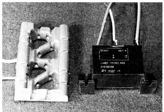
Fig. 1 Two of the several types of high-voltage rectifier in new Zenith color
TV receivers, and filter assemblies used
Automatic Tint Controls
Automatic tint control (ATC) circuits are intended to offset the undesirable and frequent changes in tint, or hue, caused by variations in the broadcast signal. Because green or purple skin colors are the most displeasing flesh tints, all of the ATC circuits increase the amount of orange in the picture.
Color-bar patterns, when the ATC is switched on, show as many as four orange bars instead of the usual one. Because some false hues will result from any ATC action that broadens the range of orange skin tones, only enough ATC should be used to keep the flesh tones relatively consistent and of an acceptable hue.
When servicing ATC-equipped receivers, remember that ATC action will change the null, or crossover, points of the color-bar signal viewed on a scope connected to the CRT, or the actual color-bar pattern viewed on the screen of the picture tube.
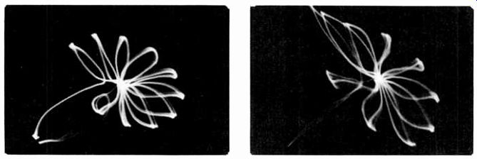
Fig. 2 Vector patterns illustrating Magnavox's ATC action. (A) Normal vector
pattern with the third petal at 90 degrees (red.) (B) The first three petals
all are at 57 degrees (orange) when the ATC switch Is in the FULL position.
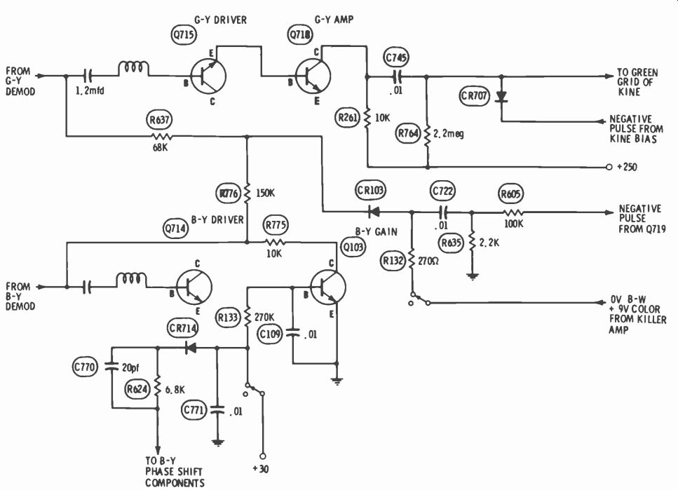
Fig. 3 The switching action of diodes and one transistor controls the ATC
circuit of the RCA CTC44 chassis.
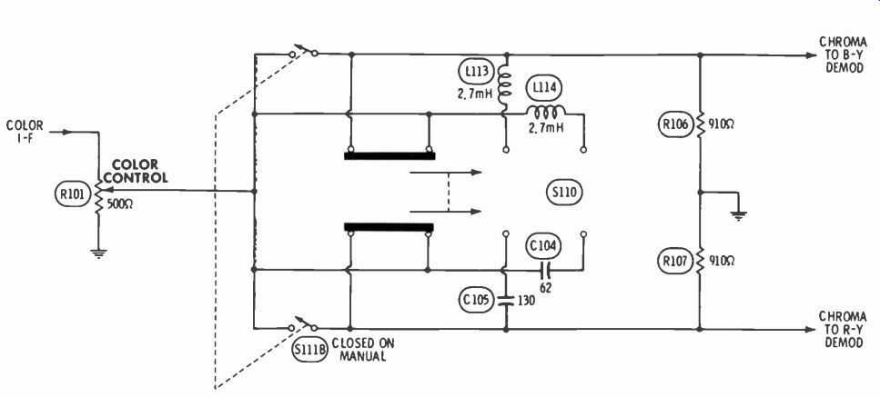
Fig. 4 Schematic of the Customatic Tint Lock circuit included in the General
Electric KE-2 chassis.
Magnavox and Admiral ATC
The ATC system in the new Magnavox T951 color TV chassis changes the phases of the yellow or red chroma signals to a 57-degree orange, which is satisfactory as skin color to most people. This is accomplished by gating on and off two transistorized channels, each of which has fixed amounts of phase shift. This correction signal then is combined with the normal chroma signal just before it is applied to the demodulators.
Vector patterns offer the fastest and most dramatic proof of this circuit action, as shown in Fig. 2.
With the ATC switch in the FULL position, the first three petals are all at 57-degrees, and even petals 4 and 10 are moved nearer to 57 degrees. Petals 6, 7 and 8 are not affected at all; these are the hues in the cyan region. (Refer to page 26 of the October '69 issue of ELECTRONIC SERVICING for a more detailed explanation of this particular ATC system.) Magnavox color TV chassis T950 employs an ATC circuit, the operation of which is based on the same principle as that used in their other models, but in which several significant changes have been incorporated.
Chroma signals from the color control are applied to the base of QA5. Output from the collector supplies the main 3.58-MHz signal to the demodulators, while the signal from the emitter goes through "Partial" and "Full" switching diodes (controlled by DC voltages) to the Red and Yellow gate transistors. It is important to notice that QA5 is the stage whose gain is eliminated by the color killer. A varicap (or varactor) diode is used in the phase-shifting network of the Preference Control. The diodes and varicap apparently are used to avoid signal radiation or degradation that could be caused by the long leads between the ATC board and the front panel, if direct switching were used.
Admiral's Color Monitor employs almost the same circuit as the one found in Magnavox color chassis T951, except a chroma driver (emitter-follower) is inserted before the "Partial" and "Full" switch and the gate transistors.
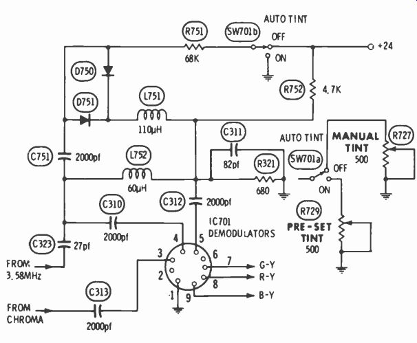
Fig. 5 The Auto Tint circuit designed into Electrohome's C9 chassis employs
diode switching.
RCA Accu-Tint
An analysis of the version of the RCA Accu-Tint (A-T) system used in the CTC39X color chassis was presented in an article which begins on page 30 of the July '70 issue of ELECTRONIC SERVICING. As explained in that article, three basic changes occur in the chroma channel when the A-T switch is turned to the ON position. These changes are: The phase of the 3.58-MHz carrier applied to the B-Y chroma demodulator is changed so that the output from this demodulator is separated from the R-Y signal by 124 degrees. Previously, beginning with their CTC16 chassis, RCA has used 105 degrees as normal phase difference between B-Y and R-Y signals.
When a color-bar pattern is viewed on the screen of the TV and the Accu-Tint is switched to the ON position, the blue bars move about a half bar to the right (away from the red bars). This multiplies the number of color bars that are orange, or nearly orange.
The output from the B-Y demodulator circuit is reduced about 33 percent.
The hue, or gray-scale, of the b-w screen is changed from the normal blue-white to a brown-white (sepia). This "warming" of the screen color "temperature" occurs only when the A-T switch is in the ON position during reception of a color signal (color killer inoperative). These same changes occur in the chroma section of the RCA all solid-state CTC44 chassis, but are the result of different ATC circuit actions. The schematic in Fig. 3 shows this part of the chroma circuit. When Accu-Tint switch SI12 is turned to the ON position, +30 volts is applied to the anode of CR714, and, because its cathode is returned to ground through R624, L710 and the secondary of the tint transformer, it is forward biased and becomes a near-short circuit.
This action connects C770 and R624 (through C771) in parallel with phase-shift components C758 and R778, which increases the phase shift of the 3.58-MHz signal that is applied to the B-Y demodulator.
The same +30 volts which is applied to the anode of CR714 also is applied, through R133, to the base of Q103. This forward–biases Q103, and the near-zero collector to-emitter resistance grounds R775, reducing the output from the B-Y demodulator.
Warming of the screen color temperature is accomplished by adding opposing pulses to the grid clamp diodes connected to the green and blue control grids of the CRT. The +9 volts that appears at the collector of 0705 the killer amplifier transistor, when a color program is received is applied through SI12 and R132 to the anode of CR 103.
This positive voltage forward biases CRI03, which passes the clamping pulse (obtained from R605, R635 and C722) on to R637 and R776. The negative pulses through R637 and R776 are amplified and inverted by the G-Y and B-Y amplifiers and finally applied to the anodes of CR707 and CR 708, which are connected to the green and blue grids of the CRT, respectively. The positive-going pulse on the green grid of the CRT and the anode of CR707 adds to the negative-going clamping pulse at the cathode of CR707 and drives the grid a few volts less positive than it would be without ATC action. Identical action takes place at CR708 and the blue grid of the CRT. Consequently, the brightness of both green and blue is reduced, while red remains the same.
GE Customatic Tint Lock
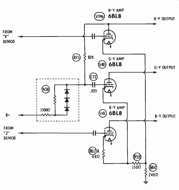
Fig. 6 A new type of matrixing is used in the production of the G-Y signal
in Philco's 21ST90 chassis.
Phases of the chroma signals applied to the B-Y and R-Y demodulators of the GE KE-2 color chassis are changed by the switch positions of the Customatic Tint Lock circuit. "Manual" and "Automatic" pushbuttons on the tilt-out control panel switch on the AFC and ATC functions in the "Automatic" position, and switch them off in the "Manual" position. Switching of the ATC action is shown in Fig. 4. In addition, S110 can be adjusted for no ATC action (110 degrees between R-Y and B-Y demodulators), moderate action (130 degrees) or maximum action (150 degrees). Because of the weaker signal and the shorter length of lead, less radiation occurs when the chroma signal, instead of the 3.58-MHz carrier, is phase shifted by ATC adjustments.
Electrohome Auto Tint
Diode switching is used in the Electrohome hybrid chassis C9 to change the phase of the 3.58-MHz carrier applied to the integrated circuit chroma demodulator, as shown in Fig. 5. The ON position of the Auto Tint switch (SW701, a front panel control) also switches in factory pre-set color and tint controls. These pre-set controls can be readjusted by a TV technician, if the customer is not pleased with the factory setting. In the OFF position of SW701, the cathodes of D750 and D751 are more negative than the anodes; consequently, both diodes are a near short, and L751 is connected in parallel with L752.
When SW701 is placed in the ON position, R751 is grounded and no DC voltage is applied to the anodes of the diodes. Because about +5 volts still is applied to the cathodes, the diodes are reverse biased, opening the circuit so that L752 is the only reactive element in the phase-shifting network. Consequently, the phase change is less than that produced with the switch in the OFF position.
Outputs from the R-Y and B-Y demodulators differ by 105 degrees in the OFF position of the Auto Tint switch and by 125 degrees in the ON position.
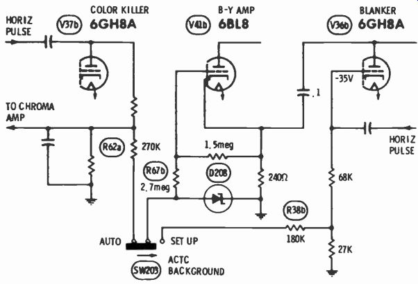
Fig. 7 Killer action in the Philco 21ST90 chassis during reception of color
signals also changes the screen color to sepia.
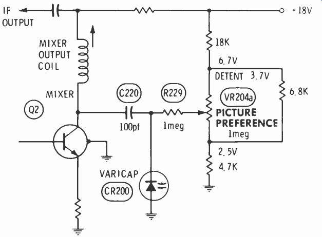
Fig. 8 A slight change of IF alignment by varicap tuning in the Philco 21ST90
chassis gives an effect similar to video peaking.
Philco Auto Tint
Philco does not have a switch or control for changing demodulator phasing, color balance or screen color of its new color receivers, but some of these features are built in.
Circuit features which produce actions that correspond roughly to a change in demodulator phasing are shown in Fig. 6. Most of the G-Y signal is developed in the common cathode circuit of the three tubes. R58 has been added to make the cyan hues less blue, and R67A slightly reduces the B-Y output.
The G-Y amplifier needs additional signal from the R-Y stage to give proper matrixing, and this is obtained easily through R71. However, a better color reproduction of degraded picture information is produced if the R-Y signal fed through R71 is more negative than positive.
The diodes and resistors in network N38 supply such a logarithmic voltage. Philco product information states that the interim quality of skin color is greenish; however when the tint control is readjusted to produce correct orange face hue, the green hues will have less blue contamination.
Philco also has an Automatic Color Temperature Control (ACTC) circuit which makes the raster color more sepia during reception of color signals. Fig. 7 shows the simplified schematic. Color-killer voltage is used to "identify" b-w or color programs for the circuit, and an ACTC set-up switch (SW203) is provided to switch in a standard voltage in place of the killer voltage, which might be undependable because of signal conditions during the adjustment.
In the SET-UP position of SW 203, a small amount of negative voltage, taken from the grid of the blinker tube, is supplied to the grid of the B-Y amplifier. To establish the desired b-w color temperature, the ACTC control is placed in the SET-UP position, and the screen color, or gray-scale, is adjusted in the usual way using the CRT drive and screen controls. Then the ACTC switch is returned to the AUTO position, in which the same amount of voltage established in the SET-UP position is supplied the grid of the B-Y amplifier by the color killer when b-w programs are received. Thus, the b-w screen color is the usual blue-white.
Because no negative voltage is generated in the color-killer circuit during reception of color signals, the grid of the B-Y amplifier is less negative than during b-w reception or when the ACTC switch is in the SET-UP position. The less negative grid causes the B-Y plate to become less positive, and because the blue grid of the CRT is coupled direct to the B-Y plate, less blue is seen in the raster and picture. Part of this same effect also is transferred to the green, because of the common cathode connections. Less blue plus slightly less green makes the raster more orange, to emphasize skin hues.
The next Philco feature to be discussed is not strictly an ATC circuit (see Fig. 8), yet it is intended to relax the rigid grip that automatic fine tuning has on the b-w picture quality. In the VHF tuner, a varicap diode is used to change the tuning of the mixer-output IF coil when the reverse voltage on the diode is changed by means of the Picture Preference Control (PPC), which is located on the front panel.
Color quality is changed very little by this feature because, as Philco states, the change in alignment is stopped before the color is degraded. A detent is provided, and the receiver has been factory aligned with the PPC control set at the de tent. Visible effect on the picture quality is somewhat the same as that produced by a video peaking control, with normal sharpness obtained at the detent. However, it is possible that better vertical and horizontal locking might be obtained on weak or poor signals with the PPC control set to smear slightly the b-w detail, compared to normal locking obtained with a video peaking control.
Zenith Auto-Tint Guard
Several of the new Zenith models use the circuit shown in Fig. 9 to improve the varying skin hues produced by some color broadcasts. Operation is straightforward: The demodulation angle between R-Y and B-Y is increased when SW204 is closed and connects C262 in' parallel with C1016.
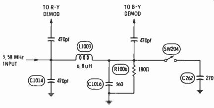
Fig. 9 The Automatic Tint Guard circuit in Zenith 40BC50 and 12B14C50 chassis
adds a capacitor to the circuitry to alter demodulator phasing.
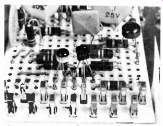
Fig. 10 Plug-in Dura-module used in Zenith's 4B25C19 chassis also features
plug-in transistors.
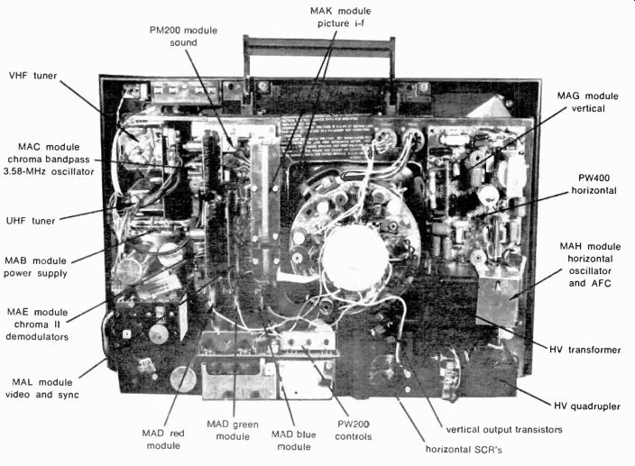
Fig. 11 Photo showing location of major components and the eleven modules
that comprise the RCA CTC49 chassis.
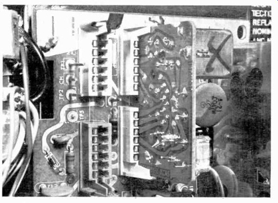
Fig. 12 Upper and lower sockets with module MAC removed from the RCA CTC49
chassis. Module PM200 and sockets are shown at right in background.
Plug-in Circuits
The expanding use of plug-in circuit boards, panels or modules could prove to be one potential source of help in relieving the added burden imposed on TV technicians by miniaturization and the added complexity of solid-state designs.
Motorola-Quasar removable panels and Zenith Duramodules (shown in Fig. 10) are well known and seem to have been well accepted.
RCA for some time has been testing the module concept in selected models of their b-w receivers. Recently, RCA announced their CT'C49 all-solid-state portable color TV chassis, which uses eleven modules. The locations of these modules and other major parts are shown in Fig. II. Fig. 12 shows the socket on board PW300 with its associated module (MAC) removed. Sound module PM22 and its socket can be seen in the background.
Pre-CRT matrixing for each color is accomplished in the three MAD modules. Fig. 13 shows both the original type, which uses conventional discrete components, and the newer version, which is an encapsulated "computer card" type that eventually will replace all the original versions of all the modules.
RCA states that the latter type gradually will be phased into production during the next few months.
Warranty on the different brands of modules varies. Motorola still has a replacement warranty on the entire panel. Zenith warrants only the individual parts on the Dura module (the transistors plug-in, as shown in Fig. 10). RCA provides a complete panel in exchange.
Motorola panels, Zenith Dura modules and the present type of RCA modules can be serviced by normal troubleshooting and repair techniques if the modules are out of warranty, or if repair seems desirable for any other reason. RCA encapsulated modules cannot be repaired with reasonable effort; therefore, replacement is necessary.
High Voltage and Automatic Brightness Control
Fewer tube-type, high-voltage rectifiers and regulators are being used because of the possibility of radiation if the high voltage becomes abnormally high.
Fail-safe circuits, tripler and quadrupler rectifier assemblies with capacitors and semi-conductor di odes in one unit, elimination of the high-voltage DC shunt regulator tube and a search for new methods of high-voltage regulation are the order of the day.
Automatic Brightness Control (ABL) circuits help high-voltage regulation indirectly by preventing excessive CRT current and, thus, any excessive decrease in high voltage (which, if severe enough, causes a noticeable amount of picture blooming). Extra Admiral Diodes Several chassis which regulate horizontal sweep and high voltage by changing the negative voltage applied to the grid of the horizontal output tube have added an extra diode in series or parallel with the one necessary for pulse rectification. The ultimate in such cautious design is the circuit in Fig. 14, an Admiral design that employs four diodes in series-parallel. Failure of any one diode (or in certain specific failures, up to three diodes) will not affect the regulation.
High-Voltage Regulation
Sweep/high-voltage regulation and ABL circuits employed in Hitachi CFA-450 and CSU-690 models are shown in Fig. 15. T703 is a saturable core reactor which changes impedance in accordance with the load on the high-voltage circuit. The Japanese-to-American translation of specifically how this circuit functions was too garbled to understand, and the actual physical construction of the reactor, which obviously is of an unusual design, was not ascertainable from the material supplied us. The Hitachi service data says that the impedance of T703 varies as the current through it changes. Thus, LX winding of T703 is in parallel with the primary of T704, the high-voltage transformer. Any reduction in the impedance of T704 because of increased load should be offset by an increase in the impedance of LX.
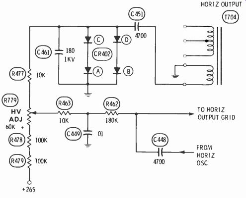
Fig. 14 To help insure adequate high-voltage regulation regardless of failure,
four diodes are wired in series-parallel in the high-voltage regulator of Admiral's
19H1O chassis.
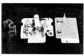
Fig. 13 Early-production MAD module and heat sink on the left, and a new type
of encapsulated MAD module on the right.
Understanding the operation of the ABL circuit is relatively easy if you imagine that R724 is connected to ground instead of +120 volts, and then realize that the voltage at the low end of the high voltage transformer secondary is the source of negative voltage which varies in direct proportion to the average amount of rectified current passing through the tripler.
(Also of help in understanding this circuit is the following rule: "When rectified DC is obtained from a diode, the polarity of the voltage will be negative if it is taken from the anode, and positive if it is taken from the cathode.") In the Hitachi ABL circuit, the negative voltage at the junction of C723 and R724 partially cancels the steady .DC voltage through R724 from the +120-volt source.
The more CRT current, the lower the positive voltage that is applied to the CRT grids. Since the cathodes of the CRT are operated at a fixed positive voltage, the CRT is biased more negatively with increased CRT current; therefore, the CRT is prevented from drawing an excessive amount of current.
Zenith Automatic Brightness Limiter
The ABL system in Zenith 40BC50 and 4B25C19 chassis does not monitor the actual high-voltage current; instead, the operation depends upon the amount of ripple in the focus voltage supply. The more high-voltage current drawn from the rectifier-filter assembly, the higher this ripple will be. Ripple (AC content) from the focus supply voltage (see Fig. 16) is coupled through C277 (inside the rectifier assembly, in some cases) and R338 to the base of Q204, which has no bias applied to it except for the ripple. If the ripple at the base is low, Q204 does not conduct and, consequently, the collector voltage, which is connected to a video amplifier stage, remains at almost the same value as the supply voltage.
When the ripple amplitude is high because of increased high-voltage current, 0204 is saturated by the large forward bias developed by the ripple, and the collector-to-emitter junction becomes a low-value resistance, which causes the collector voltage to drop, thereby increasing the negative bias on the CRT via the video amplifiers.
CRT current is limited to about 1.5 milliamperes by this ABL action.
Control of Color Saturation and Tint by Variable DC Voltages
Color and tint adjustments which are controlled indirectly by variable DC voltages instead of directly by manually adjusted controls are employed in '71 chassis of at least three manufacturers.
Such a system offers two distinct advantages: First, because the chroma IF and 3.58-MHz color sub carrier signals do not have to be routed over long wires to front panel manual controls, radiation from these signals is minimized. Secondly, remote control by variable DC voltages does not require relays and/or motors, as does remote adjustment of manual controls.
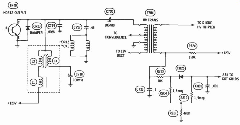
Fig. 15 Hitachi models CFA-450 and CSU-690 employ a saturable-core reactor
as the high-voltage regulator. CRT current through the high-voltage tripler
determines the amount of bias supplied the CRT by the automatic brightness
limiter (ABL) circuit.
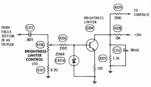
Fig. 16 The ABL circuit in Zenith's 40BC50 and 4825C19 chassis senses the
increased ripple amplitude of the focus supply voltage (resulting from excessive
brightness). The change in ripple amplitude is used to control Q204, the collector
voltage of which varies the conduction of the video amplifiers and, consequently,
also varies the bias applied to the CRT. 0204 functions as both a rectifier
and amplifier. The video amplifier voltage is directly coupled to the CRT,
in the correct polarity to reduce the brightness level.
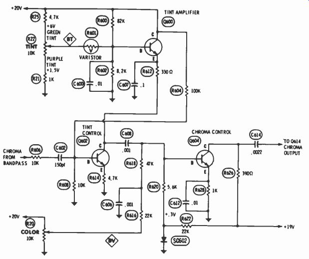
Fig. 17 Schematic diagram of the color and tint circuits in Sylvania's E01
color TV chassis. The internal capacitance of Q602 is the key to the operation
of this tint control system. Refer to the text for an explanation.
Sylvania:
One example of indirect control of color saturation and tint is found in Sylvania's all-solid-state E01 chassis. The associated circuitry is electrically located between the 2nd chroma amplifier and the chroma output stage, as shown in Fig. 17.
How the tint control circuit performs its function can be explained best by examining the results of adjusting tint control R22 to each of its extreme positions.
The actual change in the phase (tint) of the chroma signal is accomplished primarily by varying the conduction of transistor Q600. When R22 is repositioned CCW toward the position that produces greenish flesh tones, more forward bias (positive) is applied through varistor R601 to the base of Q600, increasing its conduction. The resultant increase in the emitter current of Q600 produces a larger voltage drop across emitter resistor R612, the "negative" end of which is connected to the collector of Q602. With a more positive voltage applied to its collector (relative to its base), and with a constant forward bias between its emitter and base, Q602 conducts and amplifies the chroma signal applied to its base.
Because of the inherent phase shift between the base and collector of a transistor, the amplified chroma signal at the collector of Q602 is 180 degrees out of phase with the input chroma signal at its base.
Thus, manual adjustment of the tint control to one of its extreme positions has produced a change in the DC voltages that control the conduction of the tint control transistor and, consequently, the phase of the chroma signal in relation to that of the reference subcarrier.
When tint control R22 is adjusted to the extreme CW position, which produces purple-tinted flesh tones, less forward bias is applied between the base and emitter of Q600, it conducts less, and the voltage at the "negative" end of the resistor in its emitter circuit becomes less positive. As a result of this action, the voltage applied to the collector of Q602 becomes sufficiently less positive to cut off conduction of this transistor.
Although none of the chroma signal applied to the base of Q602 is amplified when this transistor is biased off, some of the chroma signal does feed through the capacitance between the base and collector of the transistor. However, unlike the 180-degree phase shift resulting from normal transfer of an amplified signal from base to collector, the chroma signal fed through the base to-collector capacitance is not shifted in phase relative to the chroma reference subcarrier generated by the receiver.
Using this system, the phase of the chroma signal at the collector of Q602 can be varied over a range of almost 180 degrees relative to the phase of the chroma reference subcarrier, the exact phase shift depending on the vectorial addition of I) the phase of the chroma signal transferred to the collector of Q602 by transistor amplification (180 degrees shift) and 2) the phase of the chroma signal transferred to the collector via the base-to-collector capacitance (no phase shift). Color control action is by the more direct method of reducing the normal forward bias of Q604 to obtain less transistor gain. Diode SC602 provides a temperature-controlled minimum forward bias for better stability.
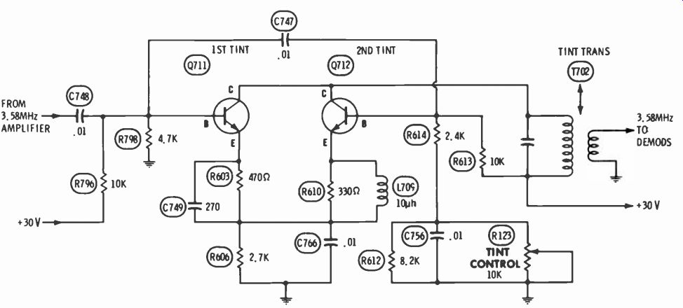
Fig. 18 The tint circuit of the RCA CTC44 chassis, shown here, is operated
by voltage and, therefore, can be used in motorless remote-control applications.
RCA
A differential amplifier is employed in the tint circuit of the new all-solid-state RCA CTC44 chassis, as shown in Fig. 18. Transistors Q711 and Q712 appear, at first glance, to be in parallel; the bases are separated by a coupling capacitor, but the signal input is of the same amplitude and phase at both bases. Both collectors are connected together. The difference between the two amplifiers is their frequency responses, which are determined by the components in their emitter circuits.
R603, in the emitter circuit of Q711, is paralleled by C749. This RC combination reduces the high frequencies from emitter to ground; consequently, amplifier 0711 increases the amplitude of high-frequency signals more than that of lower-frequency signals (opposite to the response of the degeneration or feedback). Such a stage is the equivalent of a high-pass filter, which causes a leading phase characteristic.
The frequency response of Q712 is just the opposite that of Q711; R610 in the emitter of Q712 is paralleled by an inductance instead of a capacitance. Because the emitter circuit thus attenuates the low frequencies, the amplifier produces increased gain at low frequencies. This is the equivalent of a low-pass circuit, which causes a lagging phase shift.
The combined output at the collectors will have the same phase as the input signal, if the phase shift in each amplifier is equal and opposite and both amplifiers have the same gain. The opposing phase shifts are cancelled by vectorial addition. This is the desired condition when the hue control is in the center of its range.
Any difference in the amplitude of the output signal from one amplifier compared to the output of the other causes a change in the phase of the signal at the paralleled collectors. The forward bias of Q711 is fixed, while the forward bias of Q712 can be changed by adjustment of tint control R122.
Rotation of the tint control in the direction that increases the forward bias of Q712 also increases the gain of Q712. At the same tine, the increased emitter current of Q712 raises (by way of the common cathode resistor, R606) the emitter voltage of Q711, thus decreasing the gain of Q711. At the collectors, the phase of Q712 is dominant; the output signal has a lagging phase. The exact phase is determined by the difference in the gain of the two amplifiers, at least until Q711 is biased to cutoff or Q712 reaches saturation, and this extremity is prevented by the resistor values in the base circuit of Q712.
Rotation of the tint control in the opposite direction reverses this action. The bias and gain of Q712 are reduced below that of Q711; thus, the output phase is leading.
Control of color saturation in the RCA CTC44 chassis is accomplished by a voltage-controlled variable voltage divider and by a change of bias which, in turn, changes the gain of the 3rd chroma IF amplifier transistor (see Fig. 19). The arms of the voltage divider consist of R724 (1K ohms) and diode CR709, whose internal resistance decreases as its forward bias is increased. The resistance of CR 709 varies from 6.8K ohms at about 0.68 volt, to 750 ohms at about .75 volt, and to even lower values when supplied with higher forward bias voltages. The anode of CR709 is bypassed to ground. This enables the diode to function as the shunt leg of an AC voltage divider, in addition to being the source of a DC voltage that changes the emitter voltage (forward bias) of 0704 and, thus, its gain.
Transistor Q704 is operated as a grounded base type of amplifier, in which the input signal is applied to the emitter. When the color control is turned down (rotated CCW) maximum DC voltage is applied to the anode of CR709. The DC path from the cathode to ground is completed through R724 and L708; consequently, maximum voltage is dropped across CR709, and the internal resistance is at a minimum.
This voltage divider action reduces the chroma signal (from C726/ L708) before it is supplied to the emitter of 0704. Emitter DC voltage is at maximum because of the additional voltage entering through CR709; therefore, the forward bias and the gain of 0704 are both at minimum.
Clockwise rotation of the color control reduces the DC voltage applied to the anode of CR709, increasing the resistance of the diode (shunt arm of the voltage divider) and supplying more chroma signal to the emitter of Q704. Because the increase in the resistance of CR709 allows less DC voltage to reach the emitter of Q704, the emitter voltage decreases (forward bias is increased) and the transistor produces higher gain.
To avoid bandwidth and phase changes, the load across tuned circuit C726/L708 needs to be relatively constant during color saturation adjustments. This is accomplished as a result of the fact that while the resistance of CR709 is minimum when the color control is turned down, the resistance of the path through R742 and the emitter base junction of 0704 is maximum.
These conditions are reversed when the color control is turned up; thus, a fairly constant load is applied to the tuned circuit regardless of color control variations.
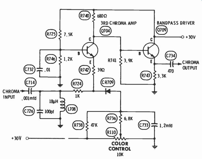
Fig. 19 The resistance of diode CR709 and the bias of Q704 are changed by
one voltage to control color saturation in RCA's CTC44 solid-state color chassis.
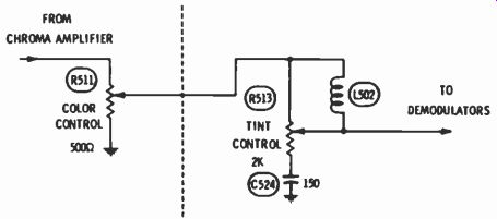
Fig. 20 Control of tint in GE's N-1 chassis is accomplished by phase shifting
the chroma signal.
Other New or Changed Chroma Circuitry General Electric-Color and Tint Control
After analysis of the preceding relatively complicated circuits, the manually-operated color and tint circuits of the General Electric N-1 portable color receiver (Fig. 20) seem even more simple than they are.
The color control action is conventional. The tint control is turned completely clockwise, L502 is shorted out and C524 has little effect because it is isolated by the 2K-ohm resistance of the control. Therefore, the phase of the chroma signal is unchanged.
Full CCW rotation of the tint control changes the circuit to a lowpass filter. The upper leg of the filter is L502 in parallel with R513, and the shunt leg is C524. This filter shifts the phase of the chroma signal by more than 100 degrees (lagging).
Sylvania-Chroma Sync Locking
A phase detector, DC amplifier and a varicap (varactor) diode are used in the Sylvania D16-2 color chassis to lock the 3.58-MHz crystal oscillator (Fig. 21). The phase detector action is conventional except for the bias voltage for Q620, which is obtained through the phase detector.
Q620 actually consists of two cascaded emitter-follower transistors ( Darlington pair) in one case. This type of operation provides very high input impedance. Error-correction voltage from the phase detector, plus forward bias, is applied to the base of Q620. Amplified error-correction voltage from the collector of Q602 is applied to the cathode of varicap diode SC608, whose anode is connected to a regulated voltage of about +7.6 volts, to establish reverse bias. The internal capacitance of SC608 changes when the voltage across it is changed. This capacitance, which is in series with the 3.58-MHz quartz crystal, changes the frequency of the color oscillator to accomplish and maintain chroma locking.
Electrohome-Pulse Clamping of CRT Grids
Pulse clamping of the DC voltages at the grids of the CRT in the Electrohome C7 chassis is provided by the circuit shown in Fig. 22. The two purposes of such a circuit are:
1) to prevent variations in the plate voltages of the-Y amplifier tubes from changing the b-w screen color; and, 2) to reset the DC voltage at each grid of the CRT during each horizontal cycle.
Both a negative-going pulse from the blanker tube and positive DC from the CRT bias control are present at the junction of R752, R755 and the cathode of D707. The CRT bias control supplies (through R755 and R752) a DC voltage of slightly more than the amount eventually needed at the grids of the CRT. Capacitor C736 accepts and stores a charge because of the difference in DC voltages between the plate of the-Y amplifier and the grid of the CRT. Because the tip of the negative-going horizontal pulse at the cathode of diode D7O7 is less positive than the voltage at the anode (stored in C736), D707 conducts for the duration of the pulse and charges C736 to a new and lower voltage.
If a series of non-symmetrical chroma pulses at the grid of the CRT shifts the operating center to make the CRT grid more positive than it was during the previous blanker pulse, the next horizontal pulse will forward bias D707, whose conduction will lower the voltage on C736.
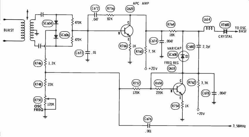
Fig. 21 Sylvania's D16-2 chassis uses a varicap diode to lock the color oscillator.
A " Darlington pair" amplifier provides DC voltage gain between the
phase detector and the varicap diode.
If the voltage at the grid of the CRT is not changed by the chroma signal, C736 is charged to a slightly higher voltage by the CRT bias voltage applied through R752. This slight increase is reduced by the next horizontal pulse.
Thus, undesirable changes in screen color are prevented by restoring the DC voltage on each grid of the CRT. As explained previously, this is accomplished during horizontal blanking, when no chroma information is present.
General Electric-Pulse Clamping of CRT Grids
A more elaborate system of pulse clamping the DC voltages at the grids of the CRT is employed in the General Electric KE-2 color chassis. Clipped and shaped sync pulses are used (Fig. 23) in place of pulses obtained from the horizontal sweep circuit.
About the same DC voltages are produced at the CRT grids when no station is received (no sync pulses) as are produced when station and sync pulses are present. Because the action is the same for all three grids of the CRT, only the effects on the blue grid will be explained here.
This pulse clamping action is easy to understand if two basic conditions are understood:
1) Transistor Q752 is an open circuit when there are no pulses present, and 2) the transistor is a near-short circuit when the sync pulse is present at the base.
When no signal is being received and, consequently, no sync pulses are present in the circuit, Q752 is open, and the grid voltage of the CRT is obtained through R762 from a +200-volt tap on the voltage divider comprised of R765, R766 and R767. With +325 volts applied to its cathode, diode CR752 is an open circuit, and the grid of the CRT floats at +200 volts because there is no chroma signal to cause it to drift. This action keeps the screen color and brightness stable.
When a signal is received, negative-going sync pulses are applied to C750, which is of sufficiently small capacitance to sharpen the pulses to a duration of 3.5 µs. The sharpened pulses then are applied to R759 and CR750, whose function is to clip the waveform so the amplitude does not exceed 0.8 volt PP. This shaped and clipped negative-going pulse at the base becomes, through normal transistor action, a larger positive-going pulse at the collector. Because the base-emitter junction of 0752 (NPN) has no forward bias, the transistor is an open circuit until the pulse from Q751 arrives through C752 and drives Q752 into complete saturation (a near-short circuit). With Q752 a near-short circuit, the resistive values of the voltage divider are changed. R756, through 0752, is in parallel with R765 and R766, and the DC voltage at point 3 increases from the "no-pulse" voltage of +167 up to +190 volts.
The same +190 volts also appears at point 1 (because Q752 is a near short circuit). Between sync pulses, CR752 is biased off by the combination of +325 volts applied to its cathode and the +200 volts at its anode.
However, during the time the sync pulse is present the voltage on the cathode of CR752 drops to + 190 volts, and the diode is biased on.
Normally, with CR752 conducting, the +200-volt charge on C740 would drop to about the + 190-volt level present at the cathode of CR 752. However, a simultaneous 25 volt increase in the voltage applied to the anode of CR752 (via R762) attempts to increase the charge on C740. The result of these two opposing forces is an increase of the CRT grid voltage to about +200.06 volts.
When the pulse is gone, the CRT grid voltage slowly decreases to the original +200-volt level. The discharge of C740 from 200.06 volts to 200 volts is slowed by the combination of R762 and the storage action of C753.
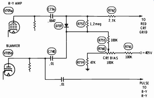
Fig. 22 Voltage clamping of the CRT grids in the Electro-home C7 chassis is
by means of "pulsed diodes."
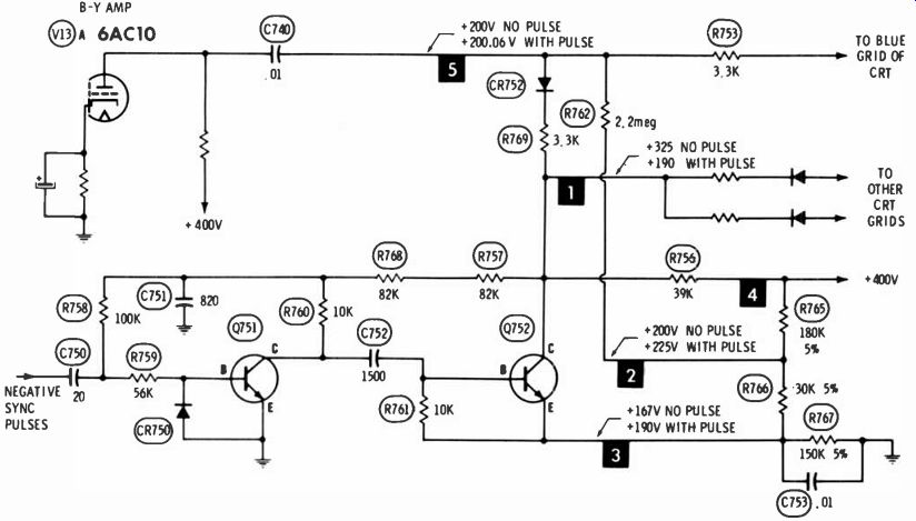
Fig. 23 The General Electric KE-2 chassis also clamps the DC voltages on the
CRT grids by diodes controlled by pulses from the sync circuit.
If a chroma signal of non-symmetrical waveshape increases the average DC at the CRT grid above +200 volts, the pulse conduction path through CR752 and R769 is dominant over the charging path through R762, so the grid is restored by the next pulse back to the normal +200.06 volts. This action prevents any build-up of higher positive voltages on the grids of the CRT. Also the capacitive coupling prevents changes in the DC voltages at the plates of the-Y amplifiers from affecting the voltages on the grids of the CRT. Such changes are undesirable, because they would change the b-w screen color.
General Electric advises that any measurement of DC voltages on the grids of the CRT be made with a VTVM having an input resistance of no less than 100 megohms, because a lower input resistance interferes with clamp action. Similarly, a scope should not be connected to a grid of the CRT; instead, connect it to the plate of the preceding-Y amplifier, where a small pulse should be found. It is advisable to observe the waveform both off channel and on a normal b-w program, to help you become familiar with the different waveforms thus obtained.
Remember, in any of these systems in which the grid circuits of the CRT are "pulsed", only a small percentage of the applied pulse ever reaches the grid of the CRT, or appears on a scope connected to the grid. The circuit action is identical to the peak-reading rectification of a pulse by a series rectifier circuit which has a large filter capacitor in parallel with the load. Only a small "ripple" remains. The capacitor connected from each-Y amplifier to the associated CRT grid performs the same function as the filter capacitor of the pulse rectifier.
A shorted clamp diode increases the DC voltage applied to its associated grid to about 275 volts, and increases the voltage to the other two grids to about 230 volts. The screen will be excessively bright over the area covered by the affected color, often to the point of blooming.
Panasonic-Auto-Color. Subcarrier Generation, and Pulse Clamping
Several new circuits found in Panasonic's CT98D color chassis are shown in the block diagram of Fig. 24.
When the Auto-Color circuit is switched on, pre-set color and tint controls are substituted for the conventional front-panel controls. In this chassis no provision is made for ATC by changing the demodulator phasing.
The "X" level control between the 2nd color amplifier and the diode-type "X" demodulator is provided to balance the red and blue chroma signals. The effect of a small amount of ATC is obtained if the "X" level control is adjusted to maximum.
"X" and "Z" transistor amplifier stages are used to increase the amplitude of these respective signals before matrixing and further amplification in the-Y amplifier tubes.
The 3.58-MHz subcarrier is generated by ringing the 3.58-MHz crystal with amplified burst. Loss of burst causes loss of the 3.58 MHz subcarrier, which, in turn, greatly weakens color "zonfetti" during b-w programs. However, because a color killer is used in this model to completely eliminate color snow when a color program is not being received, the absence of color confetti during a b-w program does not by itself indicate a loss of chroma subcarrier.
Pulse clamping of the DC voltages at the grids of the CRT by a method similar to that used by RCA and Electrohome is employed in the CT98D color chassis, with the exception that the resistor usually connected between the grid of the CRT and 3+ in RCA and Electro-home chassis is connected between the grid of the CRT and the plate of the-Y amplifier in the Panasonic chassis.
RCA-Chroma Plug-In Modules
Pre-CRT matrixing of chroma and video signals, and pulse stabilization of b-w screen color temperature are functions of the MAD plug-in modules employed in RCA's CTC49 all-solid-state color chassis (Fig. 25). The early-production MAD module, which uses conventional components and a heat sink, and the newer encapsulated "computer card" MAD modules are shown Fig. 26.
Three identical MAD modules are used, one each for red, blue and green drive to the cathodes of the CRT. As shown in Fig. 9, video is applied to the emitter circuit of Q1 through the paralleled paths of R7, R6, C2 (for increased high frequency response) and R336 to R335 (video drive control). There is no phase inversion of the video, because Q1 is a grounded-base amplifier to this signal.
The chroma-Y signal is applied to the base of Ql. Matrixing of the video and chroma signals is accomplished inside Ql. The output at the collector of Q1 is a complete red, blue or green color signal.
No signal is applied to the three grids of the CRT; only a DC voltage, which can be varied by the "kine bias" control, is present on the grids.
The collector of Q1 in each MAD module is coupled directly through a 3.3K-ohm resistor (inside the CRT socket) to the corresponding cathode of the CRT; therefore, stability of the DC voltages on the collectors of all three Q1 transistors will determine whether or not the b-w screen color remains unchanged. Stabilization of these collector voltages is accomplished by a pulse clamping circuit, which also supplies horizontal blanking.
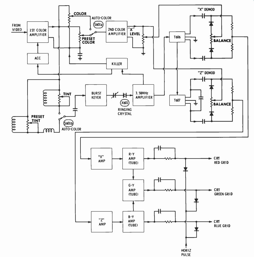
Fig. 24 A block diagram of the Panasonic CT98D chroma circuit shows pre-set
color and tint controls, "X" balance control and a variation of the
CRT grid clamp circuit.
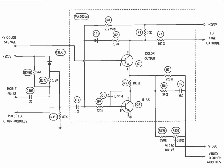
Fig. 25 Plug-in MAD module of RCA's CTC49 all-solid-state color portable receiver
incorporates pre-CRT matrixing of video and chroma signals, plus pulse stabilization
of the DC voltages applied to the CRT.
A large positive-going horizontal pulse obtained from a winding on the high-voltage transformer is applied through C3O9; R34O, R341 and R331 reduce the amplitude of the pulse and provide DC return paths. Diode CR307 "compares" the pulse to the +220-volt supply and clips off any portion of the pulse which exceeds 220 volts peak. The 220-volts (peak) pulse passes through C3 and diode CR1 (by forward biasing it into conduction), and, after attenuation to 160 volts peak by the voltage divider action of R2 and the C-E resistance of Q1, continues on to the cathode of the CRT and blanks off the associated gun. This blanking action is in addition to the horizontal blanking applied to a video amplifier.
Regulation of the DC voltage on the collector of Q1 is not quite as simple as the blanking function.
During retrace time, when no color signal is present on the collector, the DC voltage at the collector of Q1 is compared to the blanking pulse.
An error-correcting voltage developed by this comparison action is used as the variable forward bias for Q2. The variable voltage drop across the C-E junction of Q2 changes the forward bias of Q1; as a result, the DC voltage, on the collector is maintained at the desired level. These complex actions are easier to understand if the explanation is divided into three segments.
First, imagine that R8 and C3 are removed, and that R2 and diode CR1 are removed and replaced by a resistor of the correct value to provide bias for Q2. If the ambient temperature increases, Q1 draws more current, the collector voltage decreases (less positive), less forward bias through the added resistor is applied to the base of Q2, and the collector voltage of Q2 increases, as does the emitter voltage of Q1. An increase in emitter voltage represents a decrease in forward bias; consequently, the transistor draws less current and the collector voltage is increased to the same voltage that was present there before the temperature change.
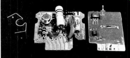
Fig. 26 An early production MAD module with heat sink is shown on the left,
and the newer encapsulated version on the right.
C1 slows the correction action to prevent overshoot or hunting.
It is obvious that a circuit which increases the forward bias of Q2 when the collector voltage of Q1 is increased also will stabilize that collector voltage at a level determined by the tolerance of the parts in the circuit. However, a standard is needed so that the collector voltage is stabilized at the desired voltage, and so that the DC voltages at the collectors of all three Q1 transistors will be nearly identical. This standard is furnished by the blanking pulse.
For the second segment, imagine that C3, diode CR1 and R2 are reinstalled according to the original wiring, but R3 is removed and the collector of Q1 is grounded. On the anode of diode CR1 will be found a non-varying negative voltage which is the result of shunt-type rectification of the horizontal blanking pulse by diode CR 1. Next, imagine that R2 is disconnected from the collector of Q2 and attached to a variable, positive DC supply. As the positive supply voltage is increased, the negative voltage at the anode of diode CR1 decreases. The reason for this action is simple, but important: Any positive voltage on the cathode of diode CR1 subtracts from the rectified (negative) voltage, because before rectification can occur more pulse is required to exceed the cathode voltage. Or to state this another way: Any positive voltage on the cathode of diode CR1 causes the same effect on the rectified voltage as would a reduction in the pulse amplitude.
The last analytical step assumes that the circuit is complete, as shown in Fig. 25. Resistor R8 supplies an unvarying positive voltage at a slightly higher level than the negative voltage from the anode of CR1, which changes when correction of the collector voltage of Q1 is required. This resultant voltage is the bias supply for Q2, and is supplied to the base of this transistor through R9. C1 filters out the horizontal pulses so that only DC voltages are applied to 02. In addition, C1 retards the speed of any correction of the voltage at the collector of Q1.
Now the stabilizing loop is complete from the collector of Q1, through the pulse circuit, bias voltage of Q2, bias voltage of Q1 and back again to the collector of Q1.
Improved Serviceability and Product Safety Motorola Quasar
The new Motorola TS934 color chassis (Fig. 27) is constructed with plug-in panels mounted in a rollout drawer, in the distinctive Quasar tradition. But in addition, the entire front panel swivels, after a few screws are removed, to permit tuner repairs or contact cleaning without removal of the tuner.
Zenith
Zenith color TV receivers which feature the 4B25C19 chassis do not require a shielded high-voltage compartment because no high-voltage rectifier, regulator or focus rectifier tubes are employed. Instead, a solid-state, high-voltage tripler, housed in a sealed assembly (behind the high voltage transformer in Fig. 28), furnishes both high voltage and focus voltage. Both the transformer and tripler arc readily accessible for testing or replacement.
Clips and brackets prevent accidental removal of the medium- and large-size transistors during transport, as shown in Fig. 29.
General Electric
Symbols of components important to the prevention of fire and X radiation are printed over a gray background on General Electric's schematics, as shown in Fig. 30. DC voltage sources and their destinations are marked with large symbols, also shown in Fig. 30. GE's use of their unique in-line guns color picture tube has been expanded to include larger screen sizes. Fig. 31 shows the relatively few convergence components necessary with this system, which permits simpler purity and convergence adjustments.
RCA
Vertical output transistors and horizontal sweep SCR's are readily accessible on the large heat sinks of the RCA CTC49 chassis (Fig. 32). High voltage and focus voltage in the new RCA chassis arc obtained from a solid-state quadrupler assembly (Fig. 33).
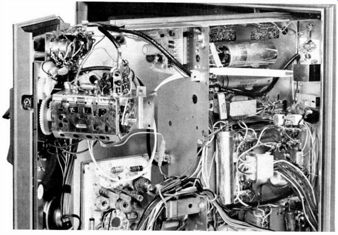
Fig. 27 The entire front panel of the Motorola TS934 swivel to permit access
to the tuners.
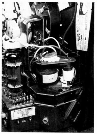
Fig. 28 No high-voltage compartment is needed in the Zenith 4B25C19 chassis;
consequently, the high-voltage transformer and the tripler assembly are easily
accessible.
Pincushion Correction
Many pincushion correction circuits have been changed. The trend is toward the use of special transformers and saturable reactors in circuits without tubes, transistors or diodes.
Packard Bell
The Packard Bell 98C32 color chassis employs the circuit shown in Fig. 34 to correct both vertical and horizontal pincushioning. The amplitude of horizontal pulses induced through pincushion modulator transformer T508 are corrected by the adjustment of R525. Resonant action of C513 and L502 shapes the horizontal pulses into near-sine waves, which are inserted in series with the vertical yoke coils.
L502 also functions as a phase, or tilt, adjustment. Simultaneously, the sawtooth waveform of vertical yoke current changes the inductance of modulator transformer T508, reducing the width of the picture at the top and bottom (the primary winding of T508 is in series with the horizontal yoke deflection coils). Zenith The pincushion correction circuit of the Zenith 4B25C19 color chassis is similar in basic concept to that of the Packard Bell circuit just described. As shown in Fig. 35, horizontal pulses from the yoke circuit are routed through the two outside leg windings of T203, thus inducing horizontal pulses into the center-leg winding. These pulses are changed into near-sine waves by the resonant circuit, comprised of L208 and C224/C246. L208 also functions as a phase, or tilt, adjustment.
The sawtooth vertical yoke current flowing through the center-leg winding of T203 also changes the inductances of the two series-connected outside-leg windings. Because the outside-leg windings are in series with the horizontal yoke coils, the horizontal sweep width is reduced at the top and bottom of the picture.
Pincushion correction for the Zenith 40BC50 and 12B 14C50 chassis is divided into separate top/ bottom and side correction circuits.
At first glance, the circuit in Fig. 36 appears to be nearly the same as that used by RCA for so many years. However, T208 is a toroidal type, whose ferrite core is doughnut shaped. The two toroidal windings in series with the vertical yoke coils are wound around the circular core in true toroidal fashion. The winding marked "outside" is wound around the entire core in the way a solenoid coil is wound. However, because the magnetic fields of the coils are at right angles, no AC signal would be induced from one type of coil into the other if two ceramic magnets were not added.
The two ceramic magnets are included with the toroidal core. Their magnetic flux is enough to nearly saturate the ferrite core. Current flowing through the outside winding also will saturate the core, and thus permit horizontal pulses to be transferred to the toroidal windings.
However, the vertical sawtooth current in the toroidal windings is not induced into the outside winding.
The horizontal pulses obtained from the toroidal windings are filtered into a near-sine wave by the resonant action of C261 and T202, which also functions as the tilt adjustment.
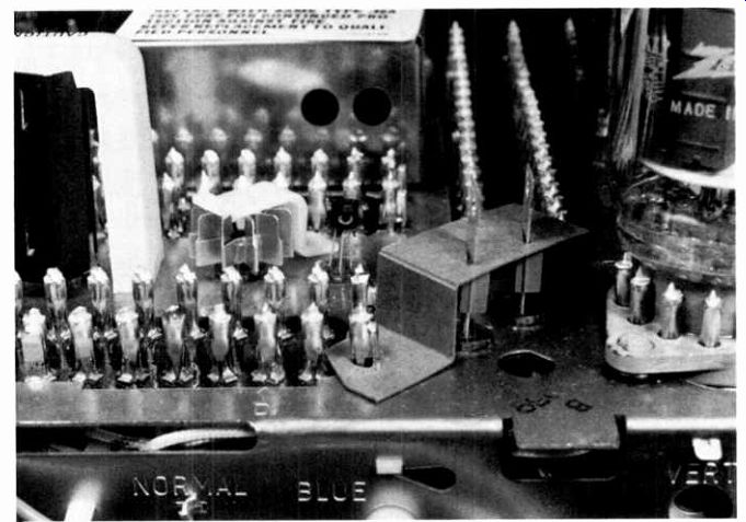
Fig. 29 Zenith provides clips and brackets to hold medium and large transistors
in their sockets during shipping.
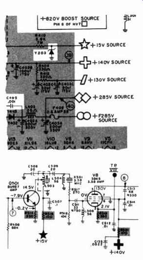
Fig. 30 Gray-shaded areas on GE schematics indicate parts that are important
to product safety or the prevention of x-radiation. Each DC voltage source
is shown by an outline of a distinctive symbol, and each connecting circuit
is indicated by a filled-in black symbol of the same shape.
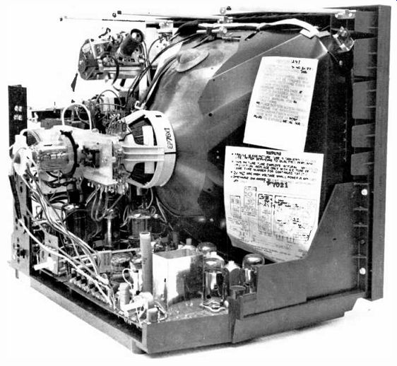
Fig. 31 There is no separate board for convergence controls in GE receivers
employing the in-line-guns CRT; all adjustments are performed by changing connector
taps and rotating magnets on the convergence assembly mounted on the neck of
the CRT.
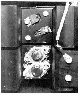
Fig. 32 The RCA CTC49 has the vertical output transistors and the horizontal
sweep SCR's mounted on conveniently located heat sinks.
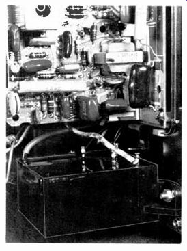
Fig. 33 Both high voltage and focus voltage in the RCA CTC49 are obtained
from the solid-state quadrupler assembly.
Side pincushion correction in the Zenith 40BC50 chassis is accomplished by the circuit shown in Fig. 37. Vertical pulses from the vertical sweep circuit are filtered into a parabolic waveform and reduced in amplitude by the actions of CR212, R313, C233, R312 (side pincushion control), R311 and C233 before they are applied to the base of transistor Q211. The amplified vertical parabolic waveform at the collector of Q211 is applied to the voltage regulator of the 128-volt supply, which furnishes the voltage for the horizontal-output stage.
Because the 128 volts applied to the horizontal output stage is reduced during the time the vertical sweep is scanning the top and bottom of the screen, the width of the raster at these points also is reduced.
Degaussing Circuits
Several of the new degaussing circuits use a bridge which becomes balanced when the positive-temperature coefficient resistor (posistor) reaches maximum resistance. This double action reduces the degaussing current to a very low value during normal receiver operation following degaussing.
JVC
The degaussing circuit of the JVC 7438 and 7408 color chassis, shown in Fig. 38, includes a double positive-temperature-coefficient thermistor, a tapped power transformer and a fixed resistor (which balances the bridge). Because both sections of R710 are cold and offer low resistance when the receiver is first turned on, almost the full 100 volts AC is applied to the degaussing coil. The resulting current through the coil heats both sections of R7I0, and the increased temperature causes the resistance of this unit to increase.
When the resistance of R710 reaches its maximum value the current through the degaussing coil will be minimum, but not quite zero. To completely stop the current through the coil, a voltage from the 110 volt tap of the power transformer is routed to the degaussing coil through R809 and thermistor R 710A, so that both ends of the degaussing coil are at 100 volts. With no voltage applied across the coil, its current stops completely, and the degaussing cycle is finished. However, current through R709 heats R710B as long as the receiver is turned on. The heat of R710B is physically transferred to R710A, to prevent R710A from cooling excessively during normal receiver operation, when no voltage is applied across R710A and the degaussing coil. When the receiver is turned off and the thermistor is allowed to cool, the degaussing cycle repeats.
Circuit actions of the degaussing circuit employed in the RCA CTC49 chassis (Fig. 39) are similar to those of the previously-described JVC design, except that a single positive-temperature-coefficient thermistor (posistor) is used.
After the thermistor is stabilized at a high resistance, voltage from the power transformer, applied through R4, lowers the voltage at the R4/ RTI end of the degaussing coil until it is equal to that at the transformer end. Sufficient current flows through R4 and RTI to keep RTI hot enough to maintain a high value of resistance.
Packard Bell
Degaussing of the CRT is not automatic in the Packard Bell 98C32 chassis, but is manually switched on by the TV viewer. This system is called "Instant Color Purity" (ICP). The advantage of this system is that the set operator can degauss the picture tube at any time while the set is operating, without waiting for thermistors to cool before the degaussing will re-cycle.
As shown in Fig. 40, the degaussing coils are in series with the AC supply to a bridge rectifier circuit which is used only for degaussing.
The ICP pushbutton switches in C509, causing a large sine wave of 120-Hz current to pass through the degaussing coil. This current rapidly decays (like a damped wave train) as electrolytic capacitor C509 accepts a charge. Because the degaussing action is so quick, it is completed before the set operator can withdraw a finger from the pushbutton. A moving, swirling color display, when the button is activated, is proof of degaussing.
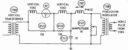
Fig. 34 The Packard Bell 98C32 color chassis uses this one circuit to correct
both vertical and horizontal pincushioning.
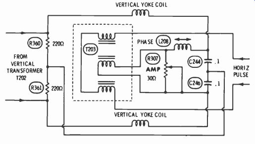
Fig. 35 Both vertical and horizontal pincushioning in the Zenith 4B25C19 chassis
are corrected by this circuit.
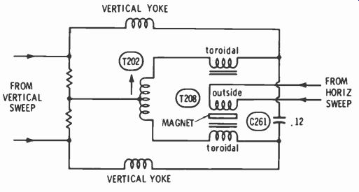
Fig. 36 New in the Zenith 408050 all-solid-state chassis is T208, which f
as a toroidal core, two ceramic magnets, two toroidal windings and one conventional
winding. This combination provides a one-way signal transference. C261 and
T202 filter the horizontal pulse into a near-sine wave for top/bottom pincushion
correction.
Chroma Circuits Motorola
An integrated circuit (IC) in the Motorola TS929 chassis is employed as three demodulators, three color pre-amplifiers and three pre-CRT matrix circuits, as shown in Fig. 41.
The outputs of the matrix circuits are not-Y signals, but, instead, are pure color signals consisting of a pre-CRT mixture of video and-Y signals which, after more amplification, are ready for direct application to the appropriate cathodes of the picture tube.
Varactor diodes (varicaps) function as variable tuning capacitors in the Motorola TT651 UHF tuner (see Fig. 42). Positive DC voltage used to control the capacitance of the varactors is selected by the channel selector switch from one of 13 potentiometers. This design enables all four of the varactors to be controlled by one voltage. The action is the same as a four-section variable capacitor which is activated by a common shaft.
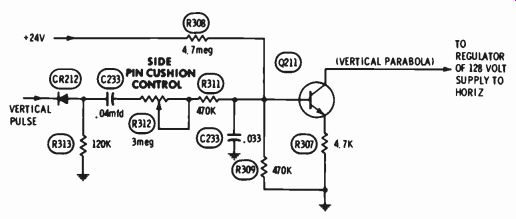
Fig. 37 Side pincushion correction in the Zenith 40BC50 chassis is accomplished
by reducing the +128 volts supplied to the horizontal output stage during the
time the sweep is at the top and bottom of the picture.
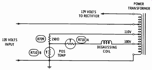
Fig. 38 The JVC 7438 and 7408 chassis employs a double thermistor plus a fixed
resistor in a bridge circuit, to more completely shut off degaussing.
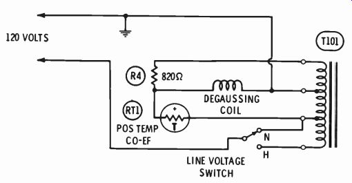
Fig. 39 A different bridge circuit is used in the degaussing circuit of the
RCA CTC49 chassis; a resistor and one posistor balance out the current flow
through the degaussing coil.
Zenith
Varactor-controlled VHF and UHF tuners plus a unique system of pre-tuning and automatic switching are combined in Zenith's new "Varactor TV Tuning System" to enable viewers to select, with a single knob and without fine tuning, any one of 14 pre-set VHF or UHF channels, or combination of VHF and UHF channels.
The new all-solid-state tuning system, a diagram of which is shown in Fig. 43, consists of: A channel-selector unit, in which all mechanical switching is accomplished; An all-electronic, FET-equipped VHF tuner whose frequency is changed by 1) changing the reverse bias applied across varicap diodes employed in its four tuned circuits and 2) triggering on and off five switching diodes which effectively insert or remove inductances from the tuned circuits so that the tuner can be tuned across both the low and high VHF bands with about the same amount of varicap control voltage.
An all-electronic UHF tuner equipped with four vari-cap-tuned circuits, one of which is a transistor RF amplifier stage (itself, a radical departure from previous UHF tuner designs). A "nerve center" unit which is constructed on a Dura-module plug-in circuit board and which, in conjunction with the channel selector unit, controls the voltages necessary for proper operation of the system.
The channel selector unit, which, as mentioned previously, performs all mechanical switching, is equipped with a drum-type, detent channel selector mechanism similar to that employed in some conventional VHF tuners. However, instead of coil strips, the Zenith channel selector mechanism is equipped with 14 vernier-type potentiometers, each of which corresponds to a desired channel.
When the channel selector is rotated to one of the 14 available positions, the full resistance of the potentiometer associated with that position is placed between a regulated +33 volts source and ground. At the same time, the slider of the potentiometer is connected to a line which is common to all varactors in either the VHF or UHF tuner. Consequently, depending upon the position of the slider, a portion of the varactor control voltage (+.5 to +28 volts) is applied as reverse bias across the varactors, changing the resonant frequency of the tuned circuits in which the varactors are used. (Changing the level of reverse bias applied across a varactor produces a corresponding change in its internal capacitance. Consequently, when the varactor is used as part of a tuned circuit, the resonant frequency of the circuit will be changed when the reverse bias applied to the varactor is changed.) A bandswitch which effectively functions as a five-section, three position switch, and which is actuated by the tuning drum mechanism after initial setup, performs the circuit changes required for switching between low-band VHF (2-6), high hand VHF (7-13) and UHF (14-83) operation, each of which relates to one of the three switch positions.
The five sections of the switch control B+, bandswitching, band-indicator lights, varactor and AFC tuning, and AGC switching, For example, in the low-band VHF position of the bandswitch:
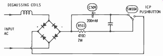
Fig. 40 "Instant Color Purity" in the Packard Bell 98C32 chassis
is initiated by a manually operated control. Current through the degaussing
coil decreases rapidly as capacitor C509 becomes charged.
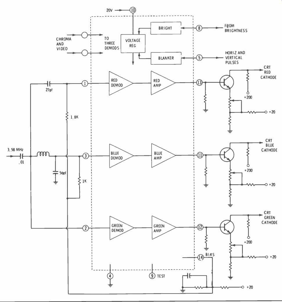
Fig. 41 The Motorola TS929 chassis employs an IC to perform demodulation,
amplification and pre-CRT matrixing.
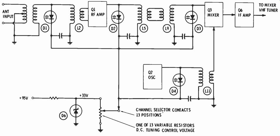
Fig. 42 Varactor diodes replace variable-tuning capacitors in the Motorola
TT651 UHF tuner.
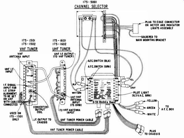
Fig. 43 Varactor-controlled tuning in both VHF and UHF tuners of the new Zenith
Varactor Tuning system makes possible one-knob tuning of 14 pre-set VHF and
UHF channels.
Section 1 switches B+ to the VHF tuner, Section 2 applies a reverse bias (negative) voltage to the five switch diodes in the VHF tuner. These diodes-X1, X2, X5, X6, and X10 in Fig. 44effectively switch more inductance into their respective circuits for low-band VHF, operation and less inductance for high-band VHF operation.
Section 3 applies filament voltage to the low-band indicator lamp.
Section 4 performs no function when the bandswitch is in the low-band position. (In the high-band and UHF positions of the bandswitch more resistance is placed in parallel with the output resistor of the AFC discriminator, to limit the variation of the AFC correction voltage and thus maintain the same frequency pull-in range as provided on the low-band position.) Section 5 provides appropriate AGC voltage to the field-effect transistor (FET) employed as the RF amplifier in the VHF tuner. A conventional (bipolar) transistor is used for the same function in the UHF tuner.
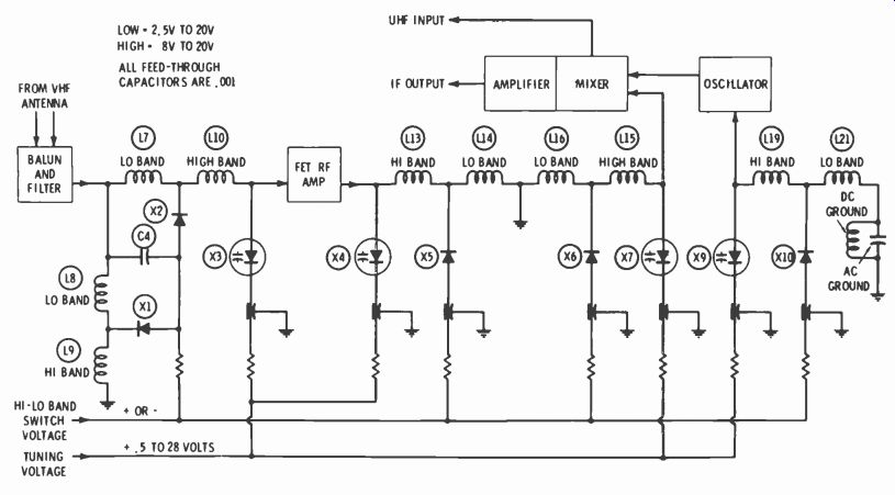
Fig. 44 A simplified schematic of the hi/lo band switching used as voltage-controlled
switches, to short out unneeded in the VHF tuner of the Zenith Varactor system.
Diodes are coils.
Consequently, because the techniques for controlling the gain of FET and bipolar transistors are different, the receiver must provide two separate AGC voltages. Thus the need for switching AGC voltages.
The design of the system also has permitted the inclusion of automatic frequency control (AFC) without the use of additional varactor diodes. AFC correction voltage is developed in the conventional manner by a discriminator circuit, except that the new AFC discriminator employed in this chassis provides a dual output, which is applied across a 6.8K-ohm resistor. When no correction is required or when the AFC circuit is manually defeated, the differential between the two outputs in zero and no voltage is dropped across the AFC resistor. When correction is needed, the two outputs become unbalanced and a level of voltage proportionate to the required correction is dropped across the AFC resistor (maximum correction voltage is ± 1 volt). AFC action is accomplished by routing the channel-selector voltage (from the slider of the potentiometers on the tuning drum in the channel-selector unit) through the AFC resistor. The voltage drop across the AFC resistor, which corresponds to the AFC correction needed, is added to or subtracted from the channel-selection voltage, which, in turn, is fed to the channel selection varactors in the tuners.
Band indicator lights and a tuning meter are provided to assist the technician in the initial setup of the tuning system. These tuning aids are controlled by the bandswitch and the nerve center circuitry.
Because the range of varactor correction voltage is almost the same for the low-and-high-band VHF functions, additional voltage must be applied across the tuning meter during high-band operation, to swing the meter needle to mid scale (channel 7 position) before channel setup of the high-band begins. This is accomplished by the tuning meter circuitry shown in Fig. During UHF and low-band VHF operation, transistor Q301 in Fig. 19 is cut off and only the varactor tuning voltage is applied across the tuning meter. When high-band operation is selected, transistor 0301 is biased on and the resultant additional current through the meter swings the needle to midscale. The needle then is positioned between the channel 7 and channel 13 positions, depending on the amount of varactor correction voltage applied to the meter.
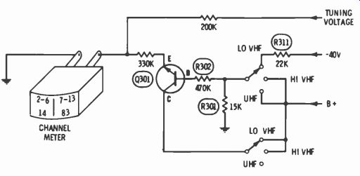
Fig. 45 A meter whose dial is calibrated to show the approximate location
of the VHF and UHF channels is used during the initial set-up of each desired
channel in the Zenith Varactor system.
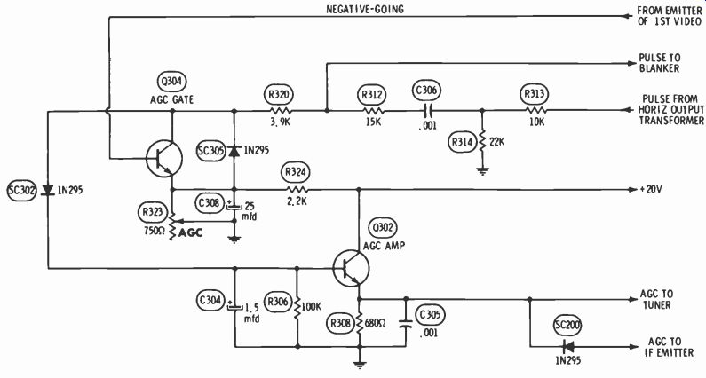
Fig. 46 The Sylvania 0-16 color chassis AGC circuit employs a transistor (0304)
as a shunt resistor to vary the amplitude of the horizontal pulse, which is
then rectified by diode SC302
Another unique feature of the tuning system involves the input circuitry to the tuners. A single antenna input balun, which can be used with either a balanced 300 ohm antenna line or an unbalanced 75-ohm coaxial line, feeds both VHF and UHF signals to the UHF tuner through a 75-ohm coaxial line. A low-pass filter in the UHF tuner then separates the VHF signal from the UHF and feeds the VHF signals to the VHF tuner through a 75-ohm cable.
A more detailed discussion of the operation and troubleshooting of Zenith's new "Varactor TV Tuning System" will appear in a near future issue of ELECTRONIC SERVICING. Miscellaneous Circuit Features Sylvania AGC Most AGC circuits, both tube and transistor, have a stage labeled "AGC gate" or "AGC keyer" which rectifies (with different efficiencies for different signal strengths) a horizontal pulse. The variable DC produced by this rectification is used as an AGC control voltage, or it varies the bias of a transistor whose output voltage supplies an AGC control voltage.
The AGC circuit of the Sylvania D-16 color chassis, shown in Fig. 46, is a departure from this traditional AGC system. Q304, although called the AGC gate, is actually the lower branch of a variable voltage divider that changes the amplitude of the pulse supplied to SC302, which performs the actual rectification. Positive DC voltage developed by the rectification is filtered by C304 and is applied to Q302 as forward bias. Because of the polarities involved, an increase in signal strength increases the forward bias on Q302, which in turn, increases (for saturation reduction of gain) the forward bias of the RF and IF amplifier transistors.
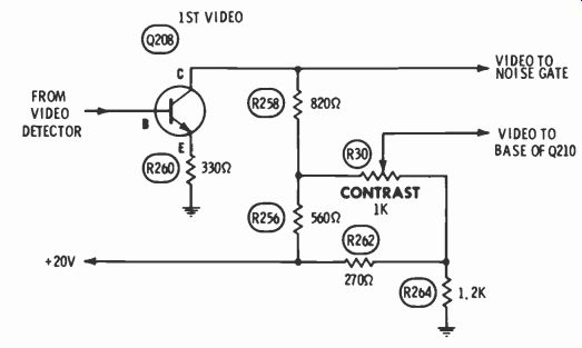
Fig. 47 DC voltages at each end of the contrast control in the Sylvania E01
chassis are nearly the same to prevent normal contrast adjustments from changing
the DC voltages in the directly coupled video stages.
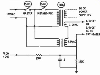
Fig. 48 Any receiver incorporating a fast-warmup picture circuit must operate
the tubes at reduced heater voltage during periods when the set is turned off.
The RCA CTC44 chassis obtains the 6 volts AC necessary for the CRT heater from
two separate power transformers. When the receiver is turned off by the "Instant
Pic" switch, 1107 continues to supply 5 volts to the heaters of the CRT.
The first action of the AGC is to lower the gain of the IF transistor, because of the voltage channeled through diode SC200. But when the voltage from the emitter of Q302 exceeds the positive bias on the IF transistor, diode SC200 is cut off. Further increases of the voltage at the emitter of Q302 arc applied only to the RF transistor.
Thus, application of AGC to the RF stage is delayed until a certain signal strength is exceeded. This prevents overload of the mixer stage in the tuner, and also establishes a good signal-to-noise ratio.
Sylvania Contrast
A different approach to contrast circuits is used in the Sylvania E01 color chassis (see Fig. 47). Part of the voltage from the collector of Q208 appears at the high side of R30, the contrast control, while the voltage divider consisting of R262 and R264 supplies a fixed DC voltage to the low end of the contrast control. Because both ends of the contrast control have approximately the same DC voltages, contrast changes, resulting from adjustment of the contrast control, have no effect on the bias of Q210, the following video amplifier transistor.
RCA Instant-Pic
The "Instant-Pic" circuit of the RCA CTC44 chassis (Fig. 48) utilizes two separate transformers to supply the heater voltage of the picture tube, the only tube used in receivers equipped with this chassis.
With master switch S103 in the ON position, T107 supplies 5 volts AC to the heater of the CRT. Although the 1-volt winding of T106 is in series with this heater supply path, the primary of T106 is not energized, so the 1-volt winding functions as a very-low-value resistor.
When the "Instant-Pic" switch is in the ON position, T106 is energized, the output of the 1-volt winding is added in series with the 5 volts from T107, and the heater of the CRT has 6 volts applied.
A DC voltage from the voltage divider consisting of two 150K-ohm resistors is supplied to minimize the possibility of heater-to-cathode shorts inside the CRT.