As we have seen from Sections 2 and 3 of this guide, much of the circuitry of a color receiver is similar to that which is found in a well designed monochrome set, a n d many of the modern circuit refinements are nothing more than the result of the normal progress of the art of electronics. The two sections of a color TV whose circuits differ from black-and-white circuitry are the chrominance channel and the picture tube itself.
In considering the chrominance circuits and the color picture tube, it is well to remember one important point: Black-and-white TV designers in the late '40's had a wealth of information from which to draw, including a great amount of practical experience obtained from WW2 electronics devices similar to television. On the other hand, many brand-new concepts were involved in the design of the first color sets. Thus, the chroma circuits are of . much more recent design and are still undergoing a certain number of "growing pains." To cite two examples, consider the continuing development of the color CRT and the numerous variations in demodulator designs in present-day sets. In this discussion of the chrominance circuits, we will consider the more popular present day designs, realizing that radically different designs are a possibility.
Block Diagram
Figs. 1 and 2 are block diagrams of two chrominance circuits.
The essential difference is whether high-level or low-level chroma demodulation is used. Low-level demodulation (Fig. 1) is an earlier design but it is by no means obsolete. At present, all the major manufacturers, with the exception of Admiral, Motorola, and Zenith, are using low-level demodulation.
As shown in Fig. 2, the Zenith design uses two tubes in the high-level demodulator while Admiral and Motorola use only a single tube.
Most of the sets that use low-level demodulation use two demodulator tubes operating on the X and Z axes. Three color-difference amplifiers are used, R Y, B Y, and G Y. The input for the GY amplifier is derived from a matrix circuit driven by the other two difference amplifiers.
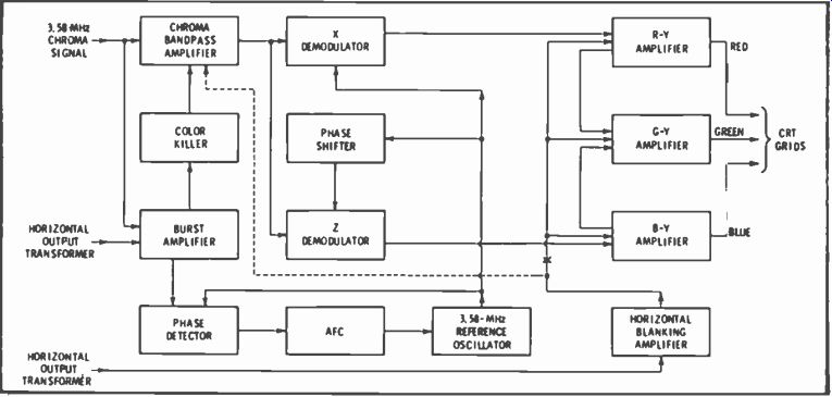
Fig. 1. Functional diagram of a chroma circuit using low-level demodulation.
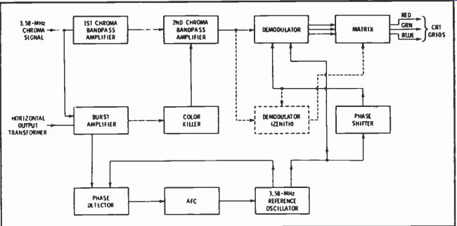
Fig. 2. Functional diagram of a chroma circuit using high-level demodulation
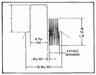
Fig. 3. Sync pulse and color burst.
General Electric has developed a demodulator circuit using diodes in a modified phase-sensitive detector. Some of their sets use three axis chroma demodulation, but others demodulate only two axes and derive a third signal, G-Y, from a matrix. In either case, RY, BY, and GY color-difference amplifiers are used. Electro-home also uses diode demodulators in some of their models.
Referring to Fig. I, there are four major functions which the chroma circuits must perform. They must reconstitute the 3.58-MHz color reference signal, amplify the chroma sidebands, demodulate these sidebands to develop the R Y, BY, and G-Y color difference signals, and amplify the difference signals to a level which is sufficient to operate the picture tube. (These last two functions are combined in circuits using high-level demodulation.) The chroma circuits perform two auxiliary functions, color killing and horizontal blanking; however, these are not essential to color operation. In fact, the color killer only operates during b-w reception, and not all chroma circuits have blanking.
The Reference Signal
From Part 1 of this guide, we recall that the 3.58-MHz chroma subcarrier was suppressed at the transmitter. There are two reasons for suppressing this subcarrier:
1. The energy contained in the subcarrier would be part of the total available transmitter power and the useful signal power would be decreased accordingly.
2. The presence of a strong 3.58 MHz signal at the video detector of the receiver would make it very difficult to prevent a 920 kHz beat from appearing in the picture. This interference could have been trapped out of sets built subsequent to the date when the color transmission standards were implemented, but b-w receivers already in service at that time would have been almost useless during color broadcasts.
Since the chroma subcarrier is suppressed at the transmitter, it must be regenerated in the receiver. This is accomplished by the 3.58-MHz reference oscillator.
This is a crystal-controlled oscillator whose phase is controlled by the color burst signal which is part of the transmitted composite video.
The color burst is a short burst of the 3.58-MHz signal generated in the color modulator. A minimum of eight cycles of this signal is transmitted immediately following each horizontal sync pulse. Fig. 3 shows the position and amplitude of the color burst relative to the horizontal sync pulse. This waveform may be observed at the output of the video detector of the receiver and this is a convenient starting point when troubleshooting a no color condition.
Referring again to Fig. 1, the composite video signal, including the color burst, is applied to the input of the burst amplifier which is biased below cutoff. A second input of the burst amplifier is an "on" gating pulse. usually taken from the horizontal output transformer. Thus. the burst amplifier is a coincidence gate which can amplify only the color burst.
After the color burst is separated from the remainder of the composite video by the burst amplifier, it is applied to the phase detector.
The function of the phase detector is similar to the familiar horizontal phase detector in that it compares a synchronizing signal with a locally generated signal and develops an error voltage proportional to the difference in phase of the two.
This error signal is used by the AFC circuit to correct the phase of the 3.58-MHz reference oscillator and synchronize it with the color burst.
The reference oscillator is a crystal-controlled oscillator which operates at the exact frequency of the reference oscillator at the transmitter. The FCC standards for the oscillator at the transmitter are 3.579545 MHz ± .0003% with a maximum rate of change of frequency not to exceed .1 Hz per second. In a well-designed receiver, the reference oscillator output approaches this same precision because it is corrected at the start of each horizontal trace--15.734 times per second.
Returning for a moment to the burst amplifier, let's consider its second function. During a color cast, a portion of the burst signal is used to cut off the color killer tube. During a black-and-white broadcast, the color killer conducts and biases the chroma bandpass amplifier below cutoff to prevent colored "snow" from .appearing on the CRT. Bandpass Amplifier The chroma bandpass amplifier is similar to a conventional IF amplifier having a center frequency of 3.58 MHz. Fig. 4A is the chroma amplifier response curve of Zenith Chassis 24MC32 which uses two stages of amplification. and Fig. 4B shows the response of the single stage amplifier of the RCA Chassis CTCI9. Notice that the Zenith response is somewhat broader. Nearly all current sets have response curves which lie within the limits set by these two curves.
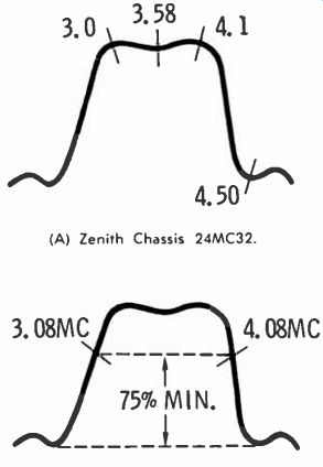
Fig. 4. Bandpass amplifier response.
The curves obtained in Figs. 4A and 4B were obtained by injecting a signal from a sweep generator at the video detector output and observing the response at the signal grid of a demodulator. An interesting variation in the method of determining the response is discussed in an article by Carl Babcoke which appeared in TEST EQUIPMENT CYCLOPEDIA, Howard W. Sams & Co.. Inc.; Cat. #50007. Using this method, known as "video sweep modulation" (VSM). a signal at the receiver intermediate frequency (45.75 Mhz) is modulated by a video-frequency sweep generator operating between approximately 2 and 5 Mhz with suitable markers injected. 1 be response curve shown in Fig. 5 is typical of the curve that should be observed at a demodulator grid. This method of observing the response of the chroma bandpass amplifier takes into account any misalignment of the video IF strip and is a valuable "quick check" for overall alignment of the receiver.
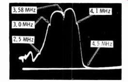
Fig. 5. Typical overall response of IF and chroma (VSM method).
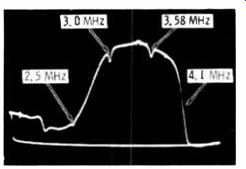
Fig. 6. Incorrect overall response curve (VSM method).
This rather lengthy discussion of the bandpass characteristics of the chroma amplifier and the reference to overall bandpass was included because of the importance of correct bandpass in obtaining a good color picture. Even the rather moderate change in response shown in Fig. 6 (same method of observation as Fig. 5) will seriously degrade the color performance of a set. Indeed, there are cases on record where a too sharply tuned antenna has made color reception impossible even though the receiver bandpass was well within tolerance.
Again referring to Figs. I and 2, the input to the chroma bandpass amplifier is the 3.58-mHz chroma information. The 4.5-MHz audio subcarrier is rejected by traps. discussed in Part 2 of this series. and the luminance or Y signal and the sync pulses are blocked by a small coupling capacitor between the video detector and the bandpass amplifier. The design of some receivers (the RCA CTC 12 chassis, for example) incorporates a circuit which cuts off the bandpass amplifier during horizontal retrace.
Generally, a single-stage bandpass amplifier is used in conjunction with low-level demodulators, and two stages of amplification precede a high-level demodulator. At any rate, the output of the hand pass amplifier, which is applied to the demodulators, is a 3.58-MHIz signal whose phase is determined by the hue of the picture being transmitted at that particular moment. The amplitude of this same 3.58-N Hz signal is determined by the intensity, or degree of saturation, of the hue.
Chroma Demodulation
In part I of this series, it was explained how the three primary colors could be modulated on a single carrier without losing any of the information. By a reversal of this modulation process. the color information may be obtained from the chroma signal. It is not necessary to demodulate on three separate phase axes since the third color-difference signal usually (G 1" ) may be derived from a suitable combination of the other two (R-Y and 13Y). The G-Y voltage is a combination of -.51 R-Y voltage and -.19 B-Y voltage.
Ec E =-.51 (E,, Er)
.19 (E., Er).
It can be proven mathematically that the chroma signal can be demodulated on nearly any pair of axes, but considerations of economy in design have resulted in the use of the X and Y axes in most sets.
However, some manufacturers (Admiral and Zenith, for example) use the R-Y and BY axes. Fig. 7 shows the more important phase angles involved in color modulators and demodulators. The 1 and Q axes are no longer being used for demodulation, by the way.
An inspection of Fig. 7 will show that the R-Y and B-Y axes are not far removed from the X and Z axes. Thus, the axes of demodulation of nearly all sets of current design are approximately the same.
Referring to Fig. 1, the chroma signal is applied to the X and Z demodulators in the same phase.
A potentiometer in the output of the bandpass amplifier is used to adjust the amount of color signal which is fed to the demodulators. This is a front-panel control and is usually labeled "Color" A second input, from the reference oscillator, is also fed to the demodulators; however, the phase of the reference signal is not the same at each demodulator. If the X and Z axes are being used, the reference signals at the two demodulators differ by 63.9°; or, in the case of R-Y and B-Y demodulators, the phase difference is 90°. In an}' event, the function of the X demodulator is to produce an output which is proportional to the chroma information present along this particular axis. By the same token, a Z demodulator produces an output corresponding to the chroma information on the Z axis, an R-Y demodulator detects the information present on its axis, etc.
We will take up the specific circuitry of the various demodulators later in the series.
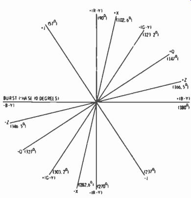
Fig. 7. Chroma demodulator axes.
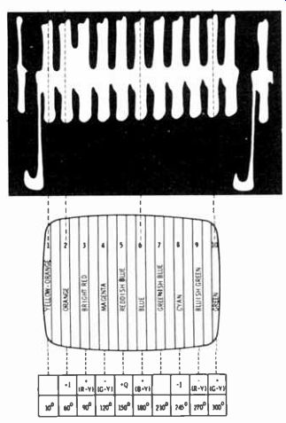
Fig. 8. Keyed-rainbow chroma signal, CRT presentation, and phases.
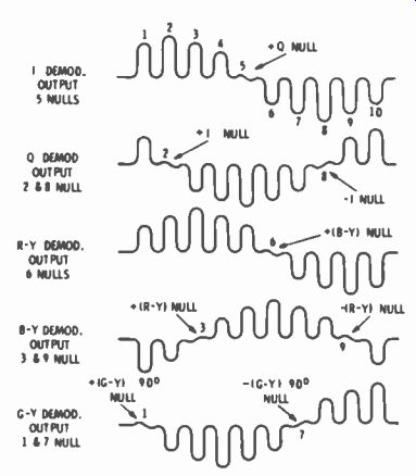
Fig. 9. Demodulator waveforms.
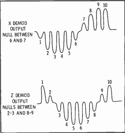
Fig. 10. Demodulator waveforms.
While many texts explain the operation of the demodulators by proving what outputs will be present for a number of hypothetical input-signal phases, it is perhaps more meaningful to show the demodulator outputs which result when a keyed-rainbow signal is fed into the set. Fig. 8 shows the waveform that will be observed at the signal grids of the demodulators.
Notice that there are eleven energy pulses, in addition to the color burst, although only ten bars are normally seen on the color receiver.
The eleventh pulse occurs during retrace and cannot be seen, and, of course, the burst pulse is invisible on the CRT. Fig. 8 also shows the color bars produced by the first ten energy pulses along with the phase angle of the chroma signal at the center of each color bar. The various axes which were shown in Fig. 7 also appear again in Fig. 8.
Fig. 9 shows the outputs of I, Q, R Y, B Y, and G-Y demodulators. Notice that the output of each demodulator reaches a positive maximum when the signal phase is the same as the axis of the particular demodulator and reaches a negative maximum 180° later. Also notice that the output of a demodulator is zero when the signal is displaced 90° from its axis.
These zero-output points, or nulls, are more frequently discussed since they are more easily observed than the maximum output points.
It is customary to observe the waveforms of the X and Z demodulators after their outputs have been amplified by the color-difference amplifiers. Under these conditions, the X and Z signals will be identical to the R Y, BY, and GY signals because the points of observation are the same; i.e., the CRT grids. If the output of the X demodulator is observed directly, the waveform is similar to an inverted R-Y output waveform; but the maximum negative output will occur at a point between the third and fourth bars, the null is between the sixth and seventh bars, and the maximum positive output is between the ninth and tenth bars.
Fig. 10 shows the output from the X and Z demodulators when a keyed-rainbow signal is fed into the receiver. Notice that the output of the Z demodulator is similar to the inverted BY waveform of Fig. 9, but that it is shifted slightly in phase (13.5°). Color Difference Amplifiers Referring again to Fig. 1, the outputs of the X and Z demodulators are fed to the R-Y and B-Y difference amplifiers, respectively.
These amplifiers and their associated circuitry amplify and invert their inputs and feed them to the CRT control grids. It is common practice to connect the cathodes of the three color difference amplifiers together and to leave the cathode resistor unbypassed. Thus, a portion of both the R-Y and B-Y signals are mixed together and fed to the cathode of the G-Y amplifier. In addition, a portion of the R-Y amplifier output is fed to the grid of the G-Y amplifier. In this manner, R-Y and B-Y are combined to form GY. Also notice that, because of the common cathode arrangement, some B-Y voltage is fed to the R-Y difference amplifier and vice-versa.
The effect of this is to cause the output of the R-Y amplifier to actually be the R-Y voltage although the apparent input to the amplifier is the X-axis voltage. A similar action takes place in the B-Y difference amplifier.
As noted previously, not all manufacturers incorporate horizontal blanking in the chroma circuit.
When horizontal blanking is used, the usual arrangement is to apply a positive pulse to the cathodes of the difference amplifiers to cut them off during horizontal retrace. In some sets, horizontal blanking is accomplished in the chroma bandpass amplifier.
A variation from the conventional low-level demodulator design was noted previously in this article.
This is the circuit used by General Electric in which three separate demodulators (R-Y, B Y, and G Y) were used. Obviously, since the G-Y axis is demodulated, it is not necessary to derive this voltage from a matrix.
Referring to Fig. 2, notice that the outputs from the demodulators are of sufficient amplitude to drive the CRT. By definition, this is high-level demodulation. Since there are no color-difference amplifiers, it is somewhat more convenient to use the R Y, B Y, and G-Y axis for demodulation. The circuitry used by the three principal proponents of high-level demodulation (Admiral, Motorola, and Zenith) will be discussed later in this guide.