POWER AMPLIFIERS are current amplifiers. The vacuum tube, transistor or other device used in a power amplifier circuit must be capable of handling much greater current than a voltage amplifier. Consequently, power tubes and transistors are generally larger physically and must dissipate more heat. Distortion is also a problem requiring special treatment, but efficiency is higher.
SINGLE-ENDED AUDIO POWER AMPLIFIERS
Figure 3.1 shows a single-ended audio power amplifier using a pentode tube. Figure 3.2 shows a similar amplifier using a transistor.
Distinguishing Features
Single-ended audio power-amplifier circuits are grounded-cathode or common-emitter circuits, to obtain maximum gain. They differ from audio voltage amplifiers in not having load resistors. Instead, an output transformer is used to transfer power from the active element to the driven device (in this case a loudspeaker), which is the real load.
Detailed Analysis
DC Subcircuit (Vacuum Tube): In Figure 3.1 electron low is from B , through R2, V, and back to B+ via the parallel paths through the primary winding of T1 and the screen-grid resistor R3. Grid bias for Class A operation (see Appendix) is established by the voltage drop across R2, and R1 serves as a grid leak. Variations in the resistance of V are caused by variations in the signal voltage applied between the grid and cathode, resulting in variations in the current lowing in R2 and the primary winding of T1. The value of R2 must be comparatively low because of the heavier current it has to pass.
DC Subcircuit (Transistor): In Figure 3.2 electron low is from B , through the primary winding of T1, Q and R3, and back to B+.
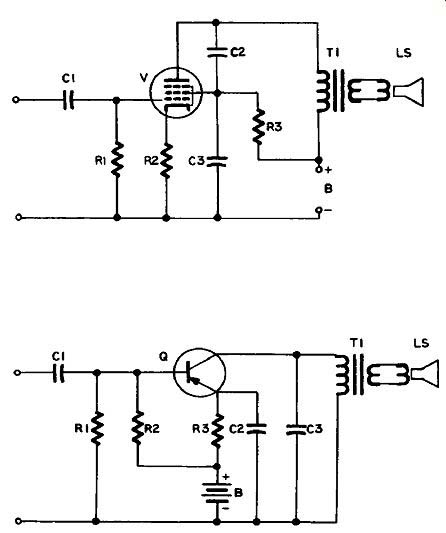
Figure 3.1 Single-Ended Audio Power Amplifier Using Pentode Figure 3.2 Single-Ended
Audio Power Amplifier Using Transistor
Bias for Class A operation is established by hole current (this is a PNP transistor), and stabilized by R2 and R3.
Variations in the resistance of Q are caused by variations in the signal voltage applied between the base and emitter, resulting in variations in the current lowing in the primary of T1. The value of R3 must be comparatively low because of the heavier current it has to pass.
AC Input Subcircuits: Both vacuum-tube and transistor amplifier inputs are RC-coupled from the previous stage in the same way as audio voltage amplifiers. In the tube circuit the cathode-bypass capacitor has been omitted to obtain degeneration, as explained in the video amplifier analysis in section 2. In the transistor circuit the bypass capacitor has been retained to keep the emitter at ground potential as far as the signal is concerned, and because degeneration would still further reduce the amplification of the transistor, which is not so great as for a pentode. Since the heavier current through R3 would still cause considerable voltage variations at low frequencies, the capacitance of C2 must be large. (An electrolytic capacitor is often used.)
AC Output Subcircuits: The output transformer used in each amplifier is an impedance-matching device. The real load is the loudspeaker.
Loudspeaker impedances are very low, from 4 to 16 ohms as a rule, whereas the plate impedance of a tube or the output resistance of a transistor is likely to be 1000 times greater. To match these different impedances (which is necessary if all the power is to be transferred) the output transformer must have many more turns on its primary winding than it has on its secondary. The turns ratio is equal to the square root of the impedance ratio. If the latter were 1000:1, then the turns ratio would have to be approximately 32:1, in theory, although it is usually made somewhat higher in practice to cut down on distortion.
The current lowing in the primary winding of the transformer consists of DC current lowing from the tube to the power source, varying in strength because of variations in the resistance of the tube. You can look at this current as consisting of two parts: a base of unvarying DC, and a superstructure of varying AC. The unvarying DC meets little resistance as it lows through the transformer winding, and because it causes no lux variations in the transformer core it has no effect on the secondary winding. The superimposed AC, however, is varying all the time, and the lux variations it induces in the core induce similar current variations in the secondary. Consequently the AC component is transferred to the secondary, but not the DC component. This AC component is the current that drives the voice coil of the loudspeaker.
In Figure 3.1, C2 is a plate-bypass capacitor and in Figure 3.2 C3 is a collector-bypass capacitor. Their value is chosen so that it will provide a path to ground for high-frequency signals which might cause high-frequency oscillation.
PUSH-PULL AUDIO POWER AMPLIFIERS
Single-ended audio power amplifiers are limited to low-power applications. Where more power is required push-pull power amplifiers are used. Figure 3.3 shows a typical push-pull audio power amplifier using tubes, and Figure 3.4 shows one using transistors.
Distinguishing Features
Two tubes or transistors sharing one output transformer, in a circuit consisting otherwise of resistors and capacitors only, indicates a push pull audio output amplifier. However, many transistor circuits now eliminate the output transformer by using low-collector-resistance transistors, but they are still easily recognizable as audio power amplifiers because of the doubling-up of transistors and because they are the final stage in the amplifier before the loudspeaker or other output.
Uses
Push-pull audio power amplifiers produce more power with less distortion than do single-ended amplifiers. This power can be further enhanced by doubling the active elements (two push-pull pairs in parallel), or by using more powerful tubes or transistors. Some power amplifiers are used to drive vibration test equipment, in which considerable loads are shaken for long periods to test the reliability of their construction. Another advantage of push-pull circuits is that they cancel out much of the harmonic distortion that is generated in pentode and beam-power tubes. Because of these factors push-pull output stages are almost invariably used in hi-fi amplifiers.
Detailed Analysis
In a push-pull circuit the input signal has to be split to feed the two output active elements. After splitting, the two signals must be of opposite phase, so that when one is swinging positive the other is swinging negative. In this way the outputs of the two tubes or transistors, applied at opposite ends of the output-transformer primary winding or other load, are of opposite polarity. (If they were of the same polarity they'd cancel each other out!) Consequently, in all push-pull circuits there must be some means of phase-splitting to obtain phase inversion for one of the output tubes. We shall discuss various methods of doing this in the following section.
DC Subcircuit (Tube): In Figure 3.3 the DC path for the two output tubes V2 and V3 is from B- to R7, which is the common cathode resistor for both. The current then divides and passes through each tube to the opposite ends of the primary winding of T1, joins again at the centertap, and returns to B+. The screen-grid supply follows the same route, except that it bypasses the output transformer. The value of the cathode resistor will be one that gives Class AB operation (see Appendix) and some degeneration to reduce distortion.
The DC path for V1 is from B- through R4, R3, V1 and R2, then back to B+.
DC Subcircuit (Transistor): The DC path in Figure 3.
4 runs from B- at the top of the diagram to B + at the bottom. There are three paths. The main path through the output transistors Q3 and Q4 also ...
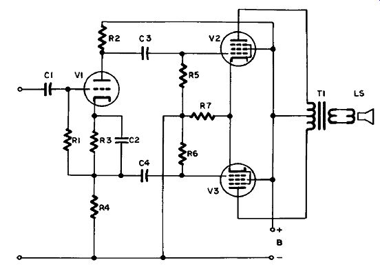
Figure 3.3 Push-Pull Audio Power Amplifier Using Pentodes, with Phase Inverter
... passes through R7 and R8. These two resistors are low value (often less than one ohm) and high wattage. They are current-limiting resistors, to protect the circuit from the effects of a sudden surge of current from B- to B+.
The second path is via Q1, R4, R5, Q2 and R6. Both these paths are designed so that in a no-signal-applied condition the voltage at the point between R4 and R5 will be half the B- voltage. (In some circuits a variable resistor is provided to adjust it, if necessary.) The third path is via R1, R2 and R3, and the base-emitter junctions of Q1 and Q2, and is for the purpose of stabilizing the bias on these transistors. The thermistor R2 is mounted on the heat sink of the output transistors so that as the temperature rises the resistance of R2 goes down (this being the virtue of thermistors). This compensates for increases in resistance with temperature in other circuit elements.
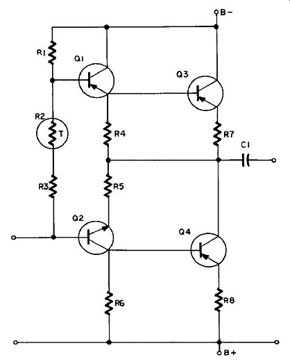
Figure 3.4 Push-Pull Audio Power Amplifier Using Transistors, with Phase Inverter.
AC Input Subcircuit (Tube): The signal is RC-coupled from the previous stage to the grid of V1. This tube is operated as an ordinary Class A audio voltage amplifier. A negative swing of the signal voltage on the grid results in a positive swing of the plate voltage, and vice versa. However , current lowing through R4, which is not bypassed, varies directly with the grid voltage. As a result, the signals coupled through C3 and C4 to the grids of V2 and V3 are of opposite phase.
Proper choice of values for R2, R3 and R4 ensures that their amplitudes are equal.
AC Output Subcircuit (Tube): With identical signals of opposite phase applied to their grids, V2 and V3 produce output signals which are not exactly symmetrical (because they are being operated as Class AB amplifiers), but which combine in the output transformer to give a true replica of the input signal. T1 couples it inductively to the load.
AC Input Subcircuit (Transistor): Q1 is a PNP transistor, and Q2 an NPN. Their characteristics are identical , and complement each other in what is called complementary symmetry. Each base-emitter junction has a small forward bias when no signal is applied, and under this condition a small current lows from B- through both transistors to B+. When a signal is applied to the input it changes the bias on each transistor, causing the currents through them to change. When the bias changes in a positive direction it opposes the forward bias on Q1, and increases it on Q2. This results in an increase in the resistance of Q1 and a decrease in that of Q2. This makes the voltage on the emitter of Q1 become less negative, so that it in turn opposes the forward bias on the emitter-base junction of Q3. At the same time the collector voltage on Q2 becomes more negative, which increases the forward bias on the emitter-base junction of Q4. When the signal voltage swings the bias in a negative direction, the opposite happens in each case.
The result is that Q3 conducts more on negative-going swings of the input signal voltage, while Q4 conducts more on positive-going swings.
Output Subcircuit (Transistor): The output circuit in Figure 3.4 is extremely simple. As Q3 and Q4 alternate between conducting more and conducting less, the voltage on the collector of Q4 swings back and forth from less negative to more negative than the resting voltage.
These are audio-frequency variations, of course, and they are coupled through C1 (an extremely high-value capacitor of probably 1000 microfarads) to a loudspeaker connected across the output terminals.
INVERSE FEEDBACK
Inverse feedback is the method used to reduce distortion in an audio power amplifier. There are two kinds. In Figure 3.5 a signal A is applied to the input of the amplifier. The output signal B is an enlarged inverted replica of A, but a spurious spike has appeared on the leading edge of the square wave. This is amplitude distortion: the amplitude of the output signal is not a faithful (enlarged) reproduction of the input signal. By feeding back to the input a portion Cx of the output signal, the distortion can be reduced. In the input the feedback signal C2 combines with the input signal A and modifies it. Being of opposite phase, it is subtracted from A to produce a new signal D. The portions enclosed by the dotted lines have been canceled out, and the modified input signal now has notches where the feedback signal had spikes. When the modified signal is amplified, the notched portions receive the same excessive amplification that gave the high spikes on B, but now the spikes are much reduced, as in E.
Amplitude distortion does not necessarily take the form of spikes. It is any deformation of the shape of the signal as it passes through the amplifier.
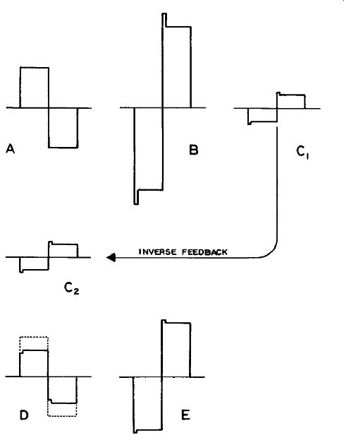
Figure 3.5 Using Inverse Feedback to Correct Amplitude Distortion
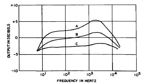
Figure 3.6 Using Inverse Feedback to Correct Frequency Distortion
The other form of distortion is illustrated in Figure 3.6. A good amplifier should amplify all frequencies equally. Curve A shows that the higher frequencies are being amplified more than the lower. By supplying inverse feedback from the output to the input in the same way as in reducing amplitude distortion, we can latten the response.
In Curve B we partially reduce the distortion by moderate feedback; in Curve C we eliminate it almost entirely by using more feedback.
You can see that inverse feedback also has the disadvantage of reducing the gain of the stage. In hi-i equipment a great deal of feed back is used to reduce distortion. Consequently the audio signal must be given increased amplification to compensate for the loss. Fortunately the distortion reduction remains at a satisfactory level.
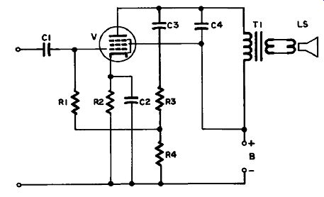
Figure 3.7 Inverse Voltage Feedback
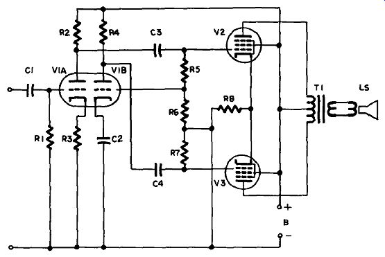
Figure 3.8
There are two types of inverse feedback. You are already familiar with inverse current feedback under the name of degeneration, obtained by omitting the cathode-bypass capacitor. It is called current feedback because the feedback signal is obtained from the current across the cathode resistor, which is varying with the signal voltage.
As you saw in section 2, inverse current feedback, or degeneration, is often used to improve frequency response.
The second method is called inverse voltage feedback, and is obtained by feeding part of the output voltage back to the input, using a circuit such as that in Figure 3.7, where the feedback is via R1 to the grid of the tube from the junction of R3 and R4. Capacitor C3 blocks the DC voltage only, so R3 and R4 are connected between the plate output and ground, or the low side of the circuit. The amplitude of the voltage appearing at their junction will depend upon their relative values. For example, if the required feedback voltage is 25 percent of the output signal, R3 will be three times the value of R4.
Inverse voltage feedback can also be supplied to the previous stage, or even to several stages. In hi-i equipment, as we've already said, a great deal of feedback is used, and it reduces the gain of each stage considerably, but as the paramount requirement is fidelity the extra expense of additional stages has to be accepted.
Circuit Variations
Another method of obtaining phase inversion for a vacuum-tube push-pull power amplifier is shown in Figure 3.8. Each half of the dual-triode tube V1 is connected as a voltage amplifier. The input signal is applied between the grid and cathode of V1 A, and the output signal is then fed to the grid of V2. This signal is reversed in phase with respect to the input signal, A portion of it is fed back to the grid of V1B, where it is amplified as the original input signal was in V1A, and the output then goes to the grid of V3. This output is also reversed in phase with respect to the input to V1B, but as the input signal to V1B was a portion of the input to V2, you can see that V3’s input will now be of opposite phase to that of V2, which is what we want.
The amplitude of the input signal to V1B must be equal to the amplitude of the input signal to V1A. This is obtained by choosing the values of R5 and R6 so that their ratio gives the required reduction.
For example, if V1A amplifies the input signal 60 times, the ratio of R5 to R6 must be 59 to 1 to get an input signal of the right amplitude to apply to V1B, so that when it has amplified it 60 times the signal fed to V3 will be the same amplitude as that supplied to V2.
Unfortunately, the two halves of the dual-triode tube may not amplify equally, especially as the tube ages. For this reason this method of obtaining phase inversion is inferior to that using a single tube.
However, since each half of the dual-triode is operating as a voltage amplifier it saves having a preceding amplifier stage. The choice there fore boils down to a matter of dollars and cents.
Phase inversion may also be obtained by using a transformer, as in Figure 3.9, where an interstage transformer T1 is shown with its secondary divided so that the upper half drives Q1 and the lower Q2. The centertap is connected via R2 to the two emitters. When one end of the secondary of T1 swings in a positive direction the other end swings in a negative direction, and vice-versa. Consequently, the signals applied to Q1 and 02 will be of opposite phase.
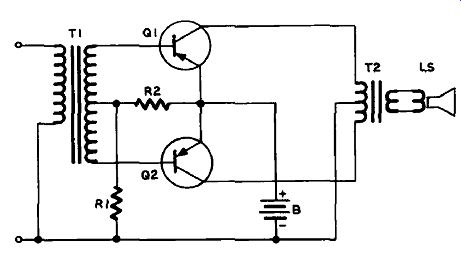
Figure 3.9 Transformer Phase Inversion
SINGLE-ENDED RADIO-FREQUENCY POWER AMPLIFIERS
Figure 3.10 shows a single-ended RF power amplifier using a triode tube.
Distinguishing Features
Single-ended RF power amplifiers are grounded-cathode circuits to obtain maximum gain. Input and output subcircuits are tuned resonant circuits: the output resonant circuit is usually a tank circuit feeding an antenna.
Tubes used in RF power amplifiers often require neutralization (see explanation in detailed analysis of the circuit). This is invariably the case with triode tubes. An RF power amplifier is operated with a much higher negative bias on the grid than other power amplifiers, requiring in most cases an external source of grid bias voltage.
Uses
Single-ended RF power amplifiers are operated as Class C amplifiers (see Appendix), and are capable of delivering moderate power (depending on the tube) to an antenna, and are used in many types of transmitters of low or moderate power.
Detailed Analysis
DC Subcircuit: In Figure 3.10 electron low is from B- through both halves of T1's secondary to the filament of V, then from the plate via the upper half of L4 and L3 to B+. Grid bias voltage is supplied by a separate source C as shown, via L2.
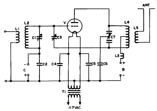
Figure 3.10 Single-Ended RF Power Amplifier
Filament Subcircuit: The plate voltage used in transmitter tubes is much higher than that used in other types, and tubes of special design are required. Dissipation of heat necessitates tubes equipped with ins or even water cooling. Oxide-coated cathodes, indirectly heated, have to be replaced with heavy tungsten filaments which can stand up to the high voltage. To heat such a filament to incandescence a filament trans former is needed to reduce the line voltage to the filament voltage used by the tube. In Figure 3.10 T1 is the filament transformer. The center tap on the secondary is connected to the low side of the circuit, to provide a path for the plate voltage, and the two ends of the secondary are connected to the filament. Both ends of the filament are also connected to the low side of the circuit through C4 and C5, which provide a path for the signal voltage but not for the filament voltage.
AC Input Subcircuit: Coil L1 is inductively coupled to L2. L2 and C1 form a series-resonant circuit, connected between the grid and filament of V via C2, C4 and C5. Maximum input signal voltage is developed when L2 and C1 are tuned to the signal frequency.
AC Output Subcircuit: C7 and L4 form a parallel-resonant circuit.
C7 is a split-stator variable capacitor. The rotor is connected to the low side of the circuit through C6, and the two stators are connected to the opposite ends of L4. The powerful current pulses from the tube become sine waves in the resonant circuit C7-L4 (as explained in section 4), and are coupled inductively to L5, and thence to the antenna. L3 is an RF choke to keep the RF signal out of the power supply.
Neutralization Subcircuit: The lower end of L4 is connected via C3 to the grid of V. Since V is a triode, energy from the plate is fed back internally to the grid, and would cause V to oscillate as it is in phase with the grid signal. However, the signal fed back via C3 is of opposite phase (being from the opposite end of L4 to the plate), and by adjusting C3 can be made exactly equal to the positive feedback, which is therefore neutralized. C3 is consequently a neutralizing capacitor.
Circuit Variations
Circuits similar to Figure 3.10 will be seen also with tubes with indirectly heated cathodes (in which no filament subcircuit is required), or using tetrodes or pentodes (in which neutralization may not always be necessary).
PUSH-PULL RF POWER AMPLIFIER
Figure 3.11 shows a push-pull RF power amplifier. As in the audio power amplifiers discussed earlier in this section, they also require some type of phase inversion.
Distinguishing Features
Push-pull RF power amplifiers are quite similar to audio push-pull power amplifiers, except for the resonant circuits used in the input and output, and provision for neutralization and an external grid-bias voltage source.
Uses
Push-pull circuits not only increase power output but also minimize distortion. This is especially true for triodes. Successive push-pull RF power amplifier stages are employed in transmitting systems between the oscillator and the antenna to develop the output power required.
They are operated as Class C amplifiers (see Appendix).
Detailed Analysis DC Subcircuit: In Figure 3.11 electron low is from B- to the cathodes of V1 and V2, thence from each plate to the opposite ends of L4, returning to B+ via the centertap and L3.
Filament Subcircuit: T1 is the filament transformer, with secondary centertap connected to the low side of the circuit.
C5 and C6 bypass the signal voltage around the transformer.
AC Input Subcircuit: Coil L1 is inductively coupled to L2.
L2 and C1 form a series-resonant circuit. C1 is a split-stator variable capacitor, with the two stators connected across the two halves of L2.
The rotor of C1 is connected via C2, C5 and C6 to the tube filaments.
When the signal induced in L2 is such that its upper end is positive, the lower end will be negative, and vice-versa. In this way signals of opposite phase are applied between each grid and filament of V1 and V2.
AC Output Subcircuit: C8 and L4 form a parallel-resonant circuit.
C8 is a split-stator variable capacitor. The rotor is connected to the low side of the circuit through C7, and the two stators are connected to the opposite ends of L4. The powerful current pulses from the tubes become sine waves in the resonant circuit C8-L4, and are coupled inductively to L5, and thence to the antenna.
L3 is an RF choke to keep the RF signal out of the power supply.
Neutralization Subcircuit: The plate of V1 is connected to the grid of V2 via C3, and the plate of V2 is connected to the grid of V1 via C4. This is called cross-neutralization. It provides signals of opposite ...
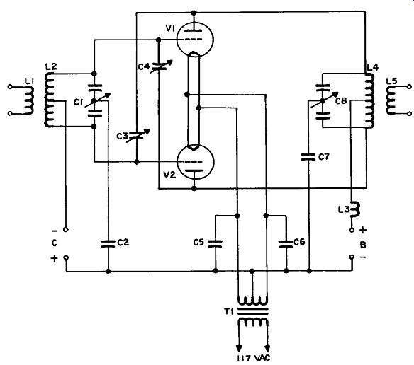
Figure 3.11 Push-Pull RF Power Amplifier
... phase on each grid to neutralize the tube's internal plate-grid feedback.
C3 and C4 can be adjusted for exact neutralization.
Circuit Variations Circuits similar to Figure 3.11 will be seen also with tubes with indirectly heated cathodes (in which no filament subcircuit is required), or using tetrodes or pentodes (in which neutralization may not always be necessary).
LINEAR RF AMPLIFIERS
Figure 3.12 shows a single-ended linear RF amplifier. In this example a pentode is used, but triodes and tetrodes may be used as in other RF power amplifiers.
Distinguishing Features
Linear RF power amplifiers are a special form of RF power amplifier, and are therefore similar in their circuitry. You can tell a linear RF power amplifier, however, by its position in the overall schematic.
Any RF power amplifier after the point where the carrier is modulated (see section 5 ) must be a linear amplifier.
Uses
As explained above, linear amplifiers, operated Class B (see Appendix), are used to bring the power of the modulated carrier up to the level required for transmission, where this has not already been done.
You can’t do this with a Class C amplifier once the carrier has been modulated, because some of the modulation will be lost.
Detailed Analysis DC Subcircuit: In Figure 3.12 electron low is from B- to the cathode of V. From V one path goes from the plate via L3 and L4 (an RF choke to keep the RF signal out of the power supply) back to B+. The other path goes from the screen grid directly to B+.
AC Input Subcircuit: This circuit is similar with that of Figure 3.10.
AC Output Subcircuit: This circuit is similar with Figure 3.10.
Neutralization: Neutralization will be required for all triodes and many pentodes. In Figure 3.12, however, we have shown a circuit without neutralization for comparison with Figure 3.10.
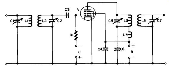
Figure 3.12 Single-Ended Linear RF Amplifier
Circuit Variations
Push-pull RF linear power amplifier circuits are similar to other RF push-pull power amplifier circuits, and are used in the same way to obtain greater power output and efficiency with less distortion than with single-ended circuits.
MAGNETIC AMPLIFIERS
In magnetic amplifiers you see a power amplifier that does not use a vacuum tube or transistor to introduce power into the circuit. In stead, a special type of transformer is used. Figure 3.13 shows a half wave magnetic amplifier, Figure 3.14 a full-wave one.
Distinguishing Features
Magnetic amplifiers consist of transformers with three or four wind ings. One (or sometimes two) of these windings is the control winding, which is supplied with direct current. This is quite a distinguishing feature, for a transformer using DC is practically never met with in any other connection. (Do not let the practice of routing the plate supply to a tube through a power output transformer, which we've just been looking at in other types of power amplifiers, confuse you, because both DC and AC are lowing in the primary of these.) A further distinguishing feature, of course, is that there are no tubes or transistors associated with the transformer in the circuit.
Uses
Magnetic amplifiers are a means whereby a large amount of power can be controlled by a quite small amount of DC. They are not used for amplifying audio or other signals, but for controlling power used in industrial applications. For example, a magnetic amplifier may be used to control the AC current supplied to a heater, maintaining a constant temperature by means of a DC current derived from a temperature sensor.
Detailed Analysis
In Figure 3.13 alternating current from a 117-volt source lows through L2 and L3 and whatever load is connected across the output terminals (AC output). If DC is required, the rectifying circuit to the right of the AC output terminals will also be required. In this case the current returns via L4 and semiconductor diode D1. D1 will only allow current to low one way, in the direction opposite to the arrow, so only the negative-going halves of the AC sine wave can pass. These are smoothed into DC by the "filter consisting of C1-L4-C2 (see section 7).
As these pulses travel through L2 and L3 they encounter inductive reactance. This reactance varies inversely with the strength of the current lowing in L1. As the DC current in L1 is increased (by adjusting R1) lux is increased in the transformer core. The core is designed to have the ability to accommodate just so much lux, so that as the DC current in L1 increases, more and more of the permeability (capability of accommodating lux) is used up, and what is left decreases. This progressively reduces the inductance of the transformer, which in turn reduces the reactance it is able to oppose to the current lowing in L2 and L3. Consequently, as we increase the DC current in L1 the AC current increases in L2 and L3. Maximum current lows when inductance is reduced to zero, at which point we say the core is saturated.
In DC applications the circuit in Figure 3.13 is less efficient than that in Figure 3.14. This is because it can only use half of the available AC, since D1 blocks all the alternate half-cycles. In Figure 3.14 this disadvantage is overcome by using both half-cycles, positive and negative, of the AC input.
This is done by means of the four-diode bridge consisting of D1, ...
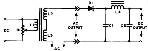
Figure 3.13 Half-Wave Magnetic Amplifier
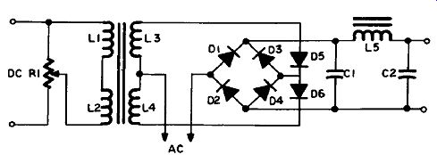
Figure 3.14 Full-Wave Magnetic Amplifier
... D2, D3 and D4. When the right-hand side of the AC input goes negative, electrons low through D2 to the low side of the output. They return via L5, D3, D5 and L3 to the left (positive) side of the AC input.
When the left-hand side of the AC input goes negative electrons flow through L4, D6 and D4 to the low side of the output. They return via L5 and D1 to the right (now positive) side of the AC input.
In this way both half-cycles of the AC sine wave are used, which is twice as efficient as in the half-wave rectifier. However, there is no loss of efficiency in the circuit of Figure 3.13 when used for an AC output, of course.
--------------------
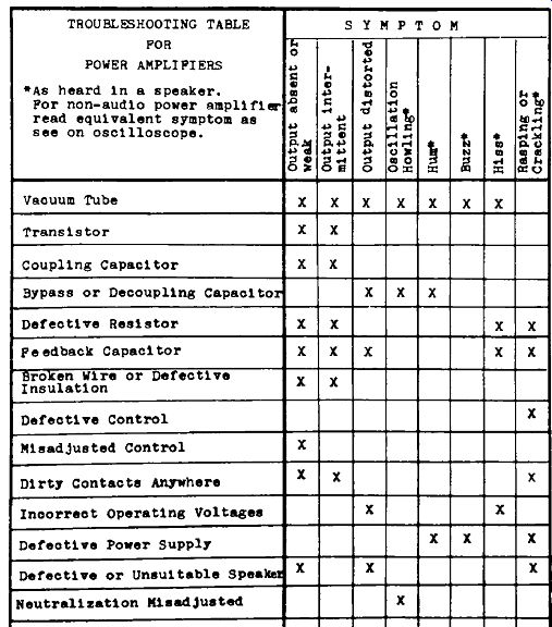
TROUBLESHOOTING TABLE FOR POWER AMPLIPIERS
As heard In a speaker.
For non-audio power amplifier read equivalent symptom as see on oscilloscope.
-------------------