A VOLTAGE AMPLIFIER is a means of using the current from a power supply or battery to produce a stronger replica of a weaker original signal. The weak signal is able to control the low of current from the power source by means of a vacuum tube or transistor. The circuit, therefore, consists of three subcircuits: one for direct current from the power source, one for the weaker input signal, and one for the more powerful output signal.
In a voltage amplifier the emphasis is on the voltage of the output signal. Since current lows at all times this type of amplifier wastes power and its efficiency is low, but its output is free of distortion be cause the excursions of the input signal remain within the distortion free limits of the tube or transistor.
AUDIO VOLTAGE AMPLIFIERS
Figure 2.1 shows an audio voltage amplifier with a vacuum tube.
Figure 2.2 shows the same circuit with a transistor. Ignore for the moment the extra resistor R1 in Figure 2.2. You’ll see the reason for it later.
Distinguishing Features
These circuits clearly it the description of an amplifier given above.
In Figure 2.1 you see a circuit in which a weaker signal input is applied between the grid and cathode of a tube in order to control the low of current from the battery so as to produce a stronger signal in the output circuit connected between the plate and cathode. Because the cathode is common to both input and output this is a common cathode amplifier-more often called a grounded-cathode amplifier.
Similarly, in Figure 2.2 the emitter of the transistor is common to both input and output, so this is a common-emitter amplifier.
Tubes and transistors can be connected with either of their other two elements common (or grounded), but the grounded-cathode and common-emitter circuits are the most used because they give the highest gain.
Amplifiers must be voltage amplifiers or current amplifiers. The latter, which are more often called power amplifiers, must be able to pass a fairly heavy current. The presence of load resistors (R2 in Figure 2.1, R3 in Figure 2.2), which always have a resistance of several kilohms, will not allow a large current output, thus eliminating the possibility that these are power amplifiers. They are, there fore, voltage amplifiers.
The absence of any inductors in these circuits shows you that they are handling audio frequencies. AF circuits sometimes have iron-core transformers or chokes, but designers today generally avoid them
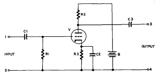
Figure 2.1 Audio Voltage Amplifier with Vacuum Tube
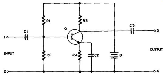
Figure 2.2 Audio Voltage Amplifier with Transistor
... wherever possible, to lower costs and to obtain a more even response to audio frequencies. Since iron-core inductors are the only type of inductor used at audio frequencies, the presence of any other type would indicate the circuit is used for higher frequencies.
Uses
Audio voltage amplifiers are used in radio and television, hi-fi, tape recorders, phonographs, public address systems and the like, to build up weak signals to the point where they can be used to control power amplifiers. For this reason you wouldn't expect to find an audio voltage amplifier in the final stage of a radio or stereo amplifier, but in the preceding stage or stages handling audio frequencies. Thus the position of the amplifier in the overall schematic is an additional way in which you can tell what type it is.
Detailed Analysis
DC Subcircuit: In Figure 2.3 electron low is from B- through R3, V and R2, and back to B+. Although the power source is shown as a battery it is in practice more likely to be one of the electronic power supplies discussed in section 7, as tube power requirements are greater than those of transistors. You’ll notice that this diagram does not show the tube’s filament circuit. It is standard procedure to show this in the power supply circuit, as in the examples given in section 7.
As far as DC is concerned R1 serves only to tie the grid to B- (zero potential), and to serve as a leakage path for any electrons gathering on the grid. The current through the resistor is negligible, therefore no voltage drop takes place across it.
In the main current path through R3 and R2 you can visualize V as a variable resistor, its resistance varying with the signal voltage on the grid. When no signal is applied to the grid a steady current will low. The values of R3 and R2 are chosen to give the proper operating voltages at the cathode and plate. A positive voltage on the cathode is provided by the voltage drop across R3, making the cathode positive with respect to the grid, which is the same as saying that the grid is negative with respect to the cathode. The value of R3 is chosen so that the voltage across it biases the grid for operation approximately in the center of the linear portion of the tube's characteristic curve (Class A operation: see Appendix).
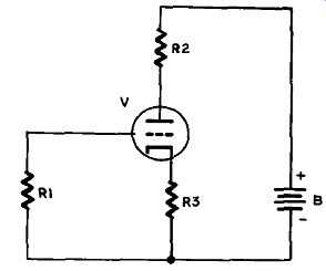
Figure 2.3 Vacuum-Tube DC Circuit
The value of R2 depends upon the resistance of V (its plate resistance). When the resistance of V varies, the current lowing through it varies, and consequently the voltage flowing through R2. The value of R2 must be such that maximum voltage variations can be obtained across it, but if it is made too large there will be too great a voltage drop for proper operation of the tube. For a triode the maximum value of R2 should not exceed three times the plate resistance. (See further on for notes on the use of pentode tubes as voltage amplifiers.) Similarly in Figure 2.4 electron low is from B- through R4, Q and R3, and back to B+. However, the bias on the base is established by the voltage drop across the emitter-base junction in the transistor instead of by the voltage drop across R4, as was the case in the tube circuit. In the tube a steady plate current lows when there is no signal on the grid. In the transistor a steady emitter-base current lows under the same conditions, which in turn permits a steady (but larger) current to low from emitter to collector. In the NPN transistor shown this will be electron current; in a PNP transistor it would be hole current. (See more about transistors in the Appendix.)
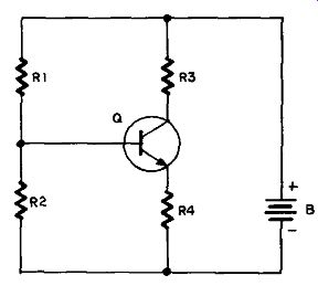
Figure 2.4 Transistor DC Circuit
The purpose of R4 is to stabilize the emitter-base current. Transistors are sensitive to temperature variations. If the temperature rises the emitter-base resistance decreases, so that the current increases.
This, in turn, allows the emitter-collector current to increase. As the current increases it heats the junctions further, so their resistance de creases further, and this situation eventually results in the destruction of the transistor if steps are not taken to prevent it.
The voltage drop across the emitter-base junction will be about .2 volt for a germanium transistor, and about .7 volt for a silicon transistor. If the current lowing through R4 results in a voltage drop of 1 volt across it, the emitter will be at a potential of +1 volt. In a germanium transistor, therefore, the base voltage will be +1.2 volts. This gives the correct forward bias across the junction for Class A operation (see Appendix).
If the emitter-base current increases due to increased temperature the current through R4 increases, with a consequent rise in voltage on the emitter. But the voltage on the base is still held at +1.2 volts by the voltage divider formed by R1 and R2. These resistors, values are chosen so that the resistance of R1 will be nine times the resistance of R2. If the battery voltage is 12 volts, nine-tenths of it will be dropped across R1 and one-tenth across R2. One-tenth of 12 is 1.2, of course, so the voltage at the junction of R1 and R2 must be +1.2 volts. Since this voltage is also the base voltage, and remains at this figure while the emitter voltage rises (or tends to), you can see that the forward bias across the junction actually decreases. This decreases the current across the junction, and counteracts the effect of the temperature rise.
As in the case of the tube, the transistor can be visualized as a vari able resistor in series with R4 and R3, its resistance varying with the signal voltage on the base. When no signal is applied a steady current will low. However, when the resistance of Q varies, the current lowing through it varies, and consequently the current lowing through R3. The value of R3 must be such that maximum voltage variations can be obtained across it, but at the same time it must also provide for the proper operating voltage for the collector of the transistor, and, as in the case of the tube circuit, the actual value has to be a compromise between these two requirements.
This circuit uses an NPN transistor. A PNP would work just as well with the battery polarity reversed.
AC Input Subcircuit (Tube): Figure 2.5 shows the AC input sub circuit for the tube. As C1 and R1 are the means of coupling it to the previous stage, it is RC-coupled. C1 also prevents DC from reaching the grid of V from the previous stage. The values of C1 and R1 are chosen so that C1 presents a low reactance to signals in the audio range, and R1 has as high a value as possible without preventing it from acting as a leakage path for electrons collected by the grid of the tube.
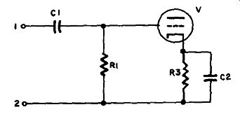
Figure 2.5 Vacuum-Tube Input Circuit
Current cannot low between the grid and the cathode of the tube, so the signal voltage divides between the low reactance of C1 and the high resistance of R1. Nearly all of it appears across R1, and consequently as large a portion of the available signal as possible is applied between the grid and cathode of V.
The value of C2 is such that it offers very low reactance to audio frequencies. Its purpose is to bypass the signal frequencies around R3, so it is called a bypass capacitor. In this way the cathode is at signal ground for AC, at the same time as it is above ground for DC.
Output AC Subcircuit (Tube):
Figure 2.6 shows the output AC subcircuit. The signal voltage on the grid is alternating between positive and negative at various audio frequencies. The grid is biased to be at a negative voltage which places the tube’s operating point in the middle of the linear portion of its characteristic curve. When the signal swings in a positive direction this negative bias is reduced, so the tube resistance is decreased and it conducts more current.
When the signal swings in a negative direction this negative bias is increased, so the tube resistance is increased and it conducts less current.
When the tube conducts more, more current lows through R2, and therefore a greater voltage is dropped across it. This makes the plate voltage less. When the tube conducts less, less current lows through R2, so the plate voltage rises. In short, a positive swing of the grid voltage results in a negative swing of the plate voltage, and vice versa.
The gain of an audio voltage amplifier such as this should be close to 100, which means that the amplitude of the voltage variations at the plate is 100 times that on the grid. Remember that although they are a faithful replica, they are 180° out of phase with the grid signal voltages.
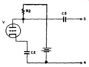
Figure 2.6 Vacuum-Tube Output Circuit
C3 can pass AC but not DC, therefore it passes the variations of voltage on the plate of the tube, because they are varying at audio frequencies, but it blocks the DC portion which is not varying. Since
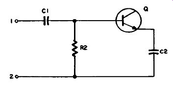
Figure 2.7 Transistor Input Circuit
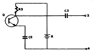
Figure 2.8 Transistor Output Circuit
C3 is coupling the output signal into the next stage the same considerations affect the choice of its value as applied to C1.
AC Input Subcircuit (Transistor): Figure 2.7 shows the AC input subcircuit for the transistor. The remarks above concerning the tube input circuit apply equally here. However, in a transistor circuit you will find that C1 has a higher value, while R2 has a lower value.
(Sometimes it is omitted altogether.) This is because the resistance between the emitter and the base is low enough to allow an appreciable current to low, so that the transistor has a low input impedance.
To avoid dropping an excessive amount of the signal voltage across C1 its value has to be such that it offers much less reactance to the signal frequency than was the case with the tube, where the grid resistor had a very high value.
Output AC Subcircuit (Transistor): In the same manner as in the tube circuit, the signal voltage on the base of the transistor in Figure 2.8 is alternating between positive and negative, resulting in variations in the voltage on the collector which reflect those on the base but are 180° out of phase with them. R3 is the load resistor across which the output signal voltage is developed.
The gain of an audio voltage amplifier such as this should be between 50 and 100.
Circuit Variations
Although the audio voltage amplifiers just discussed are typical, you are bound to meet variations in them, though not such as to make identification difficult. For example, a pentode tube could be used in place of the triode, as in the example in Figure 2.12; or the amplifier may be DC-coupled instead of RC-coupled, as in the example in Figure 2.25.
Hi-fi amplifiers usually require additional low-frequency compensation. A low-frequency limit of 100 hertz is adequate for AM radio, but a good hi-fi amplifier is expected to handle frequencies down to 20 hertz or lower, which introduces problems with the cathode-bypass capacitor.
In micro-electronics incredibly small circuits are "etched" on substrates of silicon or sapphire. On postage-stamp size "chips" hundreds of amplifiers may be formed, each having a complete circuit similar to that in Figure 2.9, which shows a typical MOS/FET amplifier. The operation of this circuit is identical to that of the triode tube already discussed. (See the Appendix for a brief explanation of the operation of a MOS-FET.) Tone controls are often found in audio voltage amplifier circuits.
The reactance of a capacitor varies with its capacitance and with the frequency of the AC passing through it. This makes it possible to de sign circuits which can attenuate some frequencies without attenuating others.
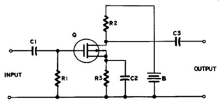
Figure 2.9 Audio Voltage Amplifier with MOS-FET
Figure 2.10 Bass Tone Control Bass Tone Control: In Figure 2.10 the input
to an audio voltage amplifier is shown with the addition of a variable resistor
R1 and capacitor C2. If the slider of the variable resistor is at the upper
end of R1 all the signal voltage applied across R2 will be shunted by C2.
The value of C2 is chosen so that it offers little reactance to higher frequencies. Consequently the higher frequencies pass readily through C2, and their voltage across R2 is greatly reduced. The lower frequencies, meeting more reactance, are attenuated less, and the lowest not at all. As a result, the bass or low-frequency end of the audio voltage spectrum becomes predominant. As the slider of the variable resistor is moved downwards, resistance in series with C2 increases, reducing the shunting effect across R2, so that the higher frequencies are attenuated less.
Figure 2.11 Treble Tone Control
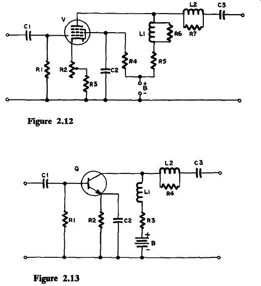
Figure 2.12 Video Amplifier with Vacuum Tube; Figure 2.13 Video Amplifier with
Transistor
Treble Tone Control: In Figure 2.11 capacitors C2 and C3 have been added between C1 and R2, and a variable resistor R1 connected in parallel with them. The reactance of C2 is very great to lower frequencies, but becomes increasingly less to higher frequencies. When R1>s slider is all the way to the right C3 is shorted out, but C2 is shunted by R1, and offers high reactance to all lower frequencies.
However, if the slider is moved all the way to the left, C2 is shunted and all frequencies bypass it, and pass through C3 (which has a much higher value) without attenuation. Intermediate positions of the slider give proportionate attenuation to lower frequencies.
We have analyzed this audio voltage amplifier circuit in greater detail than we shall analyze most of the other circuits in this guide.
This is such a basic circuit that most of its features will be found over and over again in other circuits, so that it will not be necessary to re peat the explanations given here. Instead, we shall continually refer to this section.
VIDEO AMPLIFIER
Video amplifiers are similar to audio voltage amplifiers except for additional features required to broaden the frequency response.
Figure 2.12 shows a typical video amplifier using a vacuum tube. Figure 2.13 shows another with a transistor.
Distinguishing Features
Video amplifier circuits are grounded-cathode or common-emitter circuits (to obtain maximum gain), and have load resistors (to obtain a voltage output) in the same way as audio voltage amplifiers.
However, they are different from circuits handling only audio frequencies since they require peaking coils to extend their high frequency response. L1 and L2 are peaking coils, which with their associated resistors are characteristic identifiers for video amplifier circuits.
Uses
Video amplifiers are voltage amplifiers which have to amplify the demodulated television signal so it can drive the picture tube. They are, therefore, found in television sets between the picture tube and the video detector. Whereas the maximum frequency handled by audio voltage amplifiers does not usually exceed 30 kilohertz, the video frequency range extends to 4 megahertz.
Detailed Analysis
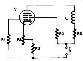
Figure 2.14 Vacuum-Tube DC Circuit
DC Subcircuits: In Figure 2.14 the electron f low is from B through R3, R2, V and back to B+ through the parallel paths of R4 and L1-R5. The main difference between this DC circuit and the triode circuit is the additional path through R4, which drops the sup ply voltage to the proper value for the screen grid of the pentode.
You can visualize V as a variable resistor, its resistance varying with the signal voltage on the control grid. The resultant changes in current lowing through load resistor R5 provide the required voltage output.
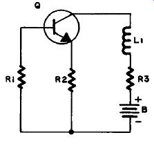
Figure 2.15 Transistor DC Circuit
A positive voltage on the tube cathode is obtained by the voltage drop across R2 and R3. In the absence of a signal the steady tube plate current will give a voltage that will bias the grid for Class A operation (see Appendix).
The grid-leak resistor R1 keeps the grid at zero potential (or negative with respect to the positive potential on the cathode).
The value of load resistor R5 is considerably lower in a video amplifier than in an audio amplifier, though still several kilohms, to avoid high-frequency attenuation. The peaking coil L1 offers no impedance to DC.
Similarly, in Figure 2.15 electron low is from B- through R2, Q, L1 and R3, and back to B+. Bias on the base is again established by the voltage drop across the emitter-base junction in the transistor.
With no signal on the base, steady emitter-base current lows, which in turn permits a steady (but larger) current to low from emitter to collector. In the NPN transistor shown this will be electron current; in a PNP it would be hole current (see Appendix).
The purpose of R2 is to stabilize the emitter-base current.
Visualize the transistor as a variable resistor in series with R2 and R3, its resistance varying with the signal voltage on the base. When the resistance of Q varies, the current varies, including the current through R3. The value of R3 must be such that maximum voltage variations can be obtained across it , but at the same time it must provide for the proper operating voltage for the collector of the transistor, and not permit undue degeneration of high frequencies in the output circuit.
This circuit uses an NPN transistor. However, a PNP would perform just as well if the battery polarity were reversed.
AC Input Subcircuit (Tube): Figure 2.16 shows the AC input subcircuit for the tube, which is RC-coupled (see Figure 2.5).
In this circuit there is no cathode-bypass capacitor as there was in Figure 2.1. The reason for this is that at low frequencies its reactance may be as high as or higher than the cathode resistor. Therefore these low frequencies would suffer degeneration.
Degeneration is caused by the voltage on the cathode varying in accordance with variations in the signal voltage on the control grid.
When the grid voltage swings in a positive direction the current flowing through R2 and R3 increases, so that the voltage on the cathode increases. This results in a smaller potential difference between the grid and cathode than would have been the case if a cathode-bypass capacitor had been present to ground the cathode voltage variations.
When the grid voltage swings in a negative direction the current through R3 and R2 decreases, so that the voltage on the cathode de creases, again canceling out part of the potential difference between grid and cathode. Actually, the total resistance of the tube is increased, so you get a smaller output signal, but as the degeneration is the same for all frequencies the lower frequencies are not penalized.
The variable resistor R2 is a contrast control. It operates by varying the potential difference between the grid and cathode, thereby effectively varying the tube resistance, and ultimately the strength of the picture on the TV screen.
Degeneration has the overall result of decreasing the amplification of the circuit. For this reason a higher gain tube is required than would be the case without it. Pentodes with high gain are used in preference ...
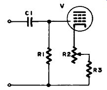
Figure 2.16 Vacuum-Tube Input Circuit
... to triodes, and sometimes more than one stage is required. The output signal is reversed 180° with respect to the input signal.
Output AC Subcircuit (Tube): Figure 2.17 shows the output AC subcircuit for the tube. C3 couples the output signal into the next stage, and the same considerations affect its choice as apply to C1.
Capacitor C2 bypasses the screen-grid resistor so that the screen grid remains at AC-ground potential for signal frequencies, to prevent de generation. Any circuit which bypasses unwanted AC to ground is called a decoupling circuit.
The main concern in the output circuit is to prevent attenuation of the high-frequency end of the video spectrum. The reason for this attenuation is that a certain amount of capacitance exists between the high and low sides of the circuit anyway, and the higher frequencies " leak" to ground through it. This capacitance is not due to actual capacitors, but to the natural capacitance that exists between various components and wires, and is called distributed capacitance. At higher frequencies the effect of distributed capacitance becomes so great that such signals bypass the load resistor R5. Consequently the output for higher frequencies is at a much lower voltage than for lower frequencies, with a great loss of fine detail in the TV picture.
This can be offset to some extent by making the load resistor smaller, as mentioned before. The use of peaking coils, however, is the most important compensation.
Peaking coil L1 forms a parallel-resonant circuit (called shunt peaking) with the distributed capacitance, so as to offer increased resistance to the higher frequencies, thereby increasing the gain of the amplifier for them. The addition of resistor R6 across the coil broadens its bandpass.
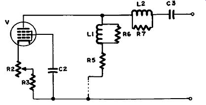
Figure 2.17 Vacuum-Tube Output Circuit
L2 forms a series-resonant circuit (series peaking) with the input capacitance of the following stage, allowing for maximum transfer of signal energy at the upper end of the video spectrum.
By proper choice of inductance values, the two peaking coils can be made resonant over different frequency bands, to extend the amplifier high-frequency response linearly to cover the upper part of the frequency range required.
AC Input Subcircuit (Transistor): Figure 2.18 shows the AC in put subcircuit for the transistor, which is RC-coupled to the previous stage. C1 will have a higher value than its opposite number in the tube circuit as mentioned in our discussion of the audio voltage amplifier.
In this circuit the emitter-bypass capacitor has been left in, so no degeneration will be experienced, except for the very low frequencies (which may be compensated for in another way, as explained in Circuit Variations). In this way, the full gain of the transistor can be realized, an important consideration since it is less than that of a pentode tube.
Operation of the transistor is the same as for the audio voltage amplifier. The output signal is 180° out of phase with the input signal.
Output AC Subcircuit (Transistor): Figure 2.19 shows the output AC subcircuit. C3 couples the output signal to the next stage, and the same considerations apply to the choice of its value as affect the choice of C1.
As in the tube circuit the main concern in the output circuit of the transistor is to avoid attenuation of the high-frequency end of the video spectrum through losses via distributed capacitance.
Shunt-peaking coil L1 forms a parallel-resonant circuit with the distributed capacitance, so as to add to the value of the load resistor
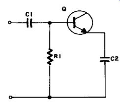
Figure 2.18 Transistor Input Circuit
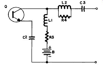
Figure 2.19 Transistor Output Circuit R3 for the higher frequencies for which
it is resonant. The bandpass of this resonant circuit does not have to be broadened
by the addition of a capacitor shunting L1 as the value of R3 is already sufficiently
low to load it enough. Series-peaking coil L2 forms a series-resonant circuit
with the input capacitance of the following stage, allowing maximum transfer
of signal energy at the upper end of the video spectrum. By proper choice of
inductance values the two peaking coils are made resonant over different frequency
bands to extend the high frequency response of the amplifier linearly over
the higher frequencies required.
Circuit Variations
Although the video amplifiers just discussed are typical, you are bound to meet variations in them. However, you will never have any difficulty in identifying a video amplifier (a) because of its position in the overall schematic (between the video detector and the picture tube), and (b) because of the series-shunt peaking coils in the output subcircuit.
One way in which video amplifiers may vary is in the manner in which they provide for low-frequency compensation. You , ve seen one method in the tube circuit. Another method, which is a decoupling circuit, is illustrated in Figure 2.20. In this circuit the value of C2 is such that at high frequencies its reactance is negligible, so that R3 is bypassed and the load resistance consists solely of R2. At low frequencies the reactance of C2 increases until R3 adds to the resistance of R2, which increases the voltage gain for these frequencies, compensating for the losses caused by C1. The values of C2 and C3 must be…
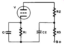
Figure 2.20 Another Type of Low-Frequency Compensation
… chosen carefully to balance out the low-frequency degeneration caused by C1 and R1.
You may be wondering how C2 bypasses R3! Although Figure 2.20 doesn’t show it, the power supply is connected between B+ and the low side of C2 (refer back to Figure 2.12). The large filter capacitors in the power supply offer negligible impedance to signal voltages, so for these frequencies the low side of C2 is to all intents and purposes connected to B+ Because of the cathode-bypass capacitor C1, the contrast control must be located elsewhere than where it was in Figure 2.12. It is often found in the picture-tube circuit instead. However, another way of doing it is shown in Figure 2.21, where bypass capacitor C1 is connected between the cathode and R2, s slider, so that degeneration may be introduced as required to reduce the contrast.
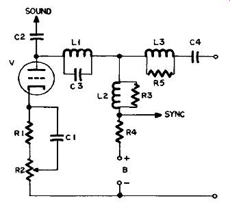
Figure 2.21 Sound and Sync Take-Off
Other variations may be introduced in order to provide for taking of the sound or sync signals from the video amplifier circuit, which is often done. The sound take-of may be from the plate of the tube, which will require the provision of a 4.5-megahertz parallel-resonant trap L1-C3 to block the 4.5-megahertz sound component of the tele vision signal from getting to the picture tube.
The sync signal is usually removed from between the shunt-peaking coil L2 and the load resistor R4, as shown.
IF AMPLIFIERS
IF (intermediate-frequency) amplifiers are voltage amplifiers which handle frequencies very much higher than audio frequencies. Figures 2.22 and 2.23 show IF amplifiers for radio. Figure 2.24 shows one for TV.
Distinguishing Features
IF amplifiers resemble other voltage amplifiers in having grounded cathode or common-emitter circuits.
They are distinguished from other voltage amplifiers by the use of IF transformers to couple into and out of each stage. In Figures 2.22 through 2.24, T1 and T2 are IF transformers.
Uses
All superheterodyne receivers (this includes nearly all modern radio, TV and radar receivers) convert signals of various frequencies picked up by the antenna to a fixed lower frequency, which is then amplified by the IF amplifier. The process of conversion is dealt with in section 5. IF amplifiers are therefore located between the "front end" (tuner-converter section) and the audio or video portions of a receiver.
As you know, audio signal information covers a much narrower range of frequencies than video. For this reason radio IF amplifiers are narrow-band amplifiers, and TV IF amplifiers are wideband.
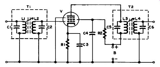
Figure 2.22 Vacuum-Tube IF Amplifier
Detailed Analysis
DC Subcircuit: In all three amplifiers illustrated the DC subcircuits are the same as those of audio voltage amplifiers, except that R1 is replaced by L2, and the current path from the plate or collector to the power source is through L3.
AC Input Subcircuit (Tube): In Figure 2.22 a double-tuned IF transformer T1 couples the input from the previous stage (transformer coupling). The dashed lines surrounding T1 indicate that it is shielded.
The two parallel dashed lines with the arrow, between the coils, show that the coils are permeability tuned, which means that within each coil is a threaded slug of powdered iron that is screwed in or out to tune the resonant circuits L1-C1 and L2-C2 to the intermediate frequency. The symbol for this transformer is different from that of an audio or power laminated iron-core transformer, which would have solid lines and no arrows (see Table 1).
Some types of IF transformers are tuned with variable capacitors instead of variable inductors, but it doesn’t make any difference which type it is as long as it is designed for use at the frequency of the IF amplifier in question.
The signal from the previous stage lows in L1, which is coupled inductively to L2; consequently a voltage is induced in L2. The trans former used in a vacuum-tube circuit is a step-up transformer (more turns on L2 than on L1), so the voltage will be higher across L2 than it was across L1. L2 and C2 form a series-resonant circuit with a resonant voltage step-up across the coil in addition to the transformer step-up, so that the signal has already received a boost before it gets to the tube. This voltage is then applied between the control grid and cathode of the pentode tube, through cathode-bypass capacitor C3.
AC Input Subcircuit (Transistor): In Figure 2.23 T1 is a step-down transformer, and its secondary is tapped so that the low input impedance of the transistor will not load it excessively to the detriment of its selectivity. For this reason transistor-radio IF amplification requires more than one stage as a general rule. The average is two stages for AM and three for FM. A connection through R1 allows AGC voltage (see section 6) to provide the proper bias on the base.
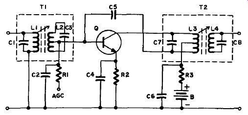
Figure 2.23
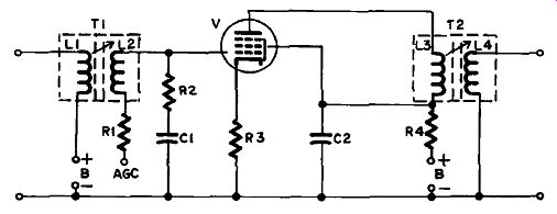
Figure 2.24 Video IF Amplifier
AC Input Subcircuit (Video IF Amplifier): A similar AGC connection appears in Figure 2.24. In this circuit a resistor R2 is connected so that it shunts L2. This broadens its frequency response to enable the amplifier to handle the wider bandwidth of the TV signal.
See how this is exactly the opposite of the radio IF amplifiers, where steps are taken to keep the pass band as narrow as possible. You will also notice that no capacitors are connected across L1, L2, L3 and L4.
At the much higher frequency of the TV IF signal (45.75 megahertz) the distributed capacitance of the circuit is sufficient for the purpose.
In this circuit the cathode-bypass capacitor is omitted also, but be cause R3 is very small the effect on the circuit is not enough to cause degeneration.
AC Output Subcircuit: In the output circuits of all three IF amplifiers L3 forms a parallel-resonant circuit with the shunt capacitance.
The output current from the tube or transistor consists of a DC current with its voltage varying at an IF rate. This current really consists of two currents. One is a steady DC current of constant voltage, which forms the base for the other, which is AC fluctuating at the IF. The DC portion lows through L3 without obstruction, but the AC portion that is fluctuating at the IF encounters a high impedance because the coil has been tuned to be resonant at this frequency. Therefore this portion develops a maximum-signal voltage drop across L3. Any signals of other frequencies, however, do not meet with such an impedance, since they are not at the resonant frequency. Consequently they develop only small voltages. This is what makes this circuit selective for the chosen frequency.
The circuit in Figure 2.22 is one you'd expect to see in a vacuum tube radio. Usually only one IF stage is required. The narrow band width of an AM radio signal (10 kilohertz) or an FM radio signal (150 kilohertz) allows the use of a sharply tuned circuit, which gives maximum amplification when used with a high-gain tube.
In Figure 2.23 the transistor is connected across only part of L3.
This is because the lower output resistance of the transistor acts like a resistor and would broaden the frequency response unduly if connected across the whole winding, to the detriment of good selectivity.
Since the centertap on the coil is grounded for AC through C6, the two opposite ends of the winding will have signals that are 180° out of phase with each other. A connection from the lower end of the coil goes via C5 to the base of Q. This places a signal on the base which is of opposite phase to the collector signal, and serves to cancel any feedback through the transistor that might cause oscillation. (The same precaution would have to be taken with a triode tube, but is not required with a pentode because the screen grid--at AC ground potential--prevents feedback from the plate to the grid.) In Figure 2.24 the shunting capacitor across L3 has been omitted because the distributed capacitance is sufficient for the purpose. The loading effect of R4 in series with L3 broadens the frequency response enough for video IF amplification.
Because of the reduced amplification resulting from loading the IF transformers, video IF amplifiers require more than one stage (usually three for tubes). In a three-stage IF amplifier there will be four IF transformers. These will be stagger-tuned. This means that instead of all four being tuned to the same frequency, they will be tuned to different portions of the 4-megahertz bandwidth of the video signal.
For example, the four frequencies might be 43.1, 43.5, 44.2 and 46.0 megahertz (they will differ slightly in different models of TV sets), which would combine in the overall picture to cover frequencies from 41.75 to 45.75, the difference of 4 megahertz required. These frequencies are usually shown on the schematic of the IF amplifier beside each IF transformer. When the picture-carrier signal is removed in the demodulator stage only the 4-megahertz band of video frequencies will remain, as explained in section 6.
RF AMPLIFIERS
RF amplifiers used in receivers are voltage amplifiers, having circuits similar to the voltage amplifiers described in the preceding portion of this section. In fact, RF pentode amplifiers are the same as IF pentode amplifiers, except that the input is from an antenna and tunable resonant circuit.
Most RF amplifiers in use today will be found in TV and FM tuners.
For this reason Figure 2.25 shows an extremely popular type of TV circuit, and Figure 2.26 a typical solid-state FM circuit.
Distinguishing Features
In Figure 2.25 you see an RF cascode amplifier. This circuit uses a dual-triode tube (two tubes in one envelope). The antenna and tunable resonant circuit in the input tell you it handles RF. The first triode section is connected in a grounded-cathode circuit, as in other voltage amplifiers. The second is connected as a grounded-grid amplifier. In the output from the second tube section is a transformer (tunable to each TV channel) which couples the signals into the next stage.
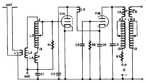
Figure 2.25 RF Cascode Amplifier
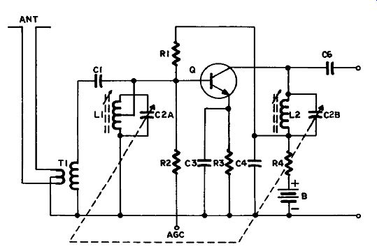
Figure 2.26 RF Transistor Amplifier
In Figure 2.26 the input from the antenna and tunable resonant circuit is applied to the base of the transistor, from which you know that this circuit must also be handling RF. It is connected in a common emitter circuit, with another tunable resonant circuit in the output, after which the signal is capacitor-coupled into the next stage.
Uses
Cascode amplifiers are used extensively in TV tuners. The gain from the dual-triode is approximately the same as that from a single pentode, but the noise level is very much lower. However, triodes are susceptible to oscillation at very high frequencies, which has to be prevented by careful design. Pentodes were used in some older circuits before the dual-triode was developed. The two triodes in the dual triode are shielded from each other by a screen which is grounded.
Transistors also may be used in TV tuners and modern FM radios.
RF amplifiers are seldom used in AM radios, except in some auto mobile models. But they are used extensively in communications receivers. In any receiver the RF amplifier will be in the first stage or stages.
Detailed Analysis
DC Subcircuit (Vacuum Tube): In Figure 2.25 electron low is from B- to the cathode of V1A, thence to the plate, and via L5 to the cathode of V1B. From V1B’s plate the low is through L6, L7 and R3 back to B+. Grid bias on V1A is supplied by AGC voltage (see section 6).
DC Subcircuit (Transistor): In Figure 2.26 electron low is from B- through R3 to the emitter, through Q to the collector, thence through L2 and R4 back to B+. In a PNP transistor, with polarities reversed, the low would be in the opposite direction. The bias across the emitter-base junction is stabilized by R1 and R3. AGC voltage is supplied via R2.
Input Subcircuit (V1A): The signals picked up by the dipole antenna are inductively coupled from L1 to L2 (Figure 2.25). This is a balun transformer, since it couples the balanced line from the antenna to the unbalanced amplifier circuit. (The amplifier circuit is said to be unbalanced because it has a high and low side.) The RF signals then are applied across L3 and L4, of which the upper end is connected to the grid of V1A and the lower end to the low side of the circuit via C1. L3 and L4 are the antenna section of the TV tuner, which may be a turret tuner or a rotary tuner. The sliding contact represented by the arrow selects the desired channel by shorting out more or less of L3.
At the Channel 2 tap all the inductance is in the circuit; at the Channel 13 tap only L4 is left in. L4 is adjustable for touching up the overall tuning when necessary (when a tube is changed in the tuner, for example). The tuning coils L3 and L4 form a resonant circuit with the distributed capacitance of the circuit-mainly in the tube-which applies a maximum voltage between grid and cathode for the selected channel, while attenuating all the others. R1 broadens the tuning enough to give the wide pass band (about 6 megahertz in the tuner) required for the TV signal.
Output Subcircuit (V1A) and Input Subcircuit (V1B): The output of V1A is developed across V1B, which is its load resistor, as it were.
This is a fairly low resistance, so there is no danger of oscillation in V1A. (Oscillation requires a strong signal in the output to give enough feedback.) Unwanted higher frequencies are blocked by L5, and de coupled by C2.
The signal is applied between the cathode and grid of V1B. Since the grid is connected to the low side of the circuit through C3, this is a grounded-grid amplifier circuit. The gain is not as high as in a grounded-cathode amplifier, but the grounded grid blocks feedback from the plate to the cathode, thus preventing oscillation.
Output Subcircuit (Figure 2.25): The output of V1B is applied across the RF tuning coils L6 and L7, and coupled by transformer action to L8 and L9. Tuning L7 and L9 is performed simultaneously with L3, all three moving contacts being connected to the same tuning control. R3 in series with L7 broadens the response in the same way as R1 does.
Input Subcircuit (Figure 2.26): The signals picked up by the dipole antenna are inductively coupled via the balun T1, and are then applied across the resonant circuit L1-C2A. The signal of the frequency to which the circuit is tuned is then applied between the base and emitter of Q.
Output Subcircuit (Figure 2.26): The output of Q is applied across the RF tuning coil L2, which is tuned to resonance by C2B. This vari able capacitor is ganged with C2A (as indicated by the dashed lines) so that both input and output circuits are simultaneously tuned to the same frequency. The output signal is then coupled into the next stage through C6.
-----------------
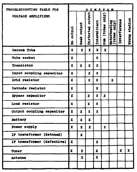
troubleshooting table for VOLTAGE AMPLIFIERS
-------------------