THE SIGNALS USED IN electronic circuits usually have to be tailored to fit the purpose for which they are required. This tailoring is done with a variety of standard circuits which reduce the amplitude, change the shape, separate, or otherwise modify a signal.
Attenuators and Pads
The distinguishing feature of attenuators and pads is that they consist of resistors. Attenuators are resistive networks that reduce the strength of a signal without introducing appreciable distortion. A pad is a resistive network that attenuates a signal without introducing an impedance mismatch. It is also used to match dissimilar impedances to avoid unnecessary signal attenuation, in which case it is called a minimum-loss pad.
Fixed pads are either symmetrical or asymmetrical. In the first the input and output impedances are the same, in the second they are not.
They are also balanced or unbalanced, depending upon whether the two sides are alike or unlike with regard to a common reference (usually ground). This means that an unbalanced pad is one with one side grounded or at zero potential, as in most circuits, while a balanced pad has neither side grounded.
In Figure 8.1 the first unbalanced pad is called an L-pad because the arrangement of its resistors resembles an upside-down L. Its balanced counterpart is a U-pad, because it looks like a U lying on its side. The resistors drawn horizontally are series resistors; the vertical are shunt resistors. These are impedance-matching pads, and are also called minimum-loss because they do not cause much attenuation.
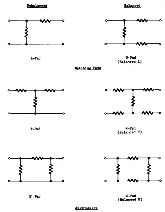
Figure 8.1 Fixed Pads
The next unbalanced pad is a T-pad, and its balanced version is an H-pad. These pads are used for attenuation. They should be connected between similar impedances.
The bottom two pads are also for attenuation, not for impedance matching. The pi-pad, like the pi-filter, is named for its resemblance to the Greek letter it (pi).
Figure 8.2 shows T and H pads with resistors shunted across the series resistors. They are called bridged-T and bridged-H pads.
Variable pads are also illustrated in Figure 8.2. These are designed so that the attenuation can be varied while maintaining the impedance match. In a simple potentiometer the amount of resistance shunting the device connected to it varies with the setting. In the examples shown, one resistor increases as the other decreases to maintain a constant impedance.
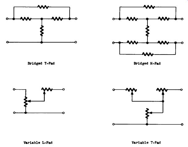
Figure 8.2 Bridged and Variable Pads
Filters
A filter is a selective network designed to pass signals within a certain frequency range ("pass band"), while attenuating those of other frequencies. Filters are categorized as low-pass, high-pass, bandpass and bandstop. The distinguishing feature of all of them is the use of inductor-capacitor (L-C) circuits. A low-pass filter passes lower frequencies but attenuates higher ones. Figure 8.3 shows six low-pass filters. They look somewhat like the pads in Figure 8.1, except that all are unbalanced. In each there is a series inductance and a shunt capacitance. The inductance has more reactance to higher frequencies, while the capacitance has more reactance to lower ones. Consequently, higher frequencies find an easier path through the capacitance, and so are bypassed, but the inductance offers less reactance to the lower frequencies which therefore are not bypassed.
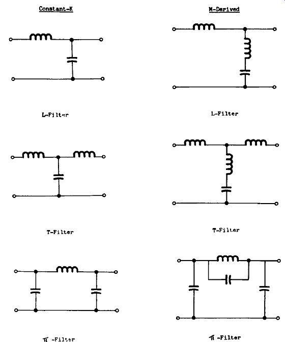
Figure 8.3 Low-Pass Filters
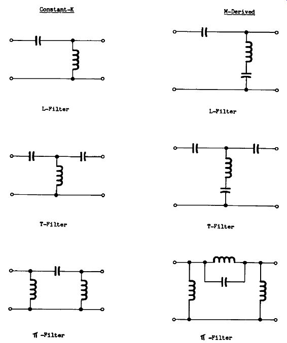
Figure 8.4 High-Pass Filters
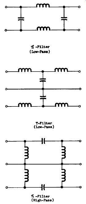
Figure 8.5 Balanced Filters
Constant-k filters are simpler than m-derived filters, and do not have as sharp a cutoff. For many purposes this is no disadvantage. The power supplies discussed in section 7 make extensive use of low-pass filters, especially filters to eliminate 60- and 120-hertz AC, while passing DC (which in this connection can be regarded as ultra-low frequency AC).
In the m-derived filters the addition of shunt inductances in the first two makes, with the shunt capacitance, series-resonant circuits having a very low shunt impedance to frequencies just below the cutoff frequency. This results in a steep drop in the frequency response below the cutoff frequency. The circuit in the third filter is a parallel-resonant circuit, and so offers a high series reactance to frequencies below cutoff.
A high-pass filter passes higher frequencies but attenuates lower ones. Figure 8.4 shows six high-pass filters. They are the counterparts of those in Figure 8.3. In each one there is a series capacitance and a shunt inductance. The lower frequencies find an easier path through the inductance, and so are bypassed, while the capacitance offers much less reactance to the higher frequencies, which are not bypassed.
The distinctions between k- and m-derived filters are also similar to those that apply to low-pass filters.
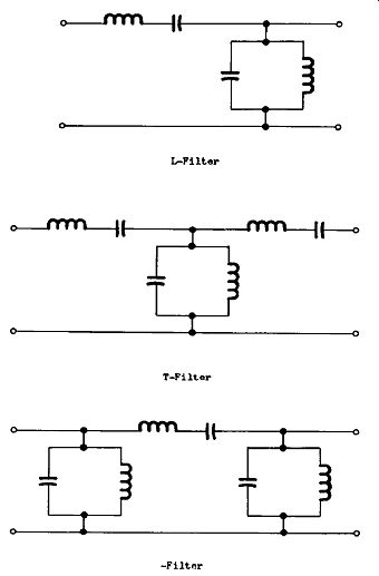
Figure 8.6 Bandpass Filters
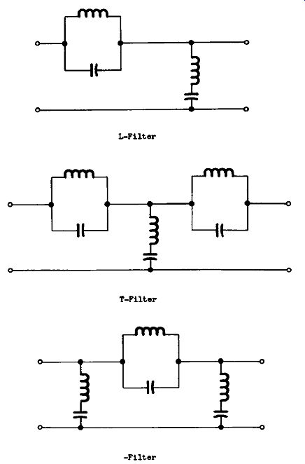
Figure 8.7 Bandstop Filters
The filters in Figures 8.3 and 8.4 were unbalanced filters. Examples of balanced versions are shown in Figure 8.5.
Bandpass filters allow signals with the desired frequency to pass while rejecting all others. The width of the band depends on the selectivity of the circuit, which can be made broader by increasing the resistance in it. Figure 8.6 illustrates three typical bandpass filters of the constant-k type. They resemble the unbalanced pads shown in Figure 8.1, with series-resonant circuits substituted for the series resistors and parallel-resonant circuits replacing the shunt resistors. Series resonant circuits offer a very low reactance to signals at and near the resonant frequency, but parallel-resonant circuits are the opposite. To signals of other frequencies the series-resonant circuit offers a much higher reactance, the parallel-resonant one much lower. Consequently signals within the pass band find an easy path along the upper part of the circuit, and are not bypassed, while other frequencies are severely attenuated.
Bandstop filters are illustrated in Figure 8.7. If you compare this with Figure 8.6 you will see that they are counterparts. The series and parallel-resonant circuits have changed places. As a result, bandstop filters discriminate against the selected frequency instead of favoring it.
Integration and Differentiation
The two circuits in Figure 8.8 each consist of a capacitor and resistor only, which is what distinguishes them from the attenuators and filters we've just considered.
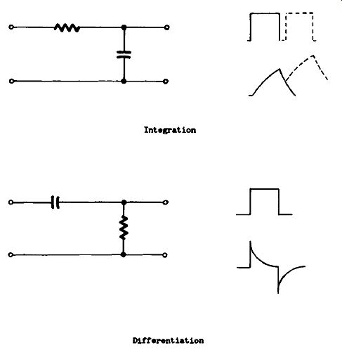
Figure 8.8 Integration and Differentiation
An integrator consists of a capacitor charging through a resistor.
Its output represents the time integral of its input or, in other words, the output voltage is proportional to the time constant of the R-C combination. When a pulse with a waveform similar to the upper out line is applied to the input it is changed so that the output waveform is like the lower outline. This happens because the capacitor cannot charge instantly to the voltage of the pulse, but must build up the voltage at a rate determined by the low of current through the resistor.
This circuit is used in television receivers to build up a voltage to trigger the vertical oscillator by accumulating the vertical synchronizing pulses that occur between each field (frame). These pulses have a long duration compared to the time interval between them, so that each pulse adds its voltage to that of its predecessor before the capacitor has had time to discharge, as shown in the dashed outlines in Figure 8.8.
Integrators are used in a similar way in counters, frequency dividers and the like. They may be compared to low-pass filters.
A differentiator, on the other hand, resembles a high-pass filter.
This circuit consists of a capacitor and resistor arranged as shown.
When a voltage is applied to the input, current lows to charge both sides of the capacitor. As the capacitor has no charge at first, the initial current is high, tapering of as the capacitor becomes charged.
This current lowing through the resistor produces a corresponding voltage drop that has the waveform shown, with a sharp positive-going spike initially when the leading edge of the pulse arrives, and a negative-going spike, caused by the discharge current, at the pulse trailing edge.
In television receivers this circuit serves to change the vertical synchronizing pulses into sharp triggering pulses to maintain horizontal synchronization during the period between fields when these extra wide pulses are being received.
Clippers (Figure 8.9) may be either series or shunt. The distinguishing feature is a diode. Those shown in the figure are semiconductors, but vacuum-tube diodes could be used in the same way. These diodes have been biased by placing a DC source where it applies a reverse bias to the diode, such that this voltage has to be overcome before the diode can conduct.
In the series-clipper, current can low through the diode whenever the anode voltage is positive with respect to the cathode (the right hand side of the diode symbol, with the line). The DC source biases ...
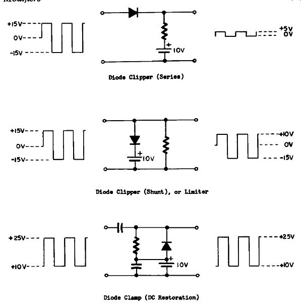
Figure 8.9 Clippers, Limiters and Clamps --- Diode Clamp (DC Restoration)
---- Diode Clipper (Shunt), or Limiter --- Diode Clipper (Series)
... the cathode with a positive 10 volts. Consequently the diode can only conduct when the voltage on its anode exceeds 10 volts. If a square wave with positive and negative excursions (peaks) of 15 volts is applied to the input, the diode will conduct only during that part of the positive excursion that exceeds 10 volts, which is 5 volts. This gives an output of 5-volt pulses as shown. The rest of the input is blocked by the diode, and is said to have been clipped.
The shunt clipper has also been biased with 10 volts. A negative excursion of the square wave is not bypassed, as the diode does not conduct; consequently the whole negative 15 volts appears at the output. The diode does not conduct until more than 10 volts of the positive excursion appears on the anode of the diode. Voltage above this is bypassed, therefore only 10 volts of the positive excursion appears in the output.
The shunt clipper when used with a pulse train is also a limiter, since by clipping all the pulses to the same height, variations in amplitude (transients, overshoots, noise, etc.) can be removed. The series clipper does not do this, as in its case the bottom of the pulse is removed instead of the top.
The action of a clipper is the same for sine waves as for square waves. In fact, a sort of square wave can be produced by cutting off the tops of sine waves.
Reversing the polarity of diode and bias reverses the polarity of the clipping.
Clamp circuits are used for DC restoration. In the circuit shown in Figure 8.9 a train of pulses with voltage alternating between +25 volts and +10 volts is coupled through a series capacitor. This signal is equivalent to a train of 15-volt pulses riding on a 10-volt DC base.
The capacitor cannot pass the DC portion, so only the train of pulses appears across the resistor.
The missing DC is restored by the DC source, which replaces the 10 volts that could not pass through the capacitor. This voltage is present on both sides of the diode. When a pulse arrives the voltage on the cathode increases to +25 volts; the diode does not conduct as its anode is still at 10 volts. However, any negative overshoot which takes the cathode below +10 volts causes the diode to conduct, and the overshoot is bypassed. In this way the pulse train is clamped to a 10-volt base.
If the DC source is omitted the pulse train will be clamped to a zero base. Other DC voltages may also be used. The shunt capacitor is provided to bypass the DC source so that no signal voltage is dropped across it.
-------------------