CONTROL CIRCUITS ARE widely used in industry. In this category are found the logic circuits in computers, gating, inverting and inhibiting circuits. Many of these circuits used to employ relays (and equipment using relays will be around for years) but today transistor and diode switches are used extensively because of their smaller physical size and generally greater reliability. Large electronic computers require thousands of simple on-off switches that can be operated by pulses at extremely high speeds.
Logic Circuits
Modern computer switches must operate at microsecond speed. No mechanical device can do this, hence the use of semiconductors.
A diode or transistor (which is really two diodes back-to-back), when used as a switch, has two states. In its of state its resistance is several megohms, in its on state its resistance may be as low as 50 milliohms. In this respect it is superior to a vacuum tube, which has an internal resistance of approximately a kilohm, when conducting, so that it dissipates power. It also requires current for its heater.
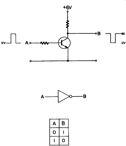
Figure 9.1 NOT Gate, or Inverter.
The semiconductor is switched from one state to the other by changing the bias voltage from forward to reverse, and vice-versa. The voltage required to do this is quite small, and is usually in the form of a pulse.
Various types of logic circuit have been designed. Transistors are used more than diodes, because they also amplify, so that they can compensate for circuit losses.
NOT Gate, or Inverter Figure 9.1 illustrates a NOT gate, or inverter. As you can see, it is a simple common-emitter amplifier. If the supply voltage is positive (with a PNP transistor, as shown) it requires a positive voltage on the base to make it conduct.
Without a positive voltage on the base the transistor-switch is of, therefore the voltage at B will be the same as the supply voltage. When a positive voltage pulse arrives at A it turns the transistor-switch on, so that B is now approximately at zero potential, giving a negative pulse output. Since this is the opposite of the positive-pulse input the device is an inverter.
The pulse that turns a switch on is called true. The absence of such a pulse (which turns it of) is called false. A table showing the operation of the switch with different inputs is called a truth table. In it the true signal is indicated by a figure 1, the false by a figure 0. The actual voltage of the signal may be anywhere from 2 to 12 volts, depending on whether diode or transistor circuitry is employed.
In the truth table in Figure 9.1 the false signal at A gives a true output at B, which means, in this case, that no input at A gives a +6 volt output, because the transistor is cut of. When a true signal is received at A the voltage at B drops to zero, which is a false output.
As you can see, a true input gives a false output and a false input gives a true output. Thus the device is called a NOT gate because its output is not the same as its input.
The triangular symbol represents the device in logic diagrams. It is nearly always called an inverter.
AND Gate
Figure 9.2 shows an AND gate. The transistors Q1 and Q2 are connected in series, so that both have to turn on before current can low through them. The collector of Q1 remains at the supply voltage until true signals are received at both A and B, when it drops to approximately zero. This turns Q3 of, and the voltage at C rises to the value of the supply voltage (Q3 is an inverter). The effect of different inputs is shown in the truth table.
This device is not used very much any more, but serves as the basis for others, as we shall see. Note the symbol.
OR Gate
The OR gate in Figure 9.3 is activated by a true input at either A or B, since the transistors are in parallel. When both transistors are of, the voltage at C will be zero. When either or both turn on, current lowing through R2 causes the voltage at C to rise approximately to the value of the supply voltage. Consequently a true input at either A or B gives a true output at C, as shown in the truth table.
This is another basic circuit seldom used as shown. Note the symbol.
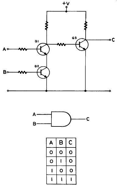
Figure 9.2 AND Gate
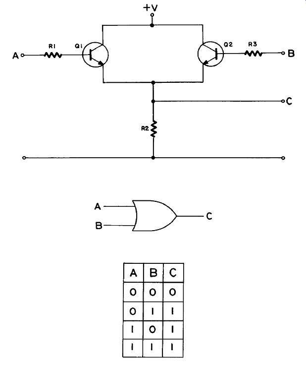
Figure 9.3 OR Gate
RTL NOR Gate
A NOR gate is an OR gate with a reversed output. In Figure 9.4 the OR symbol now has a small circle added, which indicates the inversion. This could be done by adding the inverter of Figure 9.1. however, in this case, by taking the output from the collectors of Q1 and Q2 an inverted output is also obtained, as shown in the truth table.
This is one of the most widely used gates. RTL stands for resistor transistor logic.
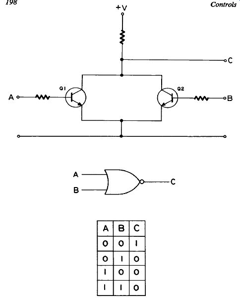
Figure 9.4 RTL NOR Gate
DTL NAND Gate
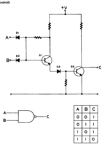
Figure 9.5 DTL NAND Gate
A NAND gate (Figure 9.5 ) is an AND gate with a reversed output.
Note that the AND symbol now has a small circle added, which indicates the inversion. DTL stands for diode-transistor logic.
As long as either diode can conduct, Q1's base voltage is low, and Q1 is cut off. As Q1’s emitter is at zero potential (with no current lowing through Q1) Q2 is also cut of. When true signals appear at A and B both diodes are reverse-biased and cannot conduct. Consequently Q1 , s base voltage rises, turning Q1 on. The voltage drop across Q1's emitter resistor turns Q2 on, resulting in a false output at C.
TTL NAND Gate
The TTL (transistor-transistor logic) NAND gate (Figure 9.6) is also widely used. It has a higher speed of operation than the DTL.
Q1 is a special transistor with two emitters (multiple-emitter transistor). When either or both emitters have a false input Q1 is cut of.
The output from Q1's collector is essentially zero. As a result Q2 is also cut of. The voltage on Q2's emitter is zero, that on its collector the same as the supply voltage. In other words, with a false signal on its base Q2 has two outputs: false from the emitter, true from the collector. Q2 is therefore a phase-splitter.
Q3 and Q4 are connected in series (a "totem pole"). When Q2's collector is true the base of Q3 is true also, so Q3 is turned on. At the same time Q4 is turned of by the false signal from Q2’s emitter. As a result the collector of Q4 is at the supply voltage (all the voltage is dropped across Q4), and the output at C is true.
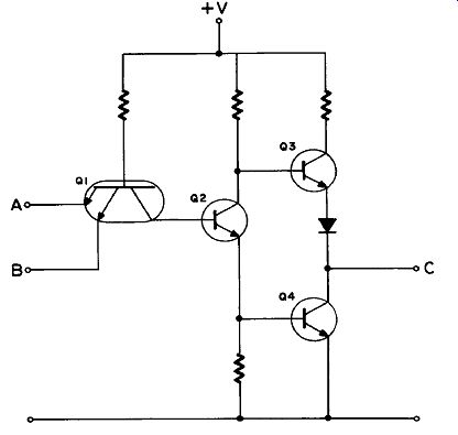
Figure 9.6 TTL NAND Gate
When true signals are applied simultaneously to A and B Q1 turns on. This places a positive (true) voltage on the base of Q2, so its two output signals are now the opposite of what they were before. Consequently Q3 turns of and Q4 turns on. Now a false (zero) output appears at C.
The truth table and symbol for this circuit are the same as in Figure AND, and OR Gates from NAND and NOR Since the NAND and NOR gates just described are used for practically all logic circuits today, the older AND, and OR gates are seldom seen. To get an AND or an OR gate the usual procedure is to add inverters to the output or input, as shown in Figure 9.7. In this way a NAND gate can be converted to an AND or an OR gate; similarly, with a NOR gate. In this way the same type of gate can be used throughout an entire digital system.
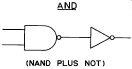
Figure 9.7 AND Gate Used Today
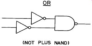
Figure 9.8 OR Gate Used Today
The most popular type is the NAND gate. See also Figures 9.8,
(NOR PLUS NOT)
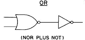
Figure 9.9 OR Gate Used Today AND (NOT PLUS NOR)
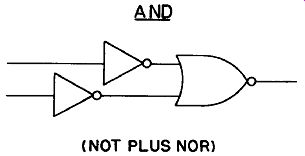
Figure 9.10 AND Gate Used Today Combining Circuits
It is often necessary to combine or mix two or more different inputs, such as the audio from two microphones. The circuit in Figure 9.3 becomes a combining circuit with the addition of a cathode-bypass capacitor parallel to R2. The two signals to be combined are fed in at A and B, of course, and as their levels will probably require adjusting, volume controls are usually provided for each input.
Gating Circuits
A circuit such as that in Figure 9.6 can also be used to gate a signal;
that is to say, to turn it on and off. Suppose a train of positive pulses is applied to input A. Nothing will happen, because input B is still false.
But if a true signal voltage is now applied at B, each pulse at A will turn Q1 on, so that a train of inverted pulses appears at C. This will cease when we remove the true voltage at B.
Obviously, any NAND gate can be used in this way.
Inhibiting Circuit
Figure 9.11 shows an inhibiting circuit. An inhibiting circuit's function is the opposite of a gating circuit. The inhibiting signal cuts of the other signal by canceling part of it. T1 is a phase-reversing transformer.
If the two signals at A and B have the same phase, they will be of opposite phase on the base of Q1. If they are of the same amplitude, cancellation will take place as shown. The residual signal is reversed again to appear at C with the same phase as at B.
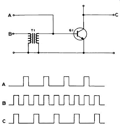
Figure 9.11 Inhibiting Gate
Integrated Circuits
It is now possible to make complete circuits on a very small scale, and many have been standardized for mass-production.
Such circuits are called integrated circuits (ICs). Among them are many logic circuits, of which the following one is a typical example.
Figure 9.12 is ail outline diagram of such a device. Its actual size, ignoring the leads, is a fourth of an inch long and a twentieth of an inch thick. This is a standard "package" with fourteen leads, numbered as shown. Packages may have fewer or more leads, but they are always numbered counterclockwise when viewed from above. The block dia gram does not appear on the device itself, of course. It appears that way in the manufacturer’s catalog to show the lead connections.
ICs come in other shapes and sizes as well. Some resemble transistors, except for the larger number of leads. All are very small, and completely encapsulated in ceramic, plastic or metal.
The circuit on the outline diagram in Figure 9.12 is represented by the symbols for two AND gates, with inputs C1( C2 and S1, S2, and a rectangle with inputs CP (clock pulse), outputs Q and Q ( " NOT-Q" or inverted Q), Sd (direct set-pulse) and Cd (direct clear-pulse). This is enough to tell us that this circuit is controlled by a clock pulse. In puts will only be accepted while the clock pulse is present at pin 2.
Texas Instruments
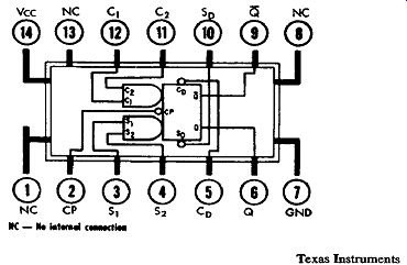
Figure 9.12 Integrated Circuit
This means that with true inputs at C1 and C2 the clock pulse switches the circuit to give a false output at Q and a true output at Q. True inputs at Sx and S2 give a true output at Q and a false one at Q. These are shown in the truth table in Figure 9.13, which also shows that other inputs have no effect, or an indeterminate one.
However, an input at Sd overrides the clock pulse, and sets the device to give predetermined true and false outputs at Q and Q as long as the preset voltage is maintained. An input at Cd does the same, except that the outputs are reversed.
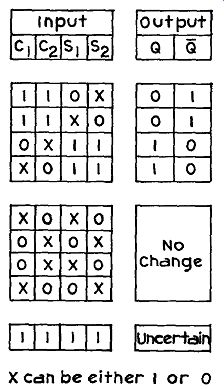
Figure 9.13 Truth Table of IC
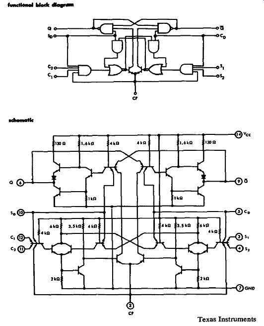
Figure 9.14 gives the complete functional block diagram for the circuit. You
should have no difficulty in identifying the various logic symbols, as they
were explained earlier in this section. The two transistors directly above
the clock-pulse input are also controlled by the pulse, which turns them on
to allow the input signal to pass to the input output section. A true input
at Q and C2, as we have already seen, passes via the AND gate to the NOR gate,
then via the adjacent transistor to the left-hand NAND gate, and appears as
a false signal at Q.
At the same time part of this output goes across to the right-hand NAND gate and lips it to give a true signal at Q. This chain of events happens in the right-hand half of the circuit with true inputs at S1 and S2, except that the outputs are reversed.
Figure 9.14 Functional Block Diagram and Schematic of IC
Figure 9.14 also gives the complete schematic for the circuit. Notice that the transistor symbols do not have circles round them. The circles are optional, and some schematics omit them, like this one.
You will see several multi-emitter transistors similar to that you met with in Figure 9.6. The DC operating voltage (5 volts) comes in at pin 14 (Vcc), and the return is from pin 7, which you can see is connected to the low side of the circuit.
See if you can identify the various circuits. It's not as difficult as it looks if you refer back to the examples given earlier in the section.
(Hint: the multi-emitter transistors connected to pins 11 and 12, and pins 3 and 4, are the AND gates.) This is a high-speed switching circuit. Typically, the clock-pulse frequency would be 15 megahertz, and the time required for true inputs at Q and C2 or Si and S2 to switch through to the output would be 25 nanoseconds.
-------------------