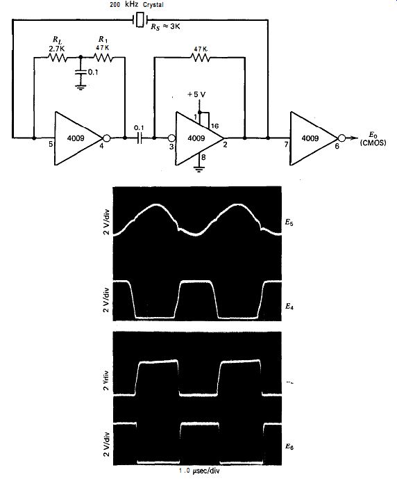
Figure 11.1. CMOS Two-Inverters (4009) circuit at 200 kHz.
| Home | Audio mag. | Stereo Review mag. | High Fidelity mag. | AE/AA mag. |
This section contains performance test data on individual IC oscillator circuits. It is divided into five parts, the first of which describes oscillator characteristics of various IC technologies and gives some general characteristics of various IC oscillator types. The second part covers series resonant circuits, and the third covers Pierce circuits. Special oscillator ICs are discussed in the fourth part, and a VHF harmonic oscillator in the fifth.
A. CIRCUIT SELECTION
The basic principle in selecting IC oscillator circuits was to try as many types and kinds of ICs as possible, testing each one to find its strong and weak points. A total of 24 different IC oscillator circuits were built and tested, using ECL, TTL, CMOS, and LINEAR technologies. Eight were series-resonant circuits, six were Pierce circuits, and one was a VHF harmonic circuit. Nine more were special ICs, specifically designed to be used as crystal oscillators.
The search for a good IC that a quartz crystal would like was mainly for a circuit with linear input and binary (square wave) output. A gain of 2-60X was needed, the exact amount depending on the circuit used.
Line receivers and voltage comparators have linear-input resistances and binary outputs, making them potentially good choices.
In general, TTL does not work too well in an oscillator circuit, be cause its input resistance is highly nonlinear at the switching point, and it exhibits bad parasitic oscillations if it does not switch rapidly between
its two binary output states. CMOS has good input characteristics, but it is pretty limited in its output-drive capability. In contrast, ECL is almost ideal for an oscillator circuit, with its high linear input resistance and low output resistance, combined with a good output-drive capability.
Some of the IC oscillator circuits tested were not TTL or CMOS compatible. Level shifters or buffers were added to these circuits to make them TTL compatible. After selection, each circuit was individually optimized by test for the best component values, bias, waveforms, and so forth. The ICs used have a strong effect on circuit performance, so considerable time was spent selecting the right one for each circuit. Most of the optimizing of the fundamental circuits was done at 1 MHz, and photographs were taken of waveforms at various points in the circuits.
Just as with the discrete transistor circuits, waveform photographs were synchronized to a common point in time and vertically aligned together on the printed page. This permits vertical waveform comparisons at the same point in time between various parts of a circuit.
The same test philosophy was used in testing integrated circuits that was used in testing discrete transistor circuits. That test philosophy is described in Section IOA and will not be repeated here.
B. SERIES RESONANCE
11.1. CMOS TWO-INVFBTERS-4009
The schematic of this series-resonant oscillator at 200 kHz is shown in Fig. 11.1. This circuit is a variation of the TTL inverter oscillator shown in Fig. 11.3~. Because of the longer time delay in a CMOS inverter, this CMOS version is restricted to frequencies below 300 kHz. The CMOS inverter used is the 4009, a high-current driver with a short internal time delay. There is a large variation in this inverter's time delay among different manufacturers. The RCA 4009 had the shortest time delay of any of the brands tested and is recommended.
Each inverter in Fig. 11.1 has negative feedback around it to ensure that it is biased in the middle of its linear region, so that oscillation will always start when power is applied. The feedback resistor around the first inverter is divided into two series resistors, and the center point is bypassed to ground. R, is used as the crystal's load resistor and set equal to or somewhat less than the crystal's internal series resistance R,.
Figure 11.1. CMOS Two-Inverters (4009) circuit at 200 kHz.
Figure 11.1 shows good waveforms at the crystal. The small spikes on the crystal's sine wave output appear to be due to the sharp edges of the crystal's square wave drive feeding through on the crystal's shunt terminal capacitance CO.
The overall performance of the 4009 inverter circuit is poor, because its frequency is much too sensitive to changes in power supply voltage and ambient temperature.
11.2. CMOS TWO-INVERTERS-74C04
The schematic of this series-resonant circuit at 200 kHz is shown in Fig. 11.2. The purpose of this circuit is to see if the 74C series works any better than the 4000 series, and the answer is yes, it does. The circuit in Fig. 11.2 is the same as the 4009 circuit in Fig. 11.1 except for the substitution of the 74C04 for the 4009. The 74604 will oscillate at a higher frequency (up to 500 kHz, as compared with 300 kHz for the 4009), and it is less sensitive to temperature changes.
As in the 4009 circuit, the crystal's load resistance RL is set equal to or somewhat less than the crystal's internal series resistance R,. Figure 11.2 shows good waveforms at the crystal. The spikes on the crystal's sine wave output appear to be due to sharp edges of the crystal's square wave drive feeding through on the crystal's shunt terminal capacitance Co.
The overall performance of the 74604 inverter circuit is below aver age, because its frequency sensitivity to power supply voltage changes is higher than it should be. This high sensitivity to power supply voltage changes seems to be characteristic of most CMOS ICs.
11.3. TTL TWO-INVERTERS-7404
The schematic of this series-resonant oscillator is shown in Fig. 11.3.
Many versions of this circuit are poorly designed; credit for this properly designed version of the TTL inverter circuit goes to S. D. Culp [19]. The circuit gives good performance. Crystal waveforms are fairly good, and the frequency is relatively insensitive to power supply and temperature changes. This circuit, in its many variations, is one of the most widely used TTL oscillator circuits.
The circuit uses two negative feedback schemes to ensure oscillation start-up when power is applied, one on each inverter. The circuit will work with any standard TTL NAND gate, NOR gate, or inverter. The output of each gate (or inverter) must be the negative of its input, so that negative feedback can be used to bias the input and ensure oscillator start-up. This subject is discussed in detail in Section 9.
The negative feedback. on the second inverter in Fig. 11.3~ is the simplest, consisting of the single resistor R,. Although it does not hurt the second inverter, the single resistor feedback method has the disadvantage of reflecting back a highly nonlinear load resistance to the input (pin 3) of the inverter. A 'ITL inverter has a gain of approximately 10X.
During transition intervals, the 470-ohm resistance of the feedback resistor R2 is reduced to 47 a, as seen at the inverter's input (pin 3). At either of the binary states "0" or "1," amplifier gain is effectively zero, so the input impedance of the 470-R feedback resistor is then 470 ohm instead of 47 R. Such a highly nonlinear load on the amplifier input, switching back and forth between 470 and 47 R, is undesirable as a crystal load and it should not be used on the first inverter because of distortion introduced on the voltage output from the crystal.
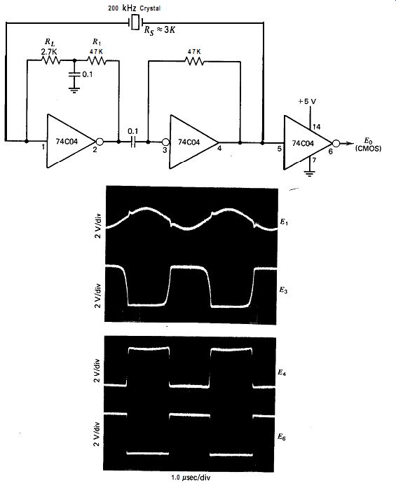
Figure 11.2. CMOS Two-Inverters (7404) circuit at 200 kHz. (74C04 Copyright
1981 National Semiconductor Corporation.)
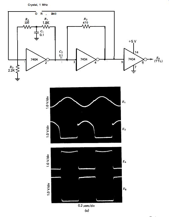
Figure 11.3(a). TTL Two-Inverters (7404) circuit at 1 MHz. Set RL = R, (RL
+ R,) = 2KR.
The negative feedback around the first inverter is arranged differently. Here, the feedback resistor is divided into two resistors RL and RI, and the center point is bypassed to ground with a capacitor. The resistance of the feedback network reflected back to the crystal is then constant over a complete waveform cycle and equal to RL. The improvement in the crystal's output waveform by adding the bypass capacitor C 1 in the middle of the two feedback resistors R, and RI is quite significant.
The input (pin 1) of the first inverter is also tied to ground by a resistor RS. This shunt resistor R, has two functions. First, it pulls the inverter's input into the transition region, so that both the input and output of the inverter are somewhere near +1.6 VDC. The two feedback resistors (R, and R,) then provide additional negative feedback at low frequencies to stabilize the inverter's output voltage (pin 2) at +1.6 VDC, the binary switching point. The second function of R, is to control the on/off ratio of the oscillator's square wave output. Adjusting the value of R3 (+30% ?) will trim the square wave output to a perfect 50/50 on/off ratio. The capacitor C2 between the two inverters is used for DC isolation and al lows them to be independently biased without interaction.
The small spikes on E_1 in Fig. 11.3a are high-frequency edges of the crystal's square wave drive, which are feeding through the crystal on its terminal shunt capacitance C_0. There are flat spots adjacent to the switching spikes on the crystal's output voltage E ,. These flat spots indicate that the input resistance of the inverter itself becomes very low during these flat-spot intervals. These nonlinear, low-resistance flat spots in E_1 occur at the worst possible place in the cycle, that is, at the switching point. They increase timing uncertainty as to when the inverter will switch from one binary state to the other and degrade the circuit's short-term frequency stability.
Figure 11.3b shows the inverter circuit with the 74804 instead of the 7404, and Fig. 11.3~ shows the inverter circuit with the 74LS04. The 74LS04 is the most useful of the three inverters because it covers a wider frequency range than the other two. The 74LS04's higher input resistance allows the use of larger feedback resistors. This permits a higher crystal load resistance R,, which is needed for operation at lower frequencies. The 74LS04 will operate down to 100 kHz, whereas the 7404 will operate down to only 800 kHz, and the 74S04 down to 1 MHz. Dissipation in the crystal limits the highest oscillation frequency to about 3 MHz in all three circuits.
11.4. TTL VOLTAGE COMPARATOR--LM319
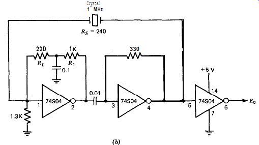
Figure 11.3(b). TTL Two-Inverters (74304) circuit. Set RL z R,, (R, + RI)
E 1.2K-o.
The schematic of this series-resonant circuit at 1 MHz is shown in Fig. 11.4. This circuit's performance is below average. The LM319 is the fastest of the two voltage comparators (LM319 and LM339) currently available for operation from a single +5 VDC supply. The (+) input terminal is referenced to +2.5 VDC. R1C1 provides negative feedback at low frequencies to hold the comparator's DC output in the middle of its transition range in order to ensure oscillation at start-up.
Waveforms at the crystal are reasonable, but the crystal's load resistance RL of 510 R is higher than it should be at 1 MHz with respect to the crystal's internal series resistance of 240 R. This is due to the amplifier's high output impedance, which is too high for good operation at 1 MHz. If ...
Figure 11.3(c).
TTL Two-Inverters (74LSO4) circuit. Set R,z R,, (RL + R,) =7K 0.
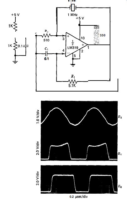
Figure 11.4. TTL voltage comparator (LM319) at 1 MHz. (LM319 Copyright 1981
National Semiconductor Corporation.)
... the crystal's load resistance EL is made lower than 510 a, the crystal drive waveform E, becomes even more distorted than is shown in Fig. 11.4. At 500 kHz and below, the crystal's internal series resistance R, and its load resistance RL are both higher, and the crystal loading and drive waveform problems improve considerably.
The comparator's input impedance is highly nonlinear. This would warp the crystal's sine wave output much more than is shown in Fig. 11.4 if it were not for the linearizing effect of the crystal's load resistor RL, which is effectively in parallel with the comparator's input impedance.
This nonlinear loading effect will show up more at lower frequencies, where the desired crystal load resistance RL is higher. Waveforms in Fig. 11.4 show about an 80-nsec time delay in the LM319 comparator, which limits it to frequencies below 500 kHz for good oscillator operation. But the nonlinear loading effects that occur at these lower frequencies mean that the LM319 will not work well as an oscillator at any frequency. An additional drawback is that the circuit continues to oscillate at a spurious frequency when the crystal is removed.
11.5. TTL RECEIVER--9615
The circuit of this oscillator at 1 MHz is shown in Fig. 11.5. The circuit gives above-average performance. Both receiver inputs are internally biased at + 1.9 VDC. R ,C r provides negative feedback at low frequencies to servo the output at pin 1 to + 1.9 VDC, approximately in the middle of the transition region, in order to ensure oscillation at start-up.
Waveforms at the crystal are very good. The frequency is not very sensitive to power supply or temperature changes. The crystal's load resistance RL is set equal to or somewhat less than the crystal's internal series resistance R,.
The circuit uses very few parts and will operate from 100 kHz to 2 MHz. There are two 9615 receivers in a DIP, and the second one makes a convenient isolating buffer for the oscillator.
11.6. TTL RECEIVER--8820
The schematic for this oscillator at 1 MHz is shown in Fig. 11.6. R, biases the negative (-) input terminal (pin 1) to approximately the same +2.5 VDC bias point as the positive (+) input terminal. R,C, applies negative feedback at low frequencies to hold DC output at the mid point of the transition region in order to ensure oscillation at startup.
Waveforms at the crystal are fairly good. The output impedance of the 8820 at pin 6 is too high to properly drive a 1-MHz crystal, and so the tops of the E, square wave curve downward as the crystal's sine wave of current flows back into its driving source at pin 6. Because of this, the crystal's load resistance, which consists of R L and the 8820's input resistance of 2.5K ohm in parallel, is not so low as desired. With RL = 1K ohm , the net crystal load is 715 ohm, which is about 3 times higher than the crystal's internal series resistance of 240 ohm. This reduces the circuit's short-term frequency stability.
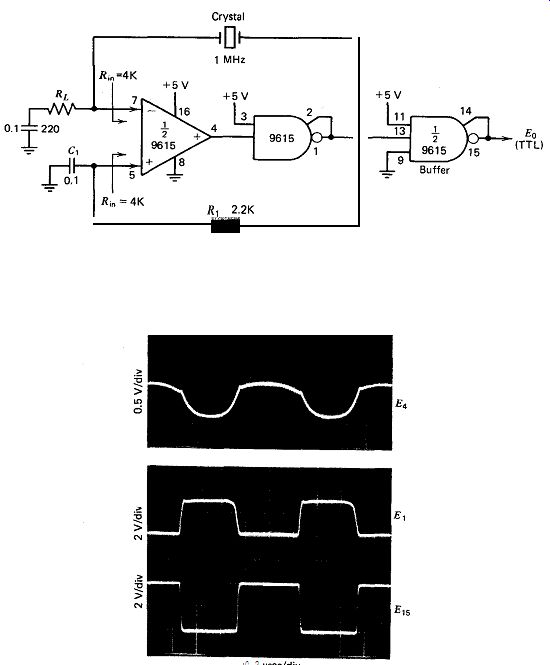
Figure 11.5. TTL receiver (9615) at 1 mHz. (9615 Courtesy Fairchild Camera
and Instrument Corporation.)
The waveform of the square wave driving the crystal would look better at frequencies of 500 kHz or lower, where the crystal's internal series resistance R, is higher. The waveforms show about a 70-nsec time delay in the 8820 line receiver.
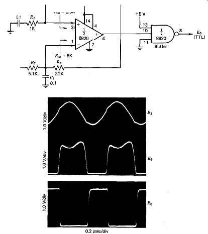
Figure 11.6. TTL receiver (8820) at 1 mHz. (8820 Copyright 1981 National Semiconductor
Corporation.)
11.7. ECL RECEIVER--10114
The schematic of this series-resonant oscillator at 1 MHz is shown in Fig. 11.7a and the circuit waveforms in Fig. 11.7b. This circuit has outstanding performance and works very nicely off a +5 VDC supply. Waveforms at the crystal are very good, equal to the best of any circuit tested. The frequency changes very little when power supply voltage or temperature is changed. The low ECL drive voltage keeps crystal dissipation low.
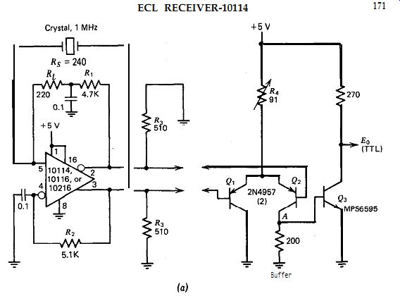
Figure 11.7(a). Series-resonant circuit in ECL at 1 MHz. Set R1 = R,. (10114,
10116, 10216 Courtesy Motorola, Inc.)
And the low ECL drive resistance means the crystal can have a low load resistance R_L, which gives very good short-term frequency stability.
The ECL receiver format is well-adapted to high-frequency oscillator circuits. At high frequencies, crystals are low impedance devices, and ECL circuits can drive low impedance loads down to 50 ohm easily. Input resistances of ECL circuits are high, and they are also linear over the ECL voltage range. As shown in Fig. 11.7b, the crystal's square wave drive waveform at pin 3 has a definite slope during transitions between binary states, indicating the ECL unit is operating as a linear amplifier during the transition interval.
The 10114, 10116, and 10216 are similar in that they have the same pin connections and are directly interchangeable in the circuit in Fig. 11.7. They differ slightly in speed and internal construction. All three have the required push-pull inputs and outputs needed for an ECL oscillator. The 10216 has the widest bandwidth and should be used at the highest frequencies (4-20 MHz). The 10116 has medium bandwidth and should be used at medium frequencies (1-6 MHz). The 10114 has the least bandwidth and should be used at lower frequencies (500 kHz-4 MHz).
Figure
11.7(b). Waveforms for series-resonant-ECL circuit in Fig. 11.7a.
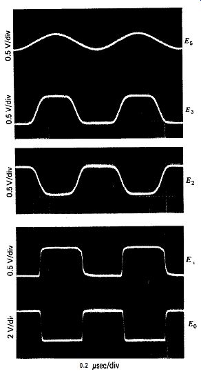
Figure 11.7c shows the circuit at 20 MHz. The crystal's internal series resistance R, is 7 CR; the crystal's load resistance RL is 10 R.
At 20 MHz, the ECL receiver has to be able to drive a 17-R load (R, + RL = 17 a), a very low value. The receiver's output resistance is controlled by the ECL emitter's output current, which is, in turn, controlled by the emitter's pulldown resistor R3. R3 = 510 R works well at 1 MHz, but it has to decrease to 100 R at 20 MHz to get the ECL output resistance down low enough to provide a reasonable drive waveform to the crystal.
There are three ECL receivers in one DIP. One of the two unused ones could be used as a no-cost buffer between the oscillator and the two-transistor buffer, but the circuit will oscillate spuriously when the crystal is removed. Because of this, the ECL receivers are not used as buffers.
The buffer circuit is specifically designed to minimize capacitive loading (the Miller effect) from the buffer onto the oscillator, which can ...
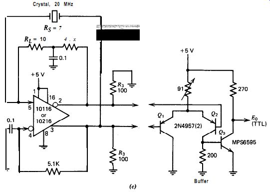
Figure 11.7(c). Series-resonant circuit in ECL at 20 MHz. Set R, = R,. (10116,
10216 Courtesy Motorola, Inc.)
... change the oscillation frequency. Part of the buffer design shown in Fig. 11.7 is taken from Blood [20]. To minimize the Miller capacitance effect, Q1 is operated without a collector load resistor, and the voltage swing at the collector of Q2 is limited to 0.7 V peak by the base-emitter junction of Qs. The square wave on/off ratio at the output of Q3 depends on the gain of Qs, which varies from one transistor to the next. The on/off ratio at the output also depends on R,. Making R4 adjustable provides an adjustment of the on/off ratio at the output if it is needed.
C. PIERCE 11.8. CMOS INVERTEIL -- 74C04
The circuit of this Pierce-IC oscillator at 1 MHz is shown in Fig. 11.8.
The output resistance R. of the first inverter is used as the integrating resistor for the R,,C, phase-lag network. Small values of C, and C, are used in order to minimize the gain reduction they introduce. One result of this is that the crystal oscillates a little higher above its series-resonant frequency. RI provides negative DC feedback around the inverter in order to put it in the linear region so that oscillation will start when ...
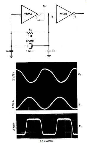
Figure 11.8. Pierce in CMOS (74C04). (74C04 Copyright 1981 National Semiconductor
Corporation.) At a frequency of 1 MHz, C, and pF; at a frequency of 2 MHz,
C, and C, = 330 pF. For Solid State Scientific's 4000A/B series only, at a
frequency of 5 MHz, C, = 330 pF and C2 = 100 pF.
... power is applied. The second inverter squares up the output waveform and also acts as an isolation buffer.
This CMOS circuit works reasonably well at frequencies up to 1 MHz.
Above 1 MHz, variations among manufacturers show up, and only certain brands will work satisfactorily. National Semiconductor's 74C series will work up to 2 MHz, and Solid State Scientific's 4000A/B series will work up to 5 MHz. Capacitance values of C, and C2 at 1, 2, and 5 MHz are listed in Fig. 11.8. Above 2 MHz, the crystal's dissipation should be checked, so that its dissipation limit is not exceeded.
11.9. TTL VOLTAGE COMPARATOR--LM319
The schematic of this Pierce-IC at 1 MHz is shown in Fig. 11.9. The LM319 is a voltage comparator with a relatively large 60-nsec internal time delay, which limits its upper oscillation frequency to about 2 MHz.
There are faster comparators available, but they require rt15 V power rather than only +5 V. The LM319's high input impedance allows it to operate at frequencies down to 10 kHz. Its input impedance is quite nonlinear, however, which will distort the crystal's output waveform at lower frequencies. R, and R3 provide a DC feedback to ensure that the comparator is in its linear conducting region and will start oscillating when power is applied.
The LM319 performs well as a Pierce oscillator. The 50-ohm reactive impedance of the 3300-pF capacitor C, (at 1 MHz) swamps out the LM319's nonlinear input impedance, and the voltage waveforms at the crystal are reasonably good. The on/off ratio at the output can be adjusted closer to 50/50 than is shown in the waveform photograph by adjusting the ratio of the biasing resistors R4 and R5. The circuit does have the disadvantage that it oscillates spuriously with the crystal out of the circuit. There are two LM319 comparators in a DIP, and for convenience, the second one is used as an isolation amplifier.
11.10. ECL RECEIVER--10114
A schematic of this Pierce-IC at 1 MHz is shown in Fig. 11.10 and its waveforms in Fig. 11.10b. Three ECL receiver stages are cascaded to provide the high gain required by the Pierce circuit. The circuit works well at 1 MHz with the 10114, but not with the 10116. R2 and R3 provide DC feedback around the receivers to bias them into the linear operating region, so that the circuit will start oscillating when power is applied.
Frequency stability with both power supply and temperature changes is very good; crystal waveforms are also reasonably good. One drawback to the circuit is the fairly large number of discrete parts required. The buffer circuit converts the oscillator's ECL output to a TTL format. The buffer is designed to minimize capacitive loading effects on the oscillator. circuit. The design of the buffer is discussed in more detail in Section 11.7.
Figure 11.9. Pierce in TTL (LM319) at 1 MHz. (LM319 Copyright 1981 National
Semiconductor Corporation.)
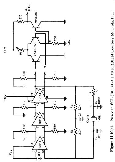
Figure 11.10
Figure 11.10(b). Waveforms for Pierce-ECL circuit in Fig. 11.10.
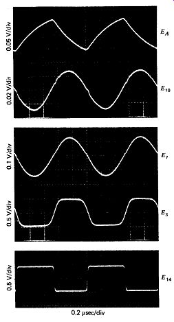
Figure 11.10 shows the same circuit at 20 MHz. Either the 10116 or the 10216
can be used at this frequency, but not the 10114, which does not have enough
gain at 20 MHz for the circuit to oscillate. This circuit gives good performance
and has good waveforms at the crystal. Note that the output resistance of the
ECL stage that drives the crystal has been lowered by decreasing emitter-pulldown
resistors R4 to 200 R, so it can drive the low resistance crystal load at 20
MHz. The frequency sensitivity of the 10116 to power supply changes is only
half that of the 10216.
The 10116 oscillates spuriously when the crystal is removed from the circuit, but the 10216 does not. For best short-term frequency stability, C, should be four times larger than the 470 pF shown in Fig. 11.10c, but the circuit does not have enough gain to permit the additional gain loss involved in doing this. Circuit layout is important in this circuit to pre vent spurious oscillation.
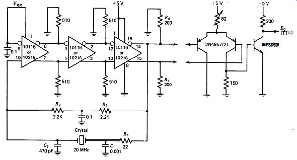
Figure 11.10(c). Pierce in ECL (10216) at 20 MHz. (10116, 10216 Courtesy Motorola,
Inc.)
INTEGRATED CIRCUIT OSCILLATORS D. MEACHAM
11.11. MEACHAM--10114
As an IC oscillator, the Meacham circuit's needs for both positive (+) and negative (-) bridge drive signals effectively limits it to ECL. An ECL receiver has both (+) and (-) inputs and outputs and provides an opportunity to try Meacham's full-bridge rather than only the half-bridge circuit. A schematic of Meacham's full-bridge circuit at 10 MHz is shown in Fig. 11.11; it is a complex circuit with good performance. Figure 11.11b shows voltage waveforms at several points in the circuit in Fig. 11.11~.
The 10114 works well in this circuit, but not the 10116 or the 10216.
The amplifier uses two ECL stages, giving a gain of 18X from point A to pin 14. If three ECL stages are used, the amplifier becomes unstable and oscillates parasitically at 60 MHz. Emitter-pulldown resistors at the ECL amplifier's output are set to give maximum emitter current, which gives the lowest possible output resistance. This is needed to drive the crystal's low internal series resistance R, of 5 ohm.
C, and C, permit negative feedback at DC, stabilizing the bias point and ensuring that oscillation will start when power is applied. C, balances out the crystal's shunt terminal capacitance Co, which helps minimize parasitic oscillation.
The bridge excitation is a square wave. The resonant L,C, tank selects the fundamental sine wave from the bridge output, ignores the harmonics, and reduces the response at frequencies away from resonance.
R, reduces the L,C, phase shift from 90 degr. down to 0 degr. at frequencies far away from resonance. R3 isolates L,C, from the crystal. The waveform clean-up by the L,C, tank can be seen inE2 (waveform at pin 2), which is proportional to the differential input signal between pins 4 and 5 in Fig. 11.11. The peculiar looking waveform E, out of the bridge at point A is normal and occurs when a square wave with sloping sides (through bridge arm R,) is subtracted from a sine wave (through the crystal arm).
The minimum theoretical value for R2 is equal to the crystal's internal series resistance R, of 5 R. The minimum practical value for R2 measures 8.2 R, which gives a practical to theoretical minimum ratio of 8.215 or 1.6 for RP.
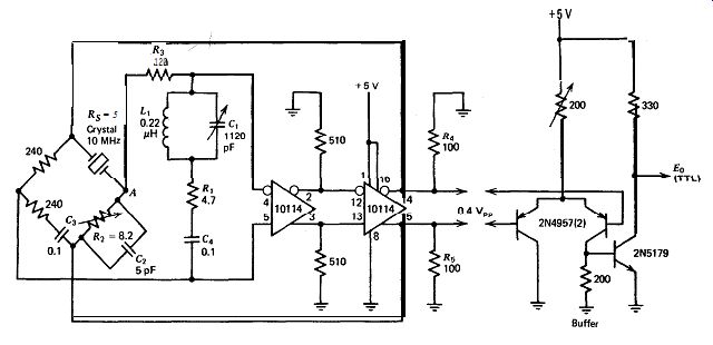
Figure 11.11(a). Meacham at 10 MHz. (10114 Courtesy Motorola, Inc.)
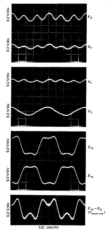
Figure 11.11(b). Waveforms for Meacham circuit in Fig. 11.11~1.
Meacham's full-bridge circuit can be changed into the modified Meacham half-bridge circuit shown in Fig. 11.1 1c. The isolation resistor R, is increased to 240 ohm to compensate for the drop in bridge source resistance when the two 240-a bridge arms are removed. The performance of the half-bridge circuit is just as good as that of the full-bridge ...
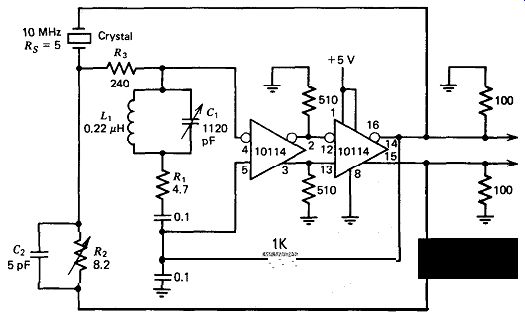
Figure 11.11(c). Modified Meacham at 10 MHz. (10114 Courtesy Motorola, Inc.)
... circuit, as far as could be measured. The minimum practical value for R2 in the half-bridge circuit is also 8.2 R, which gives the same ratio of 8.215 or 1.6 for R,. The full-bridge circuit does cancel out source resistance variations in the bridge drive, so its frequency stability is potentially better than that of the half-bridge circuit. The short-term stability of both circuits measured 0.1 ppm, at the limit of available measuring equipment. The full-bridge circuit is preferred to the half-bridge; the only ad vantage of the half-bridge circuit is that it uses one less resistor than the full-bridge circuit.
E. SPECIAL OSCILLATOR ICs
11.12. CMOS 7209
The schematic of this Pierce-IC oscillator at 10 MHz is shown in Fig. 11.12. The 7209 uses a single CMOS inverter in the oscillator circuit and has an internal feedback resistor around the inverter to bias the input into its linear conducting region and ensure oscillator start-up when power is applied. The advantage of the 7209 is that it will oscillate at frequencies up to 10 MHz, while an ordinary CMOS inverter quits at 2-5 MHz in the Pierce circuit (see Section 11.8). The oscillator and its fundamental frequency output will operate at frequencies down to at least 4 kHz.
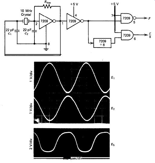
Figure 11.12. 7209 at 10 MHz. (7209 Reproduced by permission of Intersil,
Inc. from Data Sheet ICM 7209 CMOS Clock Generator. Copyright 1979 Intersil,
Inc. All rights reserved.)
The 7209 provides a second output frequency at '/a the crystal frequency. This divide-by-eight output uses dynamic divider circuitry, which will operate at 2 MHz (crystal frequency) with a 5 V supply voltage. The divide-by-eight circuit will work at crystal frequencies lower than 2 MHz by reducing the supply voltage below 5V. When the crystal is removed from the circuit, the fundamental frequency output stops (as it should), but the dynamic divide-by-eight frequency output at pin 6 continues to free run at a spurious frequency.
The 7209 gives reasonably good performance at both 1 and 10 MHz.
At 1 MHz, it operates over a wide range of supply voltage and tempera ture. At 10 MHz, the supply voltage must be greater than +4 V, and the temperature rise above ambient must be somewhat less than what is permissible at 1 MHz, or the output voltage swing at pin 5 will drop to zero.
In a Pierce circuit, the values of the two capacitors C, and C, should be changed when the frequency is changed. At 1 MHz, both C, and C, in Fig. 11.12 should be 100 pF. And at 100 kHz, both C, and C, should be 470 pF.
The 10-MHz waveform photographs in Fig. 11.12 show that voltage across the crystal is 2.4 Vrms, while Fig. 2.5 shows that maximum crystal voltage at series resonance is 0.3 Vrms at 10 MHz. Is the crystal's 2-mW dissipation limit being exceeded? The answer is no, because the crystal is operating inductively, way above series resonance. The current through the crystal can be determined from the voltage drop across the crystal load. Figure 11.12 shows 1.4 Vrms across a tptal capacitive load of about 32 pF (22 pF plus 5 pF stray plus 5-pF amplifier input capacitance). At 10 MHz, 32 pF has an impedance of 520 R, which gives a crystal current of 1.4/520 = 2.7 mA rms. Figure 2.3 shows a maximum crystal series resistance R, of 25 n at 10 MHz. Calculating the crystal's power dissipation from Z'R, gives 0.18 mW, which is less than the crystal's 2-mW dissipation limit.
11.13. TTL 74LS321
The 74LS321 uses a variation of the common base amplifier circuit, and a brief schematic at 1 MHz is shown in Fig. 11.13. The 74LS321 operates over a frequency range of l-20 MHz and is the oscillator section of the 74LS362. The 74LS320 is identical to the 74LS321 except that the divide-by-two and the divide-by-four frequency outputs have been deleted in the 74LS320.
The source and load resistances seen by the crystal looking back into the circuit at pins 14 and 15 both measure 40 Q giving the crystal an external load resistance of 80 R. The inductor L1, together with the collector resistor R,, provides a phase-lead network in the oscillator loop.
The inductance value to be used for L1 varies with frequency, and the circuit will not oscillate unless the proper inductance value is used.
Table 11.1 lists inductance values recommended by the manufacturer at various frequencies. From a design point of view, it is not necessary to use an inductor to make a common base amplifier circuit operate as a fundamental oscillator over the l-20-MHz frequency range. The inductor is apparently carried over from the 74LS362 design, where it was needed to provide an LC tank for harmonic operation at 48 MHz.
Figure 11.13. 74LS321 at 1 MHz. (74LS.321 Courtesy Texas Instruments Incorporated.)
TTL SP705B

TABLE 11.1 Inductance to Be Used in the 74LS321 Circuit at Various Frequencies
This circuit does not perform very well; the voltage waveform driving the crystal is poor. At 1 MHz, the frequency is reasonably stable and changes only 4 ppm when the power supply voltage is changed from 4 to 6 V. But at 20 MHz, the frequency drifts 1 ppm short-term-wise and changes IO2 ppm when the power supply voltage is changed from 4 to 6 V.
11.14. TTL SP705B
A schematic of this circuit at 1 MHz is shown in Fig. 11.14. The SP705B uses the common base amplifier circuit and is designed for frequencies up to 10 MHz. No minimum frequency is specified by the manufacturer, but the crystal's internal series resistance R, is specified at 300 ohm maximum, which corresponds to a minimum frequency of about 1 MHz.
Looking back into the circuit at pin 6, the source resistance R, driving the crystal is 110 R, and looking back into the circuit at pin 5, the crystal's load resistance RL is 32 a. This gives a total resistive load on the crystal of 142 a. This is a reasonable load value at 1 MHz, where the crystal's internal series resistance R, is 240 a, and gives fairly good in circuit Q and short-term frequency stability at 1 MHz. But 142 R is too high a load resistance at 10 MHz, where the crystal's internal series resistance is about 15 a. This high load resistance reduces both the crystal's in-circuit Q and the short-term frequency stability at higher frequencies.
----------
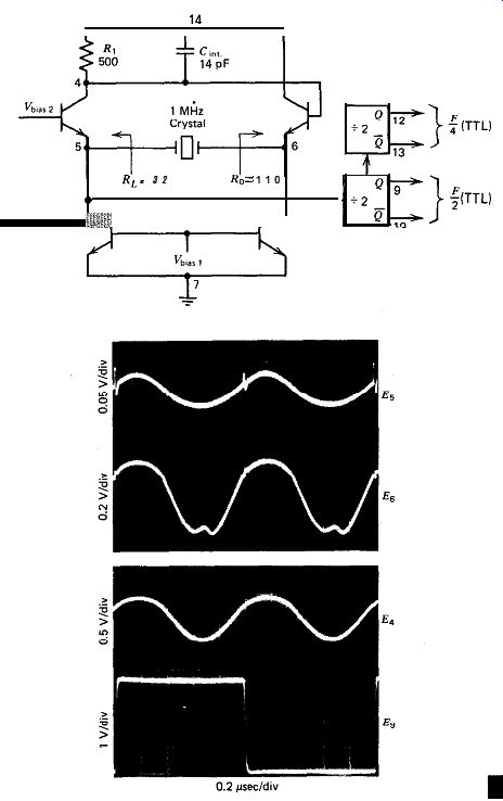
SP705B at 1 MHz. (SP705B Courtesy Plessey Semiconductors.)
At 1 MHz, it takes the circuit about 1 second to start oscillating, but at 10 MHz, it starts immediately. Only the half-frequency and quarter frequency outputs have a TTL format. The crystal's fundamental frequency is available at pin 6, but it is a low voltage signal (0.6 Vp-p) and will not drive TTL circuitry directly.
The circuit's performance is fair at 1 MHz but poor at 10 MHz.
Waveforms at the crystal are poor; the driving waveform is distorted, and the output waveform shows a pair of switching spikes riding on top of the waveform. At 1 MHz, the oscillation frequency is relatively insensitive to temperature and power supply voltage changes, But at 10 MHz, the frequency shifts 47 ppm when the power supply voltage changes from 4 to 6V.
11.15. ECL 12061
A schematic of this IC oscillator is shown in Fig. 11.15. This oscillator uses a variation of the common base amplifier circuit and incorporates an AGC (automatic gain control) loop to keep oscillation amplitude at a low level and minimize power dissipation in the crystal. The oscillator has three outputs: sine wave, ECL, and TTL and comes in two frequency ranges: the 12060 for a 100 kHz-2 MHz operation and the 12061 for a 2-20 MHz operation. In the 12060, the source and load resistances seen by the crystal looking back into pins 5 and 6 are both 2.7K Q giving a total crystal load resistance of 5.4K R. In the 12061, the source and load resistances looking back into pins 5 and 6 are both 130 R, giving a total crystal load resistance of 260 R. A 0.1-PF bypass capacitor is required directly across the oscillator section's power pins from pin 1 to pin 8 to minimize noise coupling into the oscillator. If the TTL output section is used, a second 0.1-p.F capacitor is required directly across its power pins from pin 9 to pin 11 to minimize noise coupling of the TTL switching transients into the oscillator section.
Unfortunately, neither the 12060 nor the 12061 work very well, particularly at the high-frequency ends of their range. Crystal waveforms are poor; the ~-MHZ waveforms shown in Fig. 11.15 for the 12061 are typical of either IC at any frequency. The 12060 is reasonably insensitive to power supply and temperature changes at 100 kHz. But at its upper frequency limit of 2 MHz, the frequency is unstable with temperature and shifts 150-180 ppm when heated or cooled above or below ambient.
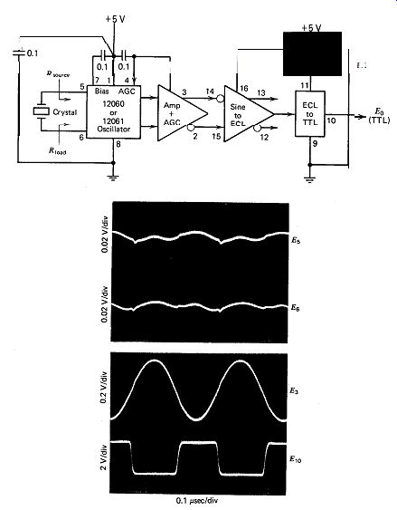
Figure 11.15. 12060, 12061 circuit. Waveforms are for the 12061 (12060, 12061
Courtesy Motorola, Inc.) at 2 MHz.
The 12061 works reasonably well at its low frequency limit of 2 MHz, but at its upper frequency limit of 20 MHz, there is a relatively large Id-ppm frequency shift when the power supply voltage is changed from 4 to 6 V and a large 28-ppm frequency shift when heated above ambient.
The basic difficulty seems to be that IC source and load resistances seen by the crystal are scaled for operation at the low end of each frequency range and are too large to operate well at the high end.
11.16. LINEAR LM375
A schematic of this series-resonant circuit at 500 kHz is shown in Fig. 11.16. The LM375 contains two buffer amplifiers and provides both sine wave and TTL outputs. A sine wave rather than a square wave can be obtained from the first buffer by interchanging its input leads and disconnecting the TTL driver. The LM375 oscillator section contains a very wideband amplifier, with a relatively high output resistance at pin 5. Because of the amplifier's wide bandwidth, it is necessary to add capacitor C, across the oscillator's input at the lower frequencies (500 kHz), as shown in Fig. 11.16a, in order to avoid extra noise switchings when the oscillator's waveform switches polarity.
With a resistive load R, on the oscillator, the highest oscillation frequency is limited to about 500 kHz because of loading effects on the oscillator's high output resistance. Above 500 kHz, the amplifier's square wave output gets too distorted to drive a low resistance crystal.
The LM375 can be used at frequencies up to 10 MHz if a tuned LC tank instead of the resistor R, is used for the oscillator load. Figure 11.16b shows a circuit for 10 MHz operation. The crystal is tapped down on the LC tank in order to raise the crystal's low internal resistance R, to a much higher value, as seen by the amplifier's output at pin 5.
Tapping down the crystal on the LC tank has a considerable effect on the circuit, and this is discussed in detail in Sections 5.13 and 7.6.
The oscillator section of the LM375 will work at up to 60 MHz, but the buffer and TTL driver circuits will not operate properly above 10 MHz.
From a general design viewpoint, it is not necessary to use an LC tank for fundamental operation at 10 MHz, but it is needed here because the oscillator's high output resistance needs a high load impedance to work into.
The oscillator performs well with a resistive oscillator load at and below 500 kHz. Crystal waveforms are good, and the oscillation frequency is relatively independent of power supply and temperature changes.
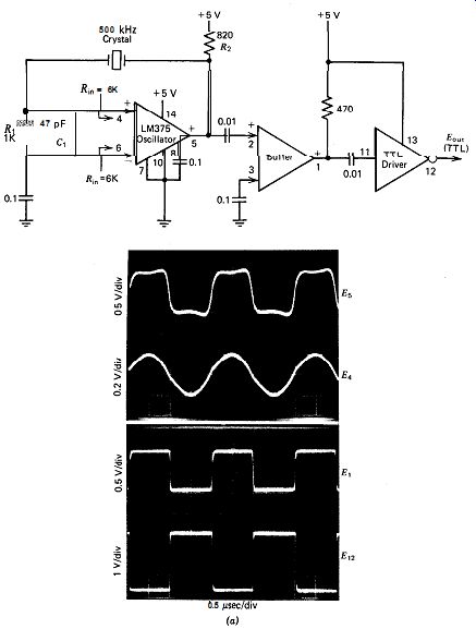
Figure 11.16(a). LM375 at 500 kHz. (LM375 Copyright 1981 National Semiconductor
Corporation.)
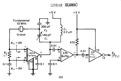
Figure 11.16(b). LM375 at 10 MHz. (LM375 Copyright 1981 National
Semi conductor Corporation.)
The oscillator gives only a fair performance with a resonant LC tank for the oscillator load. The crystal's load resistance RL at 10 MHz should be about 10 R or less but could not be reduced below 33 ohm without starting parasitic oscillations. In addition, the circuit oscillates spuriously when the crystal is removed from the circuit. The LM375 has been discontinued by the manufacturer.
11.17. LINEAR SL680C
A schematic of this emitter coupled circuit at 2 MHz is shown in Fig. 11.17a, and its waveforms are shown in Fig. 11.17b. The SL680C has an AGC loop to keep the crystal's power dissipation low; it has only a sine wave output, at pin 6. The emitter follower output at pin 7 should not be used, since any external noise picked up here couples directly onto the crystal, and any loading effects will reduce loop gain and may prevent the circuit from oscillating.
The power supply voltage of the SL680C is rated at +6 to +10 VDC, but it will operate at +5 V if a sine wave output with its negative peak flattened off is acceptable. Waveforms in Fig. 11.17b are for a +6 V rather than +5 V supply, in order to show the sine wave output at pin 6 when the IC is operated within its rated power supply range.
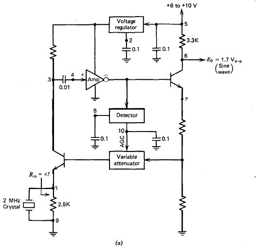
Figure 11.17(a). SL680C at 2 MHz. (SL680C Courtesy Plessey Semiconductors.)
The load resistance seen by the crystal looking into pin 1 is 45 a. The loop gain of the emitter coupled circuit varies inversely with the crystal's internal series resistance R,, which means that loop gain decreases as frequency decreases. The SL680C oscillated properly at frequencies of 2-20 MHz but would not oscillate at 1 MHz or lower. It would not operate harmonically much above 20 MHz even when a parallel tuned LC circuit (AC coupled) was added from pin 4 to ground in Fig. 11.17~.
The circuit gives good performance at 2 MHz and fair performance at 20 MHz. Operating the circuit at +5 VDC rather than at +6 V makes little difference at 2 MHz other than the flattened negative peak on the sine wave output. At 20 MHz and +5 V, frequency is fairly sensitive to the power supply voltage, changing 35 ppm when the power supply voltage is dropped from +6 V to +5 VDC. The frequency shift is much less within the SL680C's rated supply range, changing only 3 ppm when the power supply voltage is changed from +6 to +8 V. Also, at 20 MHz, the frequency changes quite a bit (12 ppm) when heated above ambient regardless of whether the power supply voltage is +5 V or +8 V.
Figure 11.17(b). Waveforms for SL680C circuit in Fig. 11.17~.
F. VHF HARMONIC
11.18. ECL RECEIVER-10216 (100 MHz)
This is a VHF harmonic oscillator that uses an ECL IC for its amplifier. It is a series-resonant circuit oscillating at 100 MHz, with a capacitive tap on the LC tank; the schematic is shown in Fig. 11.18. The circuit is a variation of Butler's emitter follower circuit in Fig. 5.31, with the emitter follower having a gain of 1.5-6X instead of just 1X. For frequency stability, L, must have an air core, while L, is not very critical and can have an iron core. R, has a big effect on circuit operation; if R, is too high, L,C, tunes so strongly that it takes control over the oscillation frequency away from the crystal. If R, is too low, it broadens the bandwidth of the L,C, tank so much that the tank loses its primary function of selecting which harmonic the crystal is to oscillate at. If R, is made even smaller, loop gain becomes less than 1X, and the circuit will not oscillate at all.
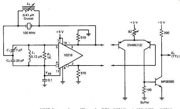
Figure 11.18. VHF harmonic oscillator in ECL (10216) at 100 MHz. (10216 Courtesy
Motorola, Inc.) This circuit works very well. Its short-term frequency stability
is very good, and its sensitivity to power supply changes is low and reasonably
low to temperature changes. The circuit shows no parasitic oscillation effects.
The buffer is designed to minimize capacitive loading effects on the oscillator
circuit. The design of the buffer is discussed in more detail in Section 11.7.