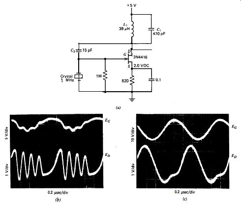
Figure 10.1. Miller-FET at (a) 1 MHz, (b) C, = 0, and (c) C1 = 470 pF.
| Home | Audio mag. | Stereo Review mag. | High Fidelity mag. | AE/AA mag. |
This section contains performance test data on the discrete transistor oscillator circuits described in Section 5. It is divided into three parts: The first describes the circuit selection and testing philosophy used; the second part describes individual fundamental oscillator circuits one by one; and the third describes individual harmonic oscillator circuits.
A. CIRCUIT SELECTION AND TESTING
The basic approach in selecting discrete transistor circuits was first to try all basic circuit types, then build a test circuit of each type to determine its strong and weak points. A total of 22 fundamental and 12 harmonic discrete transistor circuits were evaluated in this way. Where practical, the fundamental circuits were all tested at the same frequency of 1 MHz for comparison purposes, and the more important ones were also tested at the frequency extremes of 4 kHz and 20 MHz.
The harmonic circuits were tested at three frequencies: 20, 50, and 100 MHz. Except for special cases, 20 MHz is the lowest frequency at which a harmonic circuit would be used, and 100 MHz is near the upper 200-MHz harmonic frequency limit. 50 MHz was picked as near the middle of the harmonic frequency band.
After selection, each test circuit was individually optimized for best component values, bias, waveforms, and so forth. Because the transistors used have a strong effect on circuit performance, considerable time was spent selecting the right ones for each circuit. Many discrete transistor circuits are not compatible with digital logic, so level shifters or buffers were added to some of them to make them TTL compatible.
Photographs were taken of oscillator waveforms at various points in the circuits. The waveform photos of each circuit have been synchronized to a common point in time and vertically aligned together on the printed page to permit vertical phase comparisons between various parts of each circuit. To facilitate comparing the circuits with one other, the same crystals were used in all circuits, moving them from circuit to circuit as needed. The crystal most used is a 1-MHz crystal. It is an AT cut with an internal series resistance of 240 K! and is solder sealed in a gas filled HC-6 metal can.
The circuits were tested for frequency sensitivity to supply voltage and temperature variations. Sensitivity to supply voltage is checked by measuring the frequency shift when the power supply voltage is changed from +4 to +6 VDC. Since the object of the temperature testing was to measure temperature characteristics of the oscillator circuit itself and not the crystal, only the oscillator circuit was subjected to tempera ture changes, with the crystal left at room temperature. Temperature changes were obtained by the rather crude method of spraying the circuits (but not the crystal) with freon from an aerosol can for 10 seconds to cool the circuits, and blowing hot air on the circuits (but not on the crystal) with a heat gun for 20 seconds to heat the circuits. The tempera ture sensitivity numbers given in Tables 12.1, 12.2, and 12.3 are the changes in oscillator frequency when the circuit was heated or cooled in this fashion. The intention was to get a rough rather than accurate measure of the circuits' sensitivity to these effects.
The short-term frequency stability of some of the oscillator circuits was checked by measuring the frequency with a frequency counter and looking at the variation in frequency over a short 20-40 second time interval. Measured this way, short-term stability contains errors due to the + 1 count accuracy of the counter and inherent short-term frequency variations in the counter's internal oscillator. The intent, again, was to get a rough rather than accurate measure of the short-term stability of the different circuits.
Because temperature and short-term stability measurements were not very accurate, no attention should be paid to small differences in these numbers among circuits. Only a reasonably large difference has any significance.
No long-term frequency stability measurements were made on any oscillator circuits. There are several reasons for this. First, the stability needs of most digital circuitry can be satisfied with much less than the maximum stability obtainable from a crystal oscillator. Second, to be meaningful, any long-term stability measurements would have to be made over a protracted period of time. And third, even if such data were obtained, it would be difficult to sort out what was due to the circuit from what was due to the crystal.
B. FUNDAMENTAL CIRCUITS
10.1. MILLER-FET
The schematic of this oscillator at 1 MHz is shown in Fig. 10.1. The crystal operates as a shunt element in this circuit and requires a high load resistance to operate properly. A FET has a high input resistance and makes an ideal amplifier here. The parallel L,C, network is not at resonance and must have a net inductive impedance for oscillation to occur. Although C, is not necessary for oscillation to occur, the photo graphs in Figs. 10.1b and c show how much C, cleans up the waveform across L,. With C, = 470 pF, the waveform across the crystal improves to a very nice sine wave and increases considerably in amplitude. The oscillation frequency is very sensitive to C, and the drain-to-gate capacitance in parallel with C,. Because the effective value of C, is C, multi plied by the amplifier gain (the Miller effect), the frequency changes significantly when the FET is changed or when the stage gain changes with power supply or temperature changes. Because of this, the Miller circuit is not a very stable oscillator.
10.2. MILLER-TRANSISTOR
The schematic of this oscillator at 1 MHz is shown in Fig. 10.2. The purpose of this circuit is to show the heavy crystal loading that occurs if a bipolar transistor is used for the amplifier instead of a FET. The parallel L,C, network must have a net inductive impedance for oscillation to occur. Although C, is not necessary for oscillation to occur, waveform photographs in Figs. 10.2b and c show how much C, cleans up waveforms across both L, and the crystal. The crystal waveform in Fig. 10.2 is still very poor even with C, = 470 pF and shows that using a bipolar transistor rather than a FET gives a much poorer oscillator.
The oscillation frequency is very sensitive to C, and the transistor's
Figure 10.1. Miller-FET at (a) 1 MHz, (b) C, = 0, and (c) C1 = 470 pF.
collector-to-base capacitance in parallel with C,. Because the effective value of C, is C, multiplied by the amplifier gain (Miller effect), frequency changes significantly when the transistor is changed or when the amplifier gain changes with power supply or temperature changes. Be cause of this, the Miller circuit is not a stable oscillator.
10.3. COLPITTS-PET
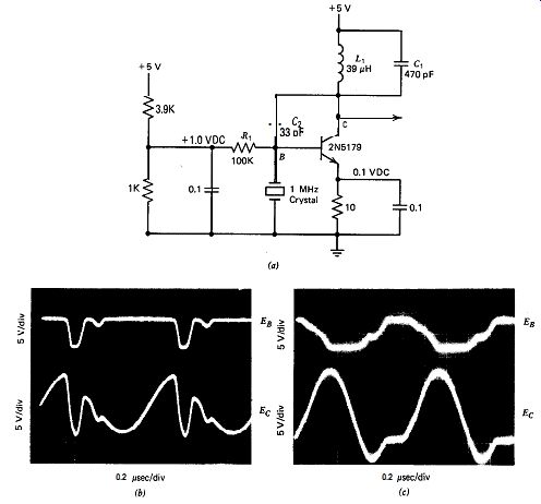
Figure 10.2. Miller-transistor at (a) 1 MHz, (b) C, = 0, and (c) C, = 470
pF.
A schematic of this circuit at 1 MHz is shown in Fig. 10.3~. The Colpitts is a parallel resonant circuit and requires a high shunt-load impedance on the crystal. A FET amplifier, with its high input impedance, is a good selection for the Colpitts oscillator. The voltage swing on the crystal is rather large, from +6 to -6 VDC. The waveform at the FET's source shows three operating modes over a cycle: conduction on a rising wave front, saturation limiting at the positive peak, and FET cutoff and RC exponential decay on a falling wavefront. The circuit has a good short-term stability of 2 0.1 ppm.
When the frequency is changed, the time constant R,C, must be changed. In the FET version, it is convenient to leave R, fixed (to hold. the drain current constant) and vary C,.
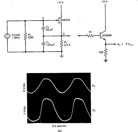
Figure 10.3 . Colpitts-FET at 1 MHz. R2 must be > 1 Ma for no loading
effects and > 22K R for oscillation to occur.
What happens when the resistor R, is replaced with an inductor? Figure 10.3b shows the same circuit with the 2.4K n emitter resistor R, replaced with a 550 qH inductor. The inductor's 3000-ohm reactance at 1 MHz is a little higher than the 2400 n of resistor R,, but it is close enough. Note the much larger waveform amplitudes in Fig. 10.3b when the inductor is used, so much so that the FET's gate goes above +5 VDC and acts as a diode clamp through the FET's drain to the +5 V power supply * The circuit in Fig. 10.3b is more important as a harmonic oscillator than as a fundamental one, but it is included here for waveform comparison with Fig. 10.3~. The larger voltage swing across the crystal shows that the in-circuit Q is much higher with the inductor L, rather than the resistor R, in the circuit.
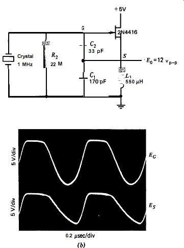
Figure 10.3(b). Colpitts-FET at 1 MHz, using an inductor L1 instead of resistor
R, in Fig. 10.3~. L,C, is not tuned to resonance.
A schematic for operation at 4 kHz is shown in Fig. 10.3. Note the very high shunt resistance required across the crystal to operate at 4 kHz.
A FET is the obvious choice for the amplifier in this circuit because of its high input resistance.
A schematic for operation at 10 MHz is shown in Fig. 10.3d. At these higher frequencies, the J309 FET works better than the 2N4416, be cause it has twice the transconductance of the 2N4416 and half the output resistance. The output resistance must be low to drive the low impedance of C, at high frequencies. The 5309 requires twice the drain current, so R, is cut in half to provide this. C, is then doubled to keep the R,C, time constant the same.
10 MHz is about the upper limit for a FET-Colpitts circuit. Above 10 MHz, a bipolar transistor makes a better amplifier choice. The output resistance of a transistor emitter follower is 5 to 10 times lower than that of a FET source follower, which makes it much easier for the transistor to drive the lower circuit impedance of a high-frequency oscillator circuit.
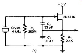
Figure 10.3(c). Colpitts-FET at 4 kHz. R2 must be 2 220 MR for no loading
effects and 2 5 M0 for oscillation to occur.
And the low crystal impedance at these higher frequencies makes the medium input resistance of a transistor amplifier more acceptable as a load for the crystal.
10.4. COLPITTS-TRANSISTOR
A schematic of this circuit at 1 MHz is shown in Fig. 10.4~. The voltage swing across the crystal is rather large, from +5 to -1 VDC. The waveform at the transistor's emitter shows three operating modes over a cycle: normal transistor operation over a short interval near the end of the rising crystal waveform, transistor saturation at the positive signal peak, and transistor shut-off and a long RC exponential decay with a falling crystal waveform. The circuit has a good short-term stability of * 0.1 ppm.
To change frequency, the time constant R,C, must be changed. In the transistor version of the Colpitts, it is convenient to change R, and leave C, fixed. This increases the transistor's input resistance as the frequency goes lower, where the crystal's load resistance must be higher. It also
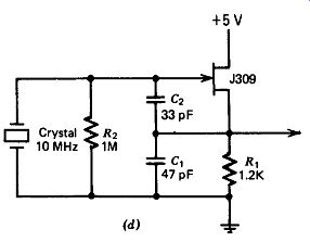
Figure 10.3(d). Colpitts-FET at 10 MHz.. R, must be 2 100K-o for no loading
effects and 2 3.3K-o for oscillation to occur.
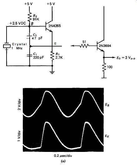
Figure 10.4(a). Colpitts-transistor at 1 MHz. Crystal shunt resistance must
be 2 1 MR for no loading effects and 2 22K ohm for oscillation to occur.
... helps to use a high-gain transistor to get the highest possible input resistance at the transistor's base input terminal and minimize crystal loading by the transistor.
What happens when the resistor R, is replaced with an inductor? Figure 10.4b shows the same circuit as Fig. 10.4 but with the 2.7K ohm emitter resistor R1 replaced with a 550qH inductance I,,. Its reactive impedance is 3.1K -ohm at 1 MHz, roughly near the 2.4K-o of R1. The bias resistor R, is increased to 470K 52 to compensate for removing the emitter resistor R,.
The waveforms show an increased Q, with signal voltages almost three times larger in amplitude and the peaks showing stronger clipping. This circuit is more important as a harmonic oscillator than as a fundamental one, but it is included here for waveform comparison with Fig. 10.4.
A schematic for operation at 200 kHz is shown in Fig. 10.4. 200 kHz
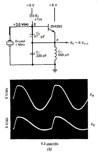
Figure 10.4(b). Colpitts-transistor at 1 MHz, using an inductor L1 for resistor
RI in Fig. 10.4~. L,C, is not tuned to resonance.
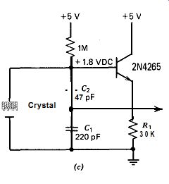
Figure 10.4(c). Colpitts-transistor at 200 kHz. Crystal shunt resistance must
be 2 470K R for no loading effects and 2 220K R for oscillation to occur.
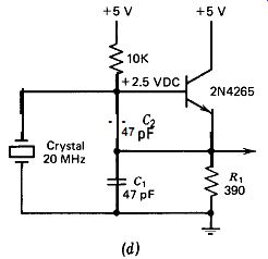
Figure 10.4(d). Colpitts-transistor at 20 MHz. Crystal shunt resistance must
be 2 22K R for no loading effects and 2 2.2K ohm for oscillation to occur.
... is about the lowest frequency at which a transistor-Colpitts circuit will work because of crystal loading effects. Below 1 MHz, oscillation amplitude is quite low because of crystal loading by the transistor. At frequencies below 1 MHz, a FET is a better choice than a transistor for the Colpitts circuit. A transistor-Colpitts circuit for operation at 20 MHz is shown in Fig. 10.4d.
10.5. LOW CAPACITANCE LOAD
A schematic of this circuit is shown in Fig. 10.5. The circuit shows good performance; its short-term stability is a good 0.1 ppm. One criticism is that the crystal driving waveform could be more symmetrical than it actually is. As can be seen from the waveforms, the FET input signal is so large that it effectively turns the FET on and off like a half-wave rectifier.
Increasing C, would help square up the crystal driving waveform. When the FET amplifier input saturates on the positive signal peaks, the only effect on the crystal is that capacitive divider impedance changes from 9.5 to 12 pF. Amplifier gain from point A to point C in Fig. 10.5~ is only 0.8X, and additional gain is provided by partial resonance of C, and C, in series with the crystal's internal inductance.
Measuring the crystal current by means of the voltage drop across the series capacitor C, introduces a 90 degr. phase lag. The RC networks R3C3 and Z&C, each introduce an additional 45 degr. phase lag, and the transistor inverts the signal, providing a total phase shift of 360 degr. around the amplifier loop.
Due to the low capacitance load effectively in series with the crystal, the oscillation frequency is about 300 ppm higher than it would be with a low impedance load. This is as expected and what normally occurs in an
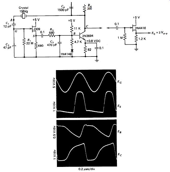
Figure 10.5(a). Low-capacitance load circuit at 1 MHz.
... oscillator circuit when a small frequency-trimming capacitance is put in series with the crystal.
Are the low capacitance divider and the high resistance of the FET amplifier input effective in reducing resistive load losses?
Figure 10.5. Equivalent crystal load for low-capacitance load circuit: (h)
crystal load circuit, (c) intermediate, and (d) equivalent load circuits.
The answer is yes. Figures 10.5b-d show the equivalent crystal load circuit. Converting the parallel RC network of C2 (47 pF) and R, (22 M-ohm) to its series equivalent gives 47 pF and 0.6 a. The 0.6 ohm is negligible. The largest resistive loss comes from the driving source resistance Rd. Since Z&C, is shorted to ground by the transistor every half cycle, the effective R4C4 impedance values are halved, or 3000 pF and 100 ohm average over the complete waveform cycle, as shown in Fig. 10.%. The final equivalent load on the crystal is 9.7 ohm in series with 14 pF, as shown in Fig. 10.5d.
The low 9.7-a series resistance is the major reason for the circuit's good short-term frequency stability of 0.1 ppm.
Converting the averaged parallel R,C, network in Fig. 10.5b to its series equivalent gives 3840 pF and 22 ohm as shown in Fig. 10.5~. This series 224 equivalent resistance is only 9% of the crystal's internal series resistance R, of 240 R. Making the source resistance smaller would not improve the circuit Q very much. Note that in addition to providing a needed 45 degr. phase lag, C4 is also effective in reducing the crystal's driving source resistance 0.5& from 100 to 22 R.
10.6. HIGH RESISTANCE LOAD
The schematic of this circuit is illustrated in Fig. 10.6~. The circuit shows fair performance and has reasonably good short-term frequency stability of 0.2 ppm. One criticism is that the crystal's driving waveform could be more symmetrical than it actually is. As can be seen from the waveforms in Fig. 10&r, the FET's input signal is so large that it effectively turns the FET on and off like a half-wave rectifier. Increasing the ...
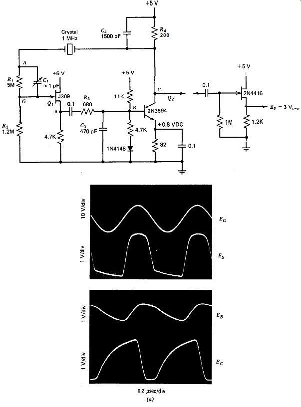
Figure 10.6(a). High-resistance load circuit at 1 MHz.
.... voltage divider ratio (i.e., reducing R2) at the FET input would help square up the waveform.
When the FET amplifier saturates on the positive signal peaks, the only effect on the crystal is that its capacitive load increases from 5.8 to 6.0 pF. Amplifier gain from point A to point C in Fig. 10.6~ is only 0.8X, and additional gain for circuit oscillation is provided by partial resonance of part of the crystal's inductance with the series combination of C, and the FET's input capacitance of 4 pF.
What sort of load does the crystal see in this circuit? It sees a capacitive load, consisting mostly of the crystal's own terminal capacitance C, (about 5 pF). The FET has an input capacitance of 4 pF directly across R,. To frequency compensate the voltage divider, about 1 pF is added across R,. The impedance of these two capacitors at 1 MHz is much lower than the resistance values of R, and R2, which means that the voltage divider is effectively capacitive rather than resistive.
Figure 10.6. Equivalent crystal load for high-resistance load circuit: (b)
crystal load circuit, (c) intermediate, and (d) equivalent load circuits.
Due to the small 5-pF capacitance of the load effectively in series with the crystal, the oscillation frequency is 670 ppm higher than it would be with a low impedance load; this is as expected. Figures 10.6b-d show the equivalent circuit. As can be seen from Fig. 10.6d, the equivalent I series RC load on the crystal is 122 R and 5.8 pF. The crystal's internal series resistance R, is 240 R, so that the external 122 R adds about 50% more, a reasonably small amount in practice. Figure 10.6 shows that most of the external 122-R load resistance comes from the high resistance voltage divider, which means voltage-divider resistances I could have been higher. Higher values of 10 and 2.4 M-ohm, respectively, for R 1 and R, would have reduced equivalent series load resistance in half, to 61 R, a reasonable improvement in circuit Q.
This circuit provides a good example of what happens when we put a high resistance load on the crystal. The resonant frequency rises significantly, and a 90 degr. phase lag occurs that must be compensated for in the amplifier. The 90 degr. phase lag is due to measuring the crystal current by means of the voltage across a capacitor (effectively) rather than across a resistor. Two RC networks R,C, and R,C, are added internally in the amplifier, with each providing 45 degr. of phase lag. Transistor Q2 inverts the signal, giving a total of 360 degr. phase shift around the loop.
10.7. COMMON BASE-TRANSISTOR
The schematic of this circuit at 1 MHz is shown in Fig. 10.7. The circuit works very nicely. The crystal's internal series resistance R, is 240 ohm , driving impedance is 10 a, and load impedance is 40 ohm. The in-circuit Q is degraded from the crystal's internal Q by (240 + 40 + lo)/ 240 = 1.2, which is quite reasonable. Waveforms at points A and B in Fig. 10.7~ show that both transistors stay on over the complete waveform cycle, maintaining their low source and load resistances. The diode amplitude clamp works very well in this circuit. This common base oscillator circuit can be used up to 20 MHz by decreasing the emitter input resistance of Q 1 at point A in order to provide the lower load resistance needed by the crystal at higher frequencies. Increasing the emitter current of Q, will decrease its emitter input resistance.
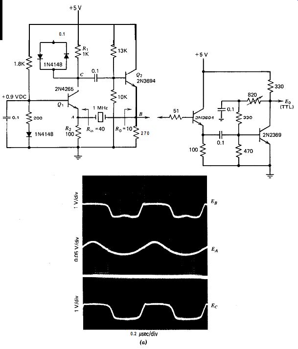
Figure 10.7(a). Common base circuit at 1 MHz.
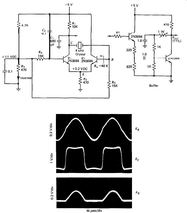
Figure 10.7(b). Common base circuit at 4 kHz (R, = 45KR). For operation at
50 kHz (R, = 20K a), use R, = R, = R., = 4.7K R and C, = 220 pF.
Figure 10.7b shows a low frequency variation of the common base amplifier circuit operating at 4 kHz. This circuit also works very well.
Here, the crystal is moved to a higher impedance point between collector and base, and the two emitters are tied together. The 4-kHz crystal's internal series resistance is 45K R, the source resistance is half of R, or 5K R, and the load resistance is 11K a. This gives an in-circuit reduction of the crystal's internal Q of (45K + 5K + llK)/ 45K = 1.4, a reasonable value. The capacitor C1 is added to the circuit to reduce noise at the sine wave cross-over switching points in order to avoid multiple on-off switchings of Q2 due to noise. This circuit also works well at 50 kHz by using circuit values given in the caption to Fig. 10.7b.
The emitter waveform at point E in Fig. 10.7b is rather interesting; it looks like the output of a half-wave rectifier. The half sine wave occurs when the base of Q2 goes positive, pulling up the emitter voltage at point E. The waveform goes flat when the base of Q2 goes negative and turns Q2 off, which pulls Q1 into a full-on state.
10.8. COMMON BASE-F'ET
The schematic of this circuit at 1 MHz is shown in Fig. 10.8; this circuit works very nicely. The l-MHz crystal's internal series resistance is 240 R, source resistance is 10 R, and load resistance is 200 a. This gives an in-circuit Q reduction of (240 + 200 + lo)/240 = 1.9. A high transconductance FET like the 5309 or U309 is required to get the FET's source input resistance down to 200 R. At. lower frequencies, where a higher crystal load resistance is desired to avoid excessive gain loss, a FET of normal transconductance like the 2N4416 will provide a source input resistance of about 500 s1. Waveform photographs show that both the FET and transistor stay in the linear region and maintain constant source and load resistances for the crystal over the complete waveform cycle.
This is due to the use of the diode clamp for voltage limiting.
10.9. PIERCE
The schematic of this circuit for 1-MHz operation is shown in Fig. 10.9a; the circuit works very well. One criticism is that the crystal's driving waveform could be more symmetrical than it actually is. The short-term stability measures a very good 0.1 ppm.
Figures 10.9b and c show the equivalent series RC load seen by the crystal in Fig. 10.9. The output resistance of the transistor stage is aver aged at 500 ohm, halfway between the on- and off-state values of 0 and 1000 a, respectively. Figure 10.9 shows that the crystal's equivalent series load resistance is a low 25 a. This is only 10% of the crystal's internal series resistance of 240 R, so that in-circuit Q is only 10% less than the crystal's inherent Q. The low equivalent load resistance with respect to the crystal's internal series resistance R, is the primary reason for the Pierce circuit's very good short-term frequency stability.
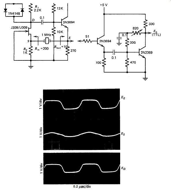
Figure 10.8. Common gate circuit at 1 MHz.
To get a higher crystal load resistance (R,,) of 500 ohm at lower frequencies, substitute 2N4416 for U309, and use R,
= 3.3KR, R2 = 1.5KR.
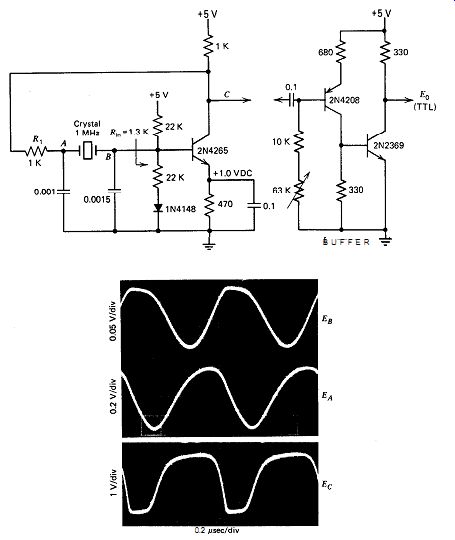
Figure 10.9 (a).
Pierce at 1 MHz.
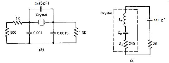
Figure 10.9 (b-c).
Equivalent crystal load for the 1-MHz Pierce circuit in Fig. 10.9a:
(b) crystal load circuit and (c) equivalent circuit.
A schematic for a low frequency Pierce circuit at 4 kHz is shown in Fig. 10.W. The main change here is the use of a FET source follower to avoid loading the crystal, which has a high internal resistance R, of 45K
a. This circuit works very well.
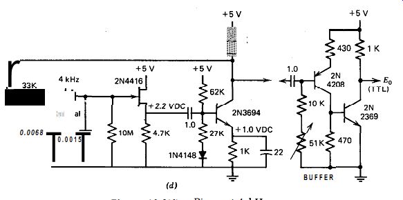
Figure 10.9(d). Pierce at 4 kHz.
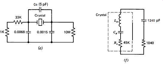
Figure 10.9. Equivalent crystal load for the 4-kHz Pierce circuit in Fig.
10.9d:
(e) crystal load circuit and (f) equivalent load circuit.
Figures 10.9e and f show the equivalent series RC load seen by the crystal in Fig. 10.9d. The output resistance of the transistor stage is averaged at 1000 ohm, halfway between the on- and off-state values of 0 and 2000 ohm, respectively. Figure 10.9f shows that the crystal's equivalent series load resistance is only 1040 ohm, about 2% of the crystal's internal series resistance of 45K R. This means that in-circuit Q is down only 2% from the crystal's inherent internal Q.
A schematic for a high-frequency Pierce circuit at 20 MHz is shown in Fig. 10.9g; this circuit works very well also. In this circuit, two emitter followers have been added at the amplifier output to permit driving the low impedance crystal circuit. The 2N2369 requires a heat sink. R, is selected on the basis that 30 R is the smallest resistance that the 2N2369 can drive without distortion. One change that might be made in this circuit would be to replace the 2N2369, which draws a lot of current, with a step-down transformer. This would raise the low impedance of the crystal circuit to something the 2N5179 emitter follower could drive directly.
Figures 10.9h and i show the equivalent series RC load seen by the crystal at 20 MHz in Fig. 10.9g. The equivalent series load resistance is 1.8 a, which is only 12% of the crystal's internal series resistance of 15 R.
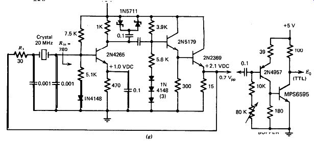
Figure 10.9(g). Pierce at 20 MHZ.

Figure 10.9. Equivalent crystal load for the 20-MHz Pierce circuit in Fig.
10.9g: (h) crystal load circuit and (i) equivalent load circuit.
The in-circuit Q of this 20-MHz Pierce circuit is down only 12% from the crystal's inherent internal Q.
10.10. PIERCE AT EXACT SERIES RESONANCE
The schematic of this circuit at 1 MHz is shown in Fig. 10.10. Three 60 degr. RC lag networks are used to generate the 180 degr. phase shift needed to operate the crystal at exact series resonance. It is convenient to increase R, to 100 0 to give the emitter follower Q2 an easier load to drive. This raises the R,C, phase shift from 60 to 70 degr. To compensate for this, the R,C, phase shift is decreased from 60 to 50 degr. A heat sink is required for the emitter follower Q2. C, is selected so that its phase shift with the crystal's internal series resistance R, is 60 degr. This circuit works very well and shows a 0.1-ppm frequency stability.
Figure 10.10b and c show the equivalent series RC load seen by the crystal in Fig. 10.10. The equivalent series load resistance is only 18 ohm or 8% of the crystal's internal series resistance of 240 R. This means that in-circuit Q is only 8% lower than the crystal's inherent internal Q.
Do we gain anything by operating the crystal at exact series resonance instead of just near it? Yes and no. One advantage of the exact series resonant circuit is its lower loop gain losses, which permit using a lower-gain transistor. There may or may not be a difference in the crystal's long-term drift stability by operating it at exact series resonance;
short-term stability measures about the same. The exact resonance circuit is more complex, however, since it uses two transistors instead of one and three RC networks instead of two. With a little more design work, it might be possible to eliminate the second transistor.
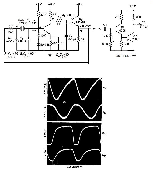
Fig. 10.10(a). Pierce at exact series resonance, at 1 MHz.
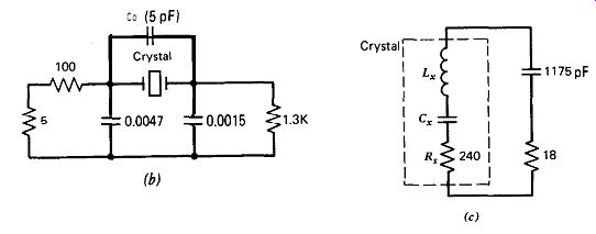
Figure 10.10. Equivalent crystal load for the 1-MHz Pierce circuit in Fig.
10.10a: (b) crystal load circuit and (c) equivalent load circuit.
10.11. PIERCE WITHOUT SERIES RESISTOR
The standard Pierce circuit in Fig. 10.9~ is occasionally seen without the series resistor R,. This reduces gain losses in the circuit and allows operation with a medium gain transistor instead of the high-gain transistor required by the standard Pierce circuit. The main drawback is that the crystal operates at a higher voltage level. If the circuit is used above 4 MHz, the crystal's power dissipation should be checked in order to be sure it is within the dissipation limit.
Figure 10.11~ shows a Pierce oscillator circuit without the series resistor R,. This circuit is identical to the one in Fig. 10.9a except that R, is eliminated. Waveform photographs in each figure allow a direct comparison of the difference. When R, is eliminated, its function in the R,C, phase-shift network in Fig. 10.11a is replaced by the parallel resistance of R, and the output resistance of Q,'s collector.
Figures 10.11b and c show the equivalent series RC load seen by the crystal. The equivalent series load resistance is 54 Q or 23% of the crystal's internal series resistance of 240 ohm. This gives an in-circuit Q only 23% lower than the crystal's inherent internal Q.
10.12. EMITTER COUPLED
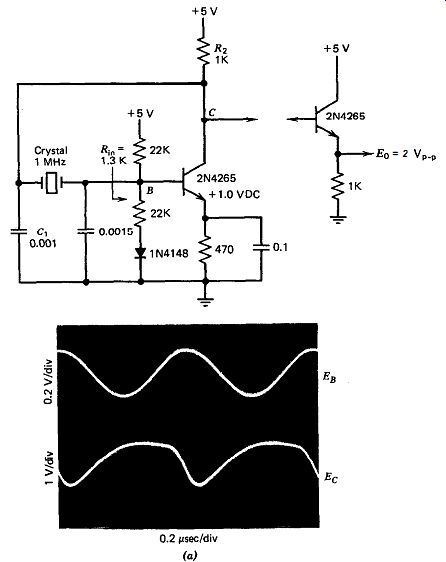
Figure 10.11(a). Pierce without a series resistor, at 1 MHz.
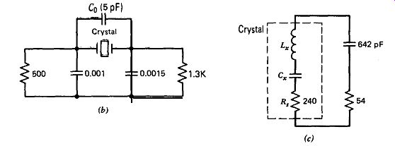
Figure 10.11. Pierce without a series resistor, at 1 MHz: (a) schematic, (b)
crystal load circuit, and (c) equivalent crystal load circuit.
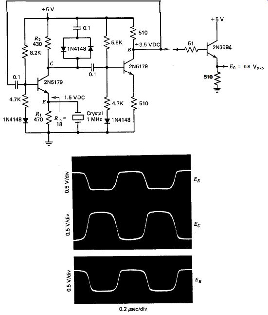
Figure 10.12. Emitter coupled circuit at 1 MHz.
The schematic of this circuit at 1 MHz is shown in Fig. 10.12. This circuit works fairly well and has a very good short-term frequency stability of 0.1 ppm. The crystal also has a good waveform across it.
The loop gain with the crystal removed from the circuit is set at slightly less than 1X (about 0.8X). The ratio of collector to emitter resistances in the first stage is 0.9, and loading effects from the second stage cut the actual first stage gain another 10% to 0.8X. The second stage has a gain of 1X and inverts the signal to provide positive feedback. The 1-MHz crystal has an internal series resistance R, of 240 R. The emitter resistor shunting the crystal is set at about twice the crystal's internal resistance or 470 R. Because the loop gain is just short of 1X over a wide frequency range, circuit waveforms are sensitive to stray capacitance effects.
To obtain a good waveform across the crystal, a diode amplitude clamp must be used across the collector resistor R, in the first stage. The resulting low signal amplitude prevents the emitter current from going to zero and keeps the crystal's load resistance at a desirably low value.
The crystal's low load resistance is the transistor emitter's input resistance R,,, which is 18 ohm in Fig. 10.12. This low load resistance on the crystal is the primary reason for the circuit's very good short-term stability. If the emitter current were to go to zero, the load on the crystal would increase from the 18-R input resistance of the emitter to the 470 ohm of the emitter resistor R,. The diode clamp also keeps the first stage transistor from saturating, which would increase the crystal's load resistance if it occurred.
10.13. MODIFIED MEACHAM
A schematic of the modified Meacham half-bridge circuit at 1 MHz is shown in Fig. 10.13 a. It is a complex circuit with good performance and operates at series resonance. Its short-term frequency stability is particularly good, being as good as or better than 0.1 ppm, the limit of available measuring equipment. It was not possible to tell whether the 0.1-ppm frequency variation observed was in the circuit or the frequency-measuring equipment. Figure 10.13b shows voltage waveforms at various points in the circuit. The somewhat peculiar waveform shown at the bridge output (E, in Fig. 10.13b ) is normal and results from the bridge subtracting a square wave with sloping sides (through bridge arm R,) from a sine wave (through the crystal arm).
The circuit uses a two-stage amplifier, with a gain of 28X from point A to point B in Fig. 10.13~. The split-load phase inverter Q, provides a 2 to 1 half-bridge, with the emitter resistor twice as large as the collector resistor. C2 is twice as large as the crystal's shunt terminal capacitance co of 3.5 pF in order to balance the half-bridge capacitively. C, is more important than it looks, since the signal path through Co provides positive feedback, which tends to make the amplifier oscillate, while the signal path through C, provides negative feedback and stabilizes the amplifier. C1 improves the high-frequency phase response of Q,'s collector, so that its high-frequency response is flat out to 80 MHz. The value of C, is determined experimentally, and its use helps considerably in pre venting high-frequency parasitic oscillation.
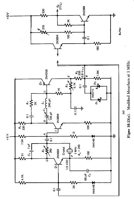
Fig. 10.13
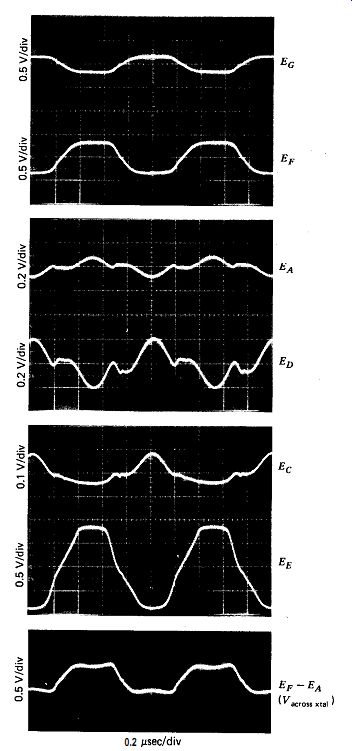
Figure 10.13(b). Waveforms for modified Meacham circuit in Fig. 10.13.
For maximum frequency stability and maximum in-circuit Q, it is desirable to use the smallest possible value of R,. With a 2 to 1 half-bridge, the minimum theoretical value of R2 for the circuit to oscillate is equal to one-half the crystal's internal series resistance R,. The 1-MHz crystal used has an internal resistance of 240 a, so the minimum value for R2 is 120 s1. The circuit will not oscillate except parasitically when R, is less than its theoretical minimum value of 120 R, so this condition makes a good test for parasitics. The circuit in Fig. 10.13 does not oscillate when R2 is less than 120 R, indicating a stable amplifier design. In practice, R2 has to be slightly larger than 0.5 R, for the circuit to oscillate, the exact amount depending on amplifier gain. In Fig. 10.13 , a practical value for R, is 290 ohm, a small amount more than the bare minimum needed for oscillation, to ensure that the circuit will oscillate under all conditions.
This gives a ratio of practical to theoretical minimum values of 290/120 or 2.4. This ratio of 2.4 for 2R2/R, provides a measure of the crystal's in circuit Q, with the unattainable ratio of one corresponding to infinite Q.
The amplifier stage Q2 is designed to present a reasonably high load resistance to the half-bridge and drive the relatively low input resistance of Qs's base-emitter junction. The second amplifier stage drives the diode clamp, D1-D2. Resistor R, provides a source resistance for the diode clamp to work against. The feedback resistor R, adjusts the on/off ratio of the clamped square wave to 1.0.
The circuit uses one resonant LC circuit, tuned to the frequency of oscillation, to reduce the circuit's frequency response away from resonance. Tuning the LC circuit has a considerable effect on the circuit's oscillation frequency, so both L, and C, must be stable components. L, must be an air core inductor, and C, must be adjustable to 1% for close tuning. Note that L,C, is shunted by a resistance R,, which corrects the 90 degr. phase shift of L,C, back to 0 degr. at frequencies far away from resonance.
This helps stabilize the circuit and prevent parasitic oscillation.
Figure 10.13~ shows a modified Meacham circuit for lo-MHz operation. This circuit performs well; its short-term stability is 0.1 ppm, at the limit of available measuring equipment. The circuit uses a three-stage amplifier that is different in several respects from the one used at 1 MHz.
The differences are primarily due to the crystal's much lower internal series resistance R, at 10 MHz. First, the split-load phase inverter Qr has much lower emitter and collector resistors, so that Qr can drive the low 5-R resistance of the 10-MHz crystal. Second, an emitter follower Q4 has been added to drive the low input resistance of the phase inverter Qr.
And third, the L,C, tank circuit for rolling off frequencies away from resonance has been moved to the emitter of Q,, where it increases the gain of Q2 at frequencies near resonance. The base input resistance of Q2 is low with this arrangement, but it is still relatively high with respect
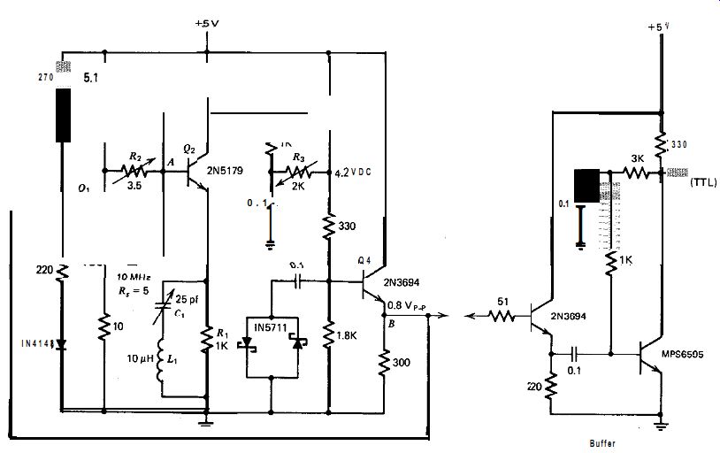
Figure 10.13(c). Modified Meacham at 10 MHz.
to the very low resistance of R2 and the crystal's internal resistance R,, so it does not load the half-bridge significantly. L,C, is deliberately shunted with R, in order to reduce the 90 degr. phase shift of L1C1 at frequencies far away from resonance back to 0".
The circuit uses a 2 to 1 half-bridge, so C, in Fig. 10.13b is set equal to twice the crystal's shunt terminal capacitance C, of 8.5 pF. The theoretical minimum value of R, in this circuit is 0.5 R, or 2.5 R. The practical value of R,, set at just slightly more than the minimum value for oscillation, is 3.5 IR. This gives a practical to theoretical minimum ratio of 3.5 t 2.5 or 1.4 for R,.
The voltage gain of the amplifier from point A to point B in Fig. 10.13 is 50X. The amplifier is stable and does not oscillate when R, is set below its minimum theoretical value for oscillation of 2.5 R. A heat sink is required on transistor Q1.
Figure 10.13d shows a modified Meacham circuit for 100-kHz operation. This circuit works well and has a short-term frequency stability of 0.1 ppm, at the limit of available measuring equipment. The circuit uses a three-stage amplifier and differs in several respects from the one used at 1 MHz, primarily because of the crystal's higher internal resistance at 100 kHz. An emitter follower Q4 is used at the bridge output to prevent the amplifier from loading the bridge. The tuned circuit L1C1 is moved to the emitter of Q2 and increases the gain of Q2 at resonance. The low input resistance of Q2 at resonance is easily driven by the emitter follower Q4.
L,C, is shunted with a resistor R, to reduce the 90 degr. phase shift of L1C1 at frequencies far away from resonance back to 0 degr.
Q3 is a combination amplifier and diode amplitude clamp and gives a fixed on/off ratio to its square wave output that is very close to 1.0. The on/off ratio is independent of power supply or bias changes. R, trims the waveform flatness at the top and bottom of the square wave out of Q3.
Because of the 2 to 1 bridge ratio set by Q1's emitter-to-collector resistance ratio, C, is set equal to twice the crystal's terminal shunt capacitance C, of 8 pF. The theoretical minimum value of R, is one-half of the crystal's internal series resistance R, or 200 a, again because of the bridge's 2 to 1 ratio. The practical minimum value of R,, set at slightly more than the minimum required for oscillation, is 420 R. This gives a practical-to-theoretical minimum ratio of 420/200 or 2.1 for R, in Fig. 10.13d. The amplifier is stable and does not oscillate when R, is set below the minimum theoretical value for oscillation. The amplifier has a gain of 100X from point A to point B in Fig. 10.13d.
------------
Although the modified Meacham circuits described here work well, the amplifiers used in them can probably be simplified and improved.
One approach would be to combine the best parts of the three amplifiers into one. Such an amplifier would include: (1) a shunt capacitor C, across the Q, phase splitter's emitter resistor to correct the high-frequency phase response at the phase splitter's collector, as in Fig. 10.13~; (2) a series L,C, network across Q2's emitter resistor R, in order to amplify only the desired oscillation frequency, as in Figs. 10.13 and d; and (3) putting the diode amplitude clamp between Q3's base and collector, as in Fig. 10.13d. Another approach would be to put the L,C, filter after the diode amplitude clamp in the amplifier, so that the crystal is driven with a sine wave instead of a square wave.
C. HARMONIC CIRCUITS
10.14. COLPITTS (20 MHz)
The schematic of this harmonic oscillator is shown in Fig. 10.14. This 20-MHz harmonic circuit is the same as the 20-MHz fundamental circuit shown in Fig. 10.4d except that the 390-n emitter resistor R, is replaced with a 3.2~PH inductor whose impedance (410 n at 20 MHz) is approximately equal to the resistance of R1. The bias resistor R, is also increased to 470K ohm, to accommodate the DC voltage shift when R, is removed.
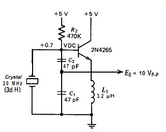
Figure 10.14. Colpitts harmonic circuit at 20 MHz. Crystal shunt resistance
must be 2 22K R for no loading effects and 2 2.2K R for oscillation to occur.
The voltage swing at both the base and emitter terminals is a large 10 Vp-p (+5 to -5 VDC).
Circuit performance is rated fair. The strong point of this circuit is its low parts count. Its frequency is somewhat sensitive to power supply changes, however. In an effort to reduce this sensitivity, the base biasing resistor R, was replaced with a FET constant current source, but this did not help.
10.15. BUTLER COMMON BASE (20 MHz. C-TAP)
The schematic of this VHF harmonic oscillator is shown in Fig. 10.15.
The crystal operates at its third harmonic. Bad parasitics seem to be inherent in the Butler common base circuit, and it requires considerable experimental effort to come up with a satisfactory parts layout. Even then, several parasitics usually remain. We end up satisfied if the tank circuit will tune properly without spurious oscillations just at the frequency desired. R, and R, help damp down parasitic effects considerably and also help isolate external load-capacitance effects from the tuned circuit.
Diode D 1 helps stabilize the collector current against a varying power supply voltage, but it does not help enough. The collector current still varies too much. The circuit works better (less lead inductance?) if C, is tied directly to the grounded end of the emitter resistor R,, as shown in Fig. 10.15, rather than to +5 VDC, as shown in Fig. 5.28. The emitter waveform shows that the transistor does not cut off and, thus, provides a reasonably constant low resistance load to the crystal over the complete waveform. The diode clamp ensures that the transistor does not saturate and keeps the oscillation amplitude within the transistor's linear region.
The crystal's load resistance is about 10 ohm , and its internal series resistance is about 40 R. This gives a voltage-divider gain loss of 10/( 10 + 40) or 0.20. The crystal's capacitive source impedance is between one and two times the impedance of C, (35 a), depending on the value of C,. The circuit's frequency sensitivity to temperature depends on the collector current and varies two to one over the operating range of collector current.
To oscillate properly, the collector current must be set at a specific value. Below this value, the circuit will not oscillate; above this value, oscillation ceases. If the emitter current is increased even further, the circuit will start oscillating again at some other frequency, either at a harmonic or at some other spurious frequency.
Waveforms in Fig. 10.15 show a 40 degr. phase lag from point E to point C and a 60 degr. phase lead from point C to point A, with the crystal and its resistive load providing a 20 degr. phase lag from point A to point E. Tuning C, will change the crystal's phase shift from lag to zero (series resonance) to lead, with the other two phase angles changing accordingly, so that they always add up to zero.
--------------
This circuit works satisfactorily once we get past the parasitics. But its basic design defect of oscillating only over a narrow range of collector current, and its bad parasitics, make it only a poor to fair circuit.
10.16. BUTLER COMMON BASE (20 MHz. L-TAP)
The schematic of this VHF harmonic oscillator is shown in Fig. 10.16.
The purpose of this circuit is to find out if an inductive tap offers any thing useful over a capacitive tap. The circuit is the same as the one in Fig. 10.15 except that the crystal is tapped down on the inductor in the LC tank instead of on the capacitor. The biggest advantage of the L tapped circuit is that it has no parasitics (assuming a reasonable parts layout), which makes it much easier to debug and tune. The biggest disadvantage is a lower oscillation frequency. The inductive tap introduces a phase lag in the circuit in comparison with a capacitive tap, which introduces a phase lead. The crystal must provide a large phase lead to compensate for the two phase lags of the LC tank circuit and the inductive tap (see Section 7). To provide the phase lead, the crystal must operate below series resonance, which is what gives the circuit its lower oscillation frequency. The phase lag from E to C in Fig. 10.16 is 50 degr. From C to A, the phase lag is 22 degr., and the crystal and its emitter load provide a 72 degr. phase lead from A to E.
The frequency-temperature sensitivity varies 2 to 1 with the emitter current in both the L-tap and C-tap circuits. A minor disadvantage of the L-tap circuit is that it is harder to check. Putting the capacitive load of a scope probe (about 7 pF) at the inductive tap point A in Fig. 10.16 disturbs the circuit and adds unwanted oscillatory ripples to the waveform.
The circuit's overall performance is about the same with an inductive tap as with a capacitive tap. Either way, the circuit is rated only as a poor to fair VHF harmonic oscillator.
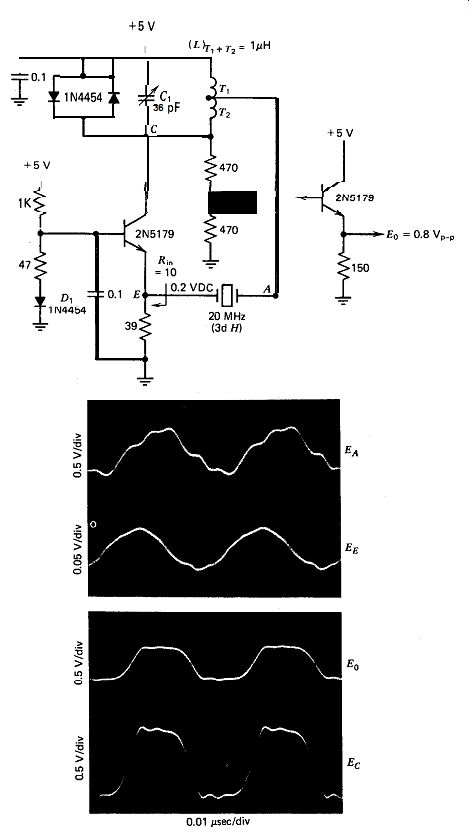
Figure 10.16. Butler common base at 20 MHz, inductive tap. T, = 7 turns, T2
=19 turns.
10.17. BUTLER COMMON BASE (50 MHz)
The schematic of this VHF harmonic oscillator, shown in Fig. 10.17, exhibits parasitic effects typical of this circuit. The 50-MHz third-harmonic crystal used had a relatively low series resistance of 25 R. The crystal's load impedance is 8 a. The crystal's capacitive source impedance is one to two times the impedance of C, (70 a), depending on the setting of C,.
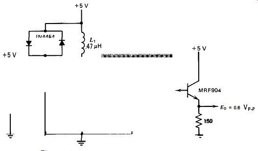
Figure 10.17. Butler common base at 50 MHz.
The diode amplitude clamp across L, is very effective in keeping the emitter drive voltage low, so that the transistor will stay in its linear region. The emitter then provides a low and constant load resistance to the crystal over the complete waveform cycle.
Circuit performance is only fair to poor due to its design defect of oscillating over only a narrow range of collector current and its bad parasitic effects.
10.18. BUTLER COMMON BASE (100 MHz. C-TAP)
The schematic of this VHF harmonic oscillator is shown in Fig. 10.18.
The crystal operates at the fifth harmonic. Diodes D,-D, provide a stabilized bias voltage source for the transistor. Diodes D, and D, limit oscillation amplitude and keep the transistor from saturating or shutting off at any part of the waveform cycle. The crystal's internal series resistance R, is 70 a, and its load impedance is 8 a. The crystal's capacitive source impedance is one to two times the impedance of C, (100 a), de pending on the value of C,. The circuit can be set to exact series resonance by tuning C, so that the voltages at points A and E in Fig. 10.18 are in phase with each other. This assumes that the emitter's input impedance at E is a pure resistance and not reactive.
An adjustable inductor L2 is placed across the crystal to tune out the crystal's terminal capacitance C, of 5.7 pF. L, can be an iron-core inductor, but L, must be an air-core unit. The circuit will still oscillate if L, is not used, but frequency sensitivity to power supply variations is four times worse, and short-term frequency stability also degrades somewhat.
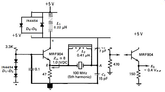
Figure 10.18. Butler common base at 100 MHz, capacitive tap.
The performance of this circuit is only fair to poor due to the usual parasitics with this circuit and the circuit's design defect of oscillating over only a narrow range of collector current.
10.19. BUTLER COMMON BASE (100 MHz. L-TAP)
The schematic of this VHF harmonic oscillator is shown in Fig. 10.19.
The purpose of this circuit is to try out Butler's idea [6] of canceling the crystal's terminal capacitance C, by adding an equal voltage of opposite phase through an equivalent capacitance C, to the crystal's output at the emitter. The opposite phase is obtained by extending L, a few turns be yond the normal +5 V power supply end of the coil.
The terminal-capacitance cancellation idea works poorly. ,The L, taps at T, and T, are low impedance. Circuit operation is quite sensitive to the length of the common lead wire from A and B in Fig. 11.19, which was about a half-inch long in the test circuit. Some sort of common mode effect in the common lead wire from A to B (probably lead inductance) seems to be present and requires an excessively large reverse-phase voltage (T, > T,) and a compensation capacitance C, that is 25% larger than the crystal's terminal capacitance C, to cancel out C,. In addition, the oscillation frequency is unnecessarily sensitive to small changes in C, or C,.
This circuit performs poorly. The idea of canceling out the crystal's
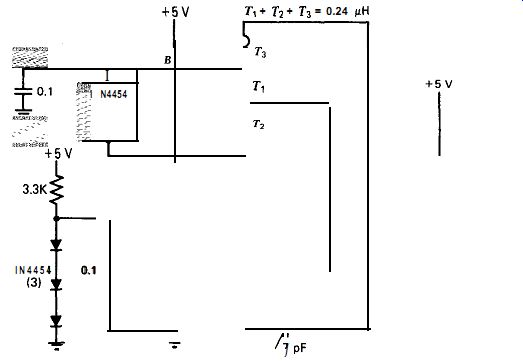
Figure 10.19. Butler common base at 100 MHz, inductive tap. T, = 1.2 turns,
T, = 2.6 turns, T3 = 2.2 turns.
terminal capacitance with a capacitance bridge circuit does not work well in practice.
10.20. BUTLER EMITTER FOLLOWER (20 MHz, C-TAP)
The schematic of this VHF harmonic oscillator is shown in Fig. 10.20.
The crystal operates at the third harmonic and is tapped into the capacitive side of the LC tank. The circuit has no parasitic effects of any kind.
There are no 2.6 V Zener diodes available, so four signal diodes are cascaded in series for base biasing. The emitter's output resistance that drives the crystal is 25 R. The crystal's load impedance is mostly capacitive and is one to two times the impedance of C, (35 a), depending on the value of C,. The crystal's internal series resistance R, is 40 a.
This circuit works very well, and the absence of parasitics is a big help. By tuning C,, the oscillation frequency can be set either at or slightly above (2 ppm) series resonance.
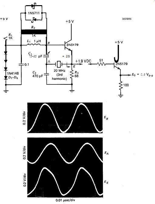
Figure 10.20
10.21. BUTLER EMITTER FOLLOWER (20 MHz. L-TAP)
The schematic of this VHF harmonic oscillator is shown in Fig. 10.21.
The purpose of this circuit is to find out if an inductive tap offers any thing more than a capacitive tap does. The crystal operates at the third harmonic. The circuit is essentially the same as the one in Fig. 10.20 except that the crystal is tapped down on the inductor in the LC tank instead of on the capacitor. The inductive tap introduces a phase lag in the circuit, as compared with a capacitive tap, which introduces a phase lead. The crystal must provide a phase lead to compensate for the phase lag of the inductive tap, which means that the crystal must operate below resonance. This gives the circuit a lower oscillation frequency compared with the capacitive tap circuit.
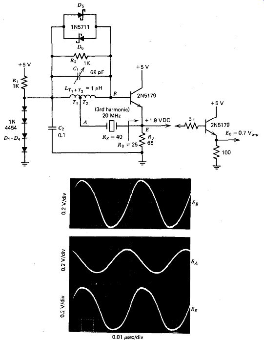
Figure 10.21. Butler emitter follower at 20 MHz, inductive tap. T, = 4 turns,
T2 = 22 turns.
There are no 2.6 V Zener diodes available, so four signal diodes are cascaded in series for base biasing. The emitter's output resistance driving the crystal is 25 0. The crystal's load impedance is mostly inductive and one to two times the 30-a inductive reactance of the tapped portion T, of the 1-PH inductor. The crystal's internal series resistance R, is about 40 R. For good operation, the circuit requires a short coupled bypass capacitor C2 from the "grounded" end of the inductor to the grounded end of the emitter resistor RS, as shown in Fig. 10.21.
This circuit works very well, but it does not offer any advantages over the C-tap circuit. Neither the L-tap or C-tap circuits show any parasitic oscillation effects. However, the oscillation frequency with the L-tap is always slightly below series resonance (about 2 ppm). Tuning C, will vary the oscillation frequency from 3 to 1 ppm below series resonance.
Why this circuit will not oscillate at series resonance is not known.
The analysis in Section 7 indicates that it should be possible. Removing the diode amplitude clamp D,-De will allow the circuit to oscillate at series resonance or even up to 2 ppm above it. But the emitter follower's source resistance that drives the crystal goes too high (the transistor shuts off over part of the oscillation cycle) for this to be a viable alternative.
Figure 10.22. Butler emitter follower at 50 MHz.
10.22. BUTLER EMITTER FOLLOWER (50 MHz)
The schematic of this VHF harmonic oscillator is shown in Fig. 10.22.
The crystal operates at the third harmonic and is tapped into the capacitive side of the LC tank. As is typical of this circuit, it has no parasitic oscillation effects. Since there are no 2.6 V Zeners available, four signal diodes in series are used for base biasing. The emitter's output impedance that drives the crystal is 29 a. The crystal's load impedance is mostly capacitive and one to two times the 40-52 capacitive reactance of C2, depending on the value of C,. The crystal's internal series resistance R, is 30 R. This is a good circuit and works very well without any problems.
10.23. BUTLER EMITTER FOLLOWER (100 MHz. C-TAP)
The schematic of this VHF harmonic oscillator is shown in Fig. 10.23.
The crystal operates at the fifth harmonic and is tapped into the capacitive side of the LC tank. As is typical of this circuit, it has no parasitics.
Since 2.6 V Zeners are not available, four signal diodes are cascaded in series for base biasing. The emitter's output impedance driving the crystal is 25 a. The crystal's load impedance is mostly capacitive and, depending on the value of Cr, is one to two times the 50 ohm impedance of G.
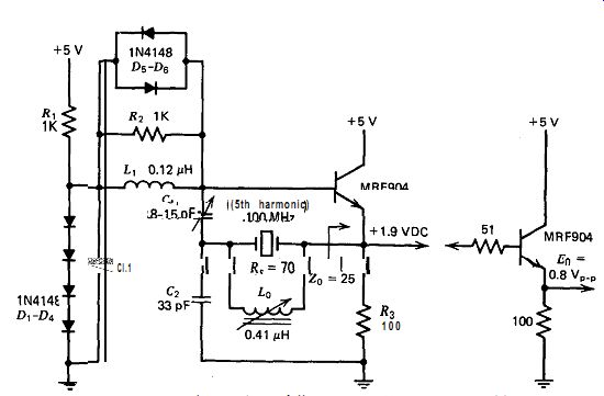
Figure 10.23. Butler emitter follower at 100 MHz, capacitive tap.
The crystal has a terminal capacitance Co of 4.2 pF and a capacitive reactance of 360 Q at 100 MHz. This is tuned out of the circuit by a 0.41 p henry inductor L, in parallel resonance across the crystal. The circuit will operate without the shunt inductor Lo, but the inductor provides a 4 to 10 times reduction in frequency sensitivity to power supply changes, which makes its use worthwhile. The oscillation amplitude at 100 MHz is low, so to give a larger oscillation amplitude fast-recovery signal di- odes rather than Schottky diodes are used for the amplitude clamp D,-Ds. This is a good circuit and works very well.
10.24. BUTLER EMITTER FOLLOWER (100 Mhz, L-TAP) , i
The schematic of this VHF harmonic oscillator is shown in Fig. 10.24.
The purpose of this circuit is to find out if Butler's out-of-phase subtraction scheme [6] for eliminating the crystal's terminal capacitance C, will work in the emitter follower circuit. The crystal operates at the fifth harmonic and is tapped into the inductive side of the LC tank. The crystal drive signal is fed through a capacitor C, to a reversed-phase tap on the inductor. If T1 equals T, and C, equals the crystal's terminal capacitance C,,, then the two capacitances will cancel out one another. I To set up the bridge balance, the crystal and C, are disconnected from the emitter and driven in parallel by an external signal generator at a frequency somewhere near (but not at) the oscillation frequency. C, is then adjusted for minimum signal at the emitter. The external signal generator is disconnected, and the crystal and C, are reconnected to the emitter. The circuit then oscillates at or near the crystal's series-resonant frequency.
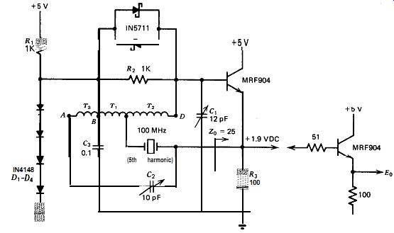
Figure 10.24. Butler emitter follower at 100 MHz, showing out-of-phase cancellation
of the crystal's terminal capacitance C,. LAD = 0.24 nH, 6 turns closewound
on 0.28-in. diameter form. T, = 1.2 turns, Tz = 2.6 turns, T3 = 2.2 turns.
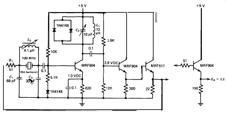
Figure 10.25. Pierce at 100 MHz.
This circuit does not work well at all; it performs poorly and tunes poorly. The out-of-phase cancellation idea works, but lopsidedly. At null balance, the capacitance C, is twice the crystal's terminal capacitance C,,, and T3 has twice the turns of T,. The circuit is very sensitive to the length (inductance?) of the ground lead in Fig. 10.24 from point I3 through the bypass capacitor C, to the grounded end of the emitter resistor R,, as if there were a common mode effect present. Changing C2 by 4 pF changes the oscillation frequency by 600 Hz, which is much too sensitive. And finally, the oscillation frequency of 99.996603 MHz is very low for a 100-MHz crystal.
10.25. PIERCE (100 MHz)
The schematic of this circuit is shown in Fig. 10.25. The crystal operates on the fifth harmonic. The first stage amplifier uses a tuned L,C, tank as the collector load, with a diode amplitude limiter. The second and third stages are emitter followers to drop the high L,C, tank impedance to about 5 ohm in order to drive the low impedance crystal circuit. L, has to have an air core in order to avoid the detuning effects of core saturation and its associated nonlinearities, but L, is less sensitive and can use an iron core. A heat sink is required on the MRF517.
The circuit works well and has relatively low sensitivity to power supply changes. The second emitter follower draws a large power supply current and is an obvious candidate for replacement by a step-down transformer in low power applications. The L,C, tank tunes satisfactorily, but parasitics show up quickly when detuned. The circuit has a relatively high parts count.