15.1 THE IDEAL AMPLIFIER
Amplification--the ability to use a low-power waveform to reproduce a higher-power copy of that waveform--is unquestionably the feat that gave birth to the art of electronics. The majority of electronic circuitry in use today consists of amplifiers in one form or another. We may be aware that the amplifiers normally treated in a basic electronics course have certain limitations, but it will be helpful to enumerate these in order to define the goal of producing a more nearly ideal high-performance amplifier.
Frequency Response: The ideal amplifier would respond equally to all frequencies from 0 Hz (dc) to any desired high frequency. Elementary amplifiers are capacitively coupled and do not respond to dc or very-low-frequency ac. High-frequency response of real amplifiers is also limited, dropping off somewhere in the range between 100 kHz and 10 MHz for low-power amplifiers of elementary design.
The ability to respond to high-frequency sine waves can also be expressed as the ability to respond quickly to a square or pulse input wave. For an amplifier without serious overshoot or ringing on the square-wave response, the relationship

(15-1)
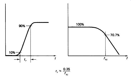
FIGURE 15-1 Rise time and frequency response are Inversely related If there
Is no significant overshoot or ringing.
...... where t r is the 10% to 90% rise time and fhi is the - 3-dB (0.707) high-frequency cutoff, as shown in Fig. 15-1.
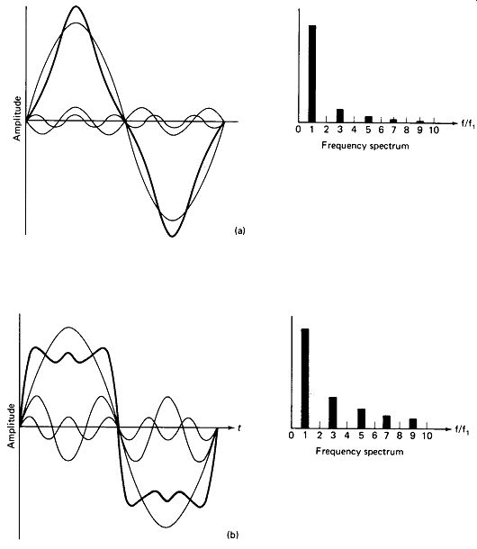
FIGURE 15-2 Triangle waves (a) and square waves (b), may be synthesized by
a fundamental and a series of harmonic sine waves.
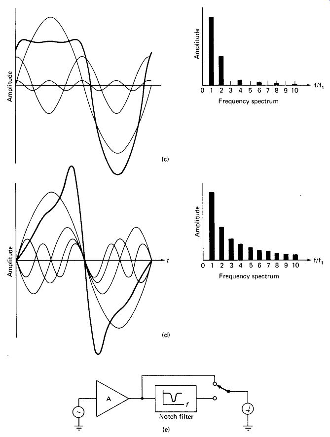
FIGURE 15-2 Half-wave rectified sine (c) and sawtooth waves (d) synthesized
from a fundamental and Its harmonics, (e) A Harmonic-distortion meter tunes
out the fundamental sine wave and measures the strength of the harmonics.
Harmonic Distortion: An ideal amplifier would produce an output waveshape that exactly reproduced the waveshape of the input, although the amplitude, phase, and polarity might be different. Real amplifiers always produce some waveshape distortion, even though it may be very slight in modern amplifiers. Consider the case of a 4500-km (2800-mi) transcontinental communications cable with a booster amplifier every 150 km. If each amplifier produced a 0.5% flattening of the waveform peaks (output peak 99.5% of input peak), the total output after 29 amplifiers would be 0.99579 , or 0.86, a flattening of 14%.
Amplifier distortion is not commonly measured as described above, but by percent harmonic distortion. This is based upon Fourier’s theorem that the only single-frequency waveform is the sine wave. All other waveshapes are composed of a fundamental-frequency sine wave with a number of harmonic (integer multiple) sine waves added. Figure 15-2 shows the Fourier spectrum (fundamental and relative strengths of harmonics) for triangle, square, half-wave rectified sine, and sawtooth waves, and gives a graphical addition of the first few harmonic sine waves. The ideal waveforms are approached as more harmonics are added.
Harmonic distortion measurement is accomplished by applying an extremely pure sine wave to the amplifier input, measuring the amplifier output, and adjusting an output meter , s sensitivity to read this as 100%. A very sharp filter is then switched in to eliminate the fundamental-frequency sine wave from the output, allowing only the aberrations (harmonics) to pass to the meter. The meter (ideally a true rms meter, but commonly just an average-responding voltmeter) then indicates percent harmonic distortion. It should be emphasized that any departure from the pure sine-wave shape, no matter how it is produced, actually consists of various harmonics of various amplitudes and phases added to a fundamental sine wave.
Only a pure sine wave is free of harmonics.
Voltage Gain: The ideal amplifier would have any desired voltage gain, and this gain would be variable by manual or electronic control. In practice, this is one of the easiest objectives to meet. The desired gain is built up by cascading several stages: four gain-of-10 stages to produce a gain of 10,000. Variable gain can be achieved in several ways: potentiometer voltage dividers, photoresistive cells, and changing bias points near the cutoff region for FETs can be employed to effect variable gain. As gains become very high (say, around 1000), undesired feedback via stray capacitance from output to input becomes a problem, and self-oscillation may result unless shielding and short straight-line signal paths are used.
Input Impedance: An ideal amplifier would draw absolutely no current from the signal source feeding it, which is to say that it would have infinite input impedance.
At low frequencies this ideal is easily realized with an FET input stage, but at high frequencies capacitive reactance becomes a problem. At 30 MHz, for example, the 5-pF input capacitance of the typical FET has a reactance of 1 k ohm.
Output Impedance: The output voltage of the ideal amplifier would not be limited by or reduced by the addition of a load resistance, no matter how much current it drew. Real amplifiers generally show a drop in output voltage when a load draws current from the output. Often there is also a maximum peak output current beyond which gross distortion of the output will become apparent.
Efficiency: Ideally, all the power an amplifier draws from its dc supply would be delivered as signal power to the load resistance. Actually, the amplifier components themselves consume considerable power. Efficiency is defined as _ signal power out V, dc power supplied In amplifiers delivering only 1-mW or so of power, the power waste of operating with an efficiency of 25% or even 2% is not objectionable. Audio amplifiers outputting 100 W and radio transmitters outputting several kilowatts are a different matter, however, and special pains are taken to get their efficiencies up to the 50 to 80% range.
15.2 NOISE REDUCTION
The detection of very weak signals--audio, radio, or otherwise--is never limited by lack of amplification. As we have seen, high amplification is simply a matter of cascading low-gain stages while taking reasonable care to isolate the outputs from stray coupling back to the inputs. The problem is always distinguishing the signal from the ever-present background noise. Once the signal level sinks down to the noise level, all attempts to amplify the signal will result in amplification of the noise as well. Anyone who has tried to tune in a weak TV station or listen to an AM radio during a thunderstorm is familiar with the noise problem.
Noise is of two basic types: environmental and inherent.
Environmental Noise, more properly called interference, can often be eliminated or avoided once its source is identified. Shielding, filtering, and frequency selection are the common techniques employed. Figure 15-3(a) shows how a short length of unshielded microphone line can pick up 60-Hz noise by a stray capacitive coupling of only 10 pF to the 120-V house wiring. You can verify the 23-mV result by calculating the voltage division of 120 V across 265 M-ohm capacitive in series with 50 k- ohm resistive. This example is not at all exaggerated, and high-impedance instrumentation pickups (1 M-ohm or 10 M-ohm) are even more susceptible to noise pickup. High-frequency noise (from switching transients, motor brushes, lamp dimmers, etc.) is also present on the ac line, and is coupled in more strongly because of lower capacitive reactance.
Figure 15-3(b) shows how shielding the line and the microphone couples the noise to ground rather than to the amplifier input. Figure 15-3(c) shows some common mistakes in shielding. The shielding enclosure should not simply be placed around the device with the wires protruding through a hole, nor should each enclosure and shielded cable be grounded separately. Rather, as shown in Fig. 15-3(d), the shielding enclosures should completely enclose each device, with the circuit ground connected to the shield at one point internally. Signal wires leaving the enclosure must run through shielded wire, with the shield mated to the metal enclosure to ensure no breaks in the enclosing of the signal wire. The entire system of boxes and cables should be earth-grounded at only one point on one of the cabinets. The continuous shield connections will take care of holding the cabinets at ground, and no extra noise will be introduced thereby.
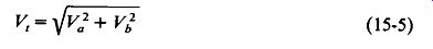
Figure 15-4(a) shows a motor brush-noise filter, which may keep high-frequency hash from entering the ac line, where it would be radiated all over. A simple capacitor, chosen to have a high reactance at audio frequencies but a low reactance to an interfering radio frequency, can often eliminate interference in tape or phone pickups, as shown in Fig. 15-4(b).
Frequencies to be avoided because of heavy concentrations of interference are:
. 60 Hz and its harmonics up to 300 Hz due to ac line radiation.
. 0.5 to 2.0 MHz because of AM broadcast and LORAN navigation transmitters.
. 27 MHz because of citizen’s band radio.
. 50 to 400 MHz because of broadcast TV, FM, police, and so on.
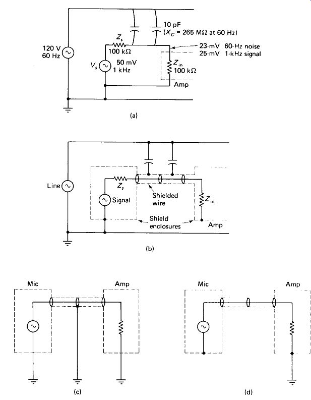
FIGURE 15-3 (a) Even a small stray capacitance to the ac line causes serious
noise pickup on a low-level high-impedance line, (b) Shielding eliminates noise
pickup, improper (c) and proper (d) shielding connections.
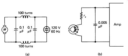
FIGURE 15-4 Noise-suppression techniques for a sparking-brush motor (a) and
a magnetic-tape or phono pickup (b).
Thermal Noise is a voltage produced across the terminals of any resistance because of the random thermal vibrations of the atoms constituting it. The frequency spectrum of thermal noise extends from dc to well above the frequency limit of electronic amplification techniques. Its amplitude is given by

15-3)
... where T is temperature in Kelvins (Celsius + 273), B is the passband of the amplifier between the upper and lower - 3-dB points in hertz, and R is the resistance in ohms. The peaks of the noise waveforms commonly reach four times the rms value. All resistive devices-bias resistors, receiving antennas, strain gages, semiconductors, and so on-produce thermal noise. It can be reduced by reducing the bandwidth of the amplifier or by lowering the temperature of the devices associated with the signal pickup. Indeed, space-probe receivers use very slow data rates (narrow bandwidth) and liquid nitrogen cooling to provide receivers capable of pulling the weakest possible signal from the noise.
EXAMPLE 15-1
What is the thermal noise produced by a 300-i television antenna at 27°C? The TV receiver has a bandwidth of 6 MHz.
Solution
This means that there is no possibility of receiving a TV station with an antenna signal of 5.5 /iV or less, even with ideal receiving equipment.
Shot Noise is produced at any junction or interface by the passage of the charge carriers. It is given by

, = V(3.2x 10"1,)/B
(15-4)
… where I is the junction current in amperes and B is the amplifier bandwidth in hertz. This suggests that the input stage of a sensitive amplifier should be operated at a low bias current for lowest noise generation,
and this is in fact the case.
EXAMPLE 15-2
What is the shot-noise voltage produced across the base-emitter junction of a transistor operated at an emitter bias current of 0.1 mA? The amplifier bandwidth is 6 MHz.
Solution
The ac resistance of the junction is found:
Flicker Noise or 1 //
Noise is produced by fluctuations in bias current, and has its strongest components at low frequencies, as the name implies. Above 1 kHz it is generally negligible, but frequencies below 100 Hz are often avoided in sensitive instruments to minimize its effects. It is most severe in semiconductors, so metal-film resistors may be chosen over carbon types in sensitive low-frequency instruments.
Low bias currents in the input stage will minimize flicker noise.
Addition of Noise Components from different sources cannot be carried out directly (Va + Vb), since the noise components at any instant may cancel rather than add.
Rather, noise adds by the sum of the squares of its components:
v, = yK, 2 + vbi
… where Va is the rms voltage of the first source, and so on.
(15-5)
15.3 NOISE SPECIFICATIONS
Signal-to-Noise Ratio, S/N, is more properly termed signal-plus-noise to noise ratio, (S + N)/N, since it is impossible in practice to achieve a noiseless signal, S.
An example will illustrate how the ratio is used.
Let us say that a receiver is tuned to 300 MHz with no signal at the antenna, and the volume is adjusted for a 1-V-rms noise output. A 4-uV signal is then applied (modulated with a 1-kHz tone) and the output rises to 2 V rms. We say that the receiver has a 4-uV sensitivity for a 2 : 1 (6-dB) signal-to-noise ratio.
Noise Figure, NF, is a measure of the deterioration in S/N ratio caused by an amplifier, mixer, or other signal processor. Ideally, it would be unity (0 dB), indicating that the amplifier simply amplified the input noise while contributing none of its own. It can be computed in two ways:
(15-6)
... where A is the amplifier power gain. Typical noise figures for well-designed transistor amplifiers are in the range 2 to 5 dB at 10 kHz, rising to perhaps 30 dB at 100 Hz because of flicker noise. As a rule of thumb, bipolar transistors give the lowest noise figure when operated with VCE 2 V and /c ss 0.1 mA, with a source impedance around 2 k ohm.
Equivalent Input Noise is sometimes specified as an alternative to noise figure for an amplifier. This is the input noise voltage that would have to be applied to the amplifier input to produce the observed noise output if the amplifier itself were noiseless.
Equivalent Noise Resistance is a second alternative to noise figure and is based on equation 15-3. The noise added by the amplifier is visualized as being due to a second fictitious resistance in series with the actual input source resistance. The thermal noise present at the input and the noise contributed by the amplifier can thus be compared directly as:
Ri/Rn,
... where Rn is the equivalent noise resistance.
Noise-Temperature Equivalent is a third alternative to noise figure, and is also based on equation 15-3. The two can be directly converted by the equation NF- +1 (15-7) .*O where Te is noise temperature, and Ta is ambient temperature, usually 20°C. Here the noise added by the amplifier is visualized as being due to a fictitious rise in the Kelvin temperature of the signal source resistance. Background noise from a radio receiving antenna is also often represented as being due to a fictitious rise in antenna temperature. This system has the advantage that all three noise sources (thermal, antenna background, and amplifier) can be represented in the same terms and compared and added directly.
Dynamic Range is an amplifier specification defining the ratio of maximum to minimum signals which the amplifier can faithfully reproduce. The upper limit is imposed by waveform (harmonic) distortion, 10% being the usually accepted figure.
The lower limit is imposed by signal-to-noise ratio, with a S/N voltage ratio of 10 (20 dB) taken as the usual standard. A dynamic range of 40 dB (100:1 voltage ratio) is readily achieved in audio amplifiers. A range of 70 dB (3000 : 1 voltage ratio) is considered exceptional.
15.4 VOLTAGE FOLLOWERS
While emitter-follower and source-follower amplifiers do not provide voltage gain, they do have advantages that make them indispensable in designing amplifiers approaching the ideal in performance.
. Their gain is relatively unaffected by transistor parameters.
. They can handle large signal swings without distortion.
. They present a high input impedance (both resistive and capacitive) and therefore offer less loading to the driving source.
. They have a low output impedance. This means they can drive nonlinear loads with less waveform distortion, and capacitive loads with less high-frequency loading than other amplifiers.
. They maintain a relatively more stable bias point in the face of power supply, temperature, and unit-to-unit variations.
. They do not invert the input signal as common-emitter and common-source amplifiers do.
Gain formulas for emitter and source followers are given in Fig. 15-5.
Notice that Av of the emitter follower is to a small extent dependent upon IE, which varies with t>in.
As vm increases, IE increases, decreasing r}, and increasing Av. On negative uin swings, IE decreases, rj increases, and Av decreases. The effect (for NPN transistors) is to slightly exaggerate the positive signal peaks and flatten the negative peaks. The nonlinearity thus produced is negligible to the extent that the change in rj is negligible compared to RE\\RL. Large Vm and low RE or RL values produce the greatest distortion. For the values shown, distortion approaches 0.1% for ViB = 10 V p-p.
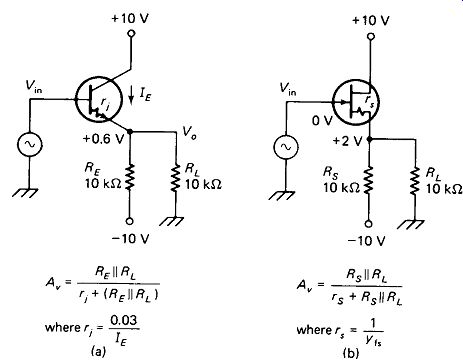
FIGURE 15-5 Emitter followers (a) and source followers (b) have high Z_in, low
Zo, and low distortion.
Av for the source follower also increases on positive signal peaks (for an N-channel FET). This is because y_fs increases at higher ID. The distortion is likely to be more severe with the source follower because rs is generally a much larger value than r_j (250 ohm compared to 32 ohm for the values given in the figure).
Long-tailing is a commonly used technique for minimizing voltage-follower distortion by stabilizing the emitter (or drain) current, thus keeping r, (or rs) constant. In its simplest form, RE (or Rs) of Fig. 15-5 would simply be increased to 100 k-ohm and the negative supply would be raised to - 100 V. The input signal swing (even 10 V p-p) would thus produce a much smaller change in bias current, resulting in less distortion. For long-tailing to be effective, the peak current drawn by RL must be much less than the bias current employed. This means low Vin, high IE, or high RL.
The extra 90 mW lost in the 100-k ohm resistor and the expense of the - 100-V supply are the prices one pays for improved linearity.
Current-source bias is the ultimate in long-tailing, giving, in effect, an infinite Re (or Rs). Figure 15-6(a) shows the technique applied to an FET. R1 and R2 hold 2 V across RJy setting Ic of Q2 at 1 mA regardless of Vc. Again, iRL must be much less than Ic to make this technique effective.
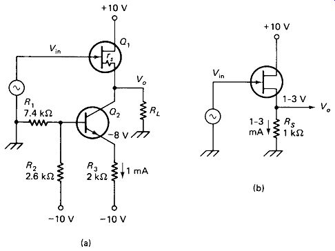
FIGURE 15-6 (a) Current-source Q* stabilizes the bias point and minimizes
distortion due to changing r.. (b) Low voltage across Rs makes the circuit
bias-unstable and increases distortion due to changing r..
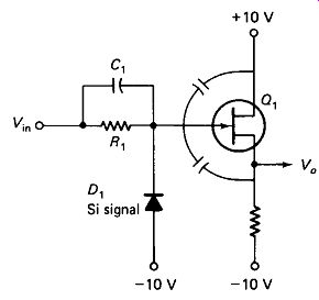
FIGURE 15-7 R1 and D1 protect the gate from accidental overvoltage, but stray
capacitance loads R, at high frequencies. C1 prevents this loading, but nullifies
protection at high frequencies.
Figure 15-6(b) shows a "short tail" source-follower circuit which should be avoided except where V_in is only a few millivolts or where linearity is not essential.
Input Protection against accidentally applied overvoltages is good practice and is exemplified in Fig. 15-7. R, would be calculated to limit the gate current to a safe value (say, 10 mA) for any anticipated positive i should be calculated, as it is apt to be surprisingly high. The FET gate junction will avalanche at typically - 40 V, making even - 10 mA unsafe, so £>, is used to shunt negative overloads to the -10-V supply. For MOSFETs a diode pointing to the + 10-V supply should be added. The diodes should be fast signal types. Power-supply diodes are too slow and have a large capacitance across their junctions.
R1 will drop no voltage at dc and low-frequency ac, since the FET gate and back-biased diode have almost infinite resistance. At some high frequency, however, the FET input capacitance will have a reactance equal to R1 , and serious signal loss (X 0.707) will result. This happens at 88 kHz for Cin = 6 pF and R1 = 300 k-ohm.
C1 is added to prevent this drop, and should be 100 times C_in for 1 % loss, 50Cm for 2% loss, and so on.
It must be understood that the addition of C, nullifies the input protection action at high frequencies, so special care should be taken to guard against high-frequency instrument overloads. TV horizontal sweep circuits, inverter-type power supplies, and radio transmitters are especially dangerous in this respect.
Fortunately, most overloads occur at dc or 60 Hz.
High-Frequency Transients often appear in voltage followers handling sub microsecond pulses. Figure 15-8(a) shows the reason for this problem. When the + 1-V input pulse is first applied, the gate rises by +1 V, but the source (for a few ns) rises by only 0.5 V, because of the voltage division of stray capacitances Cg and C3.
This creates a +0.5-V gate-source signal which demands a rather large increase in ID. Some of this current surge flows back through Cg developing voltage across rs which further increases the voltage at the gate and consequently the drain current demand, in a regenerative effect.
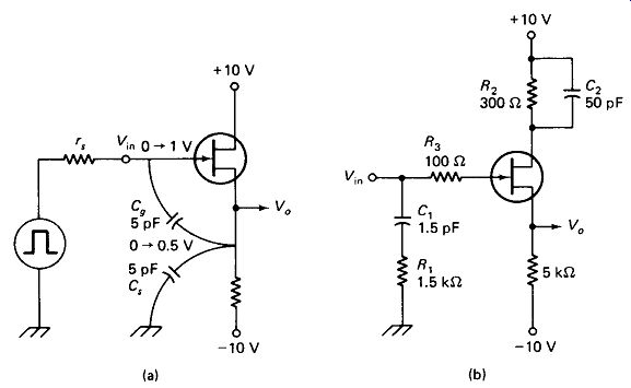
FIGURE 15-8 (a) Voltage division on stray capacitance Cg and C, causes current
surges and ringing on fast-rise pulses, (b) Three techniques for improving
fast pulse response.
The three techniques commonly used to suppress this ringing are shown with typical values in Fig. 15-8(b), although a single circuit is not likely to employ all three at once. R3 limits the rate of rise of gate voltage, and is most effective with amplifiers operating below 10 MHz. C1 and absorb the current fed back through Cg and must be sized to match the stray capacitance Cg. C2 and R2 allow an out-of-phase voltage to be developed at the FET drain. Stray drain-gate capacitance couples this back to the gate, introducing a degeneration to offset the regenerative ringing.
The differential amplifier has properties that make it an excellent counterpart of the voltage follower in producing high-performance amplifiers.
. It responds to dc as well as ac, allowing it to handle transducer-generated signals directly.
. It can be adjusted for zero offset-that is, zero dc out for zero dc in.
. It contains no capacitors or inductors, and can therefore be fabricated easily in IC form.
*Its voltage gain can be varied without upsetting the bias point.
*Temperature, component, and power-supply variations are mostly cancelled by the balanced nature of the circuit.
On the disadvantage side, the dif amp does not have a particularly high input impedance or low output impedance. Also, its output does not appear from one point to ground, but rather between two points, both at a dc level above ground.
This may be an advantage or a disadvantage.
Figure 15-9 shows an FET dif amp with variable gain. Qx is a current source, providing a fixed current through the wiper of R4, which then splits between Q2 and Q3. Any increase in D2 (caused by a positive uln) must therefore be accompanied by an equal decrease in D3 *
If VD2 goes down by 1 V, VD3 will then go up by 1 V. The output signal va is thus formed by mirror-image signals at the two terminals.
Balance: Since may be slightly different for the two FETs, R4 is varied to compensate for the difference. If R4 is set to make va zero when u, n is zero, we are adjusting for zero offset. If R4 is set to make r«-o, we are adjusting for dc balance, a condition wherein the setting of R5 varies the gain but not the zero signal dc output of the amp. To achieve both zero offset and dc balance, the gate of Q3 could be connected to the wiper of a trimpot between ± Vcc.
Notice the balanced nature of the circuit. If + Vcc increases, Voi will increase, but so will V*3- Net va is unchanged. If temperature rises, turning Q2 on more, Q3 will experience an identical change, and again there will be no change in v0.
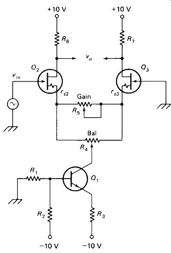
FIGURE 15-9 FET differential amplifier with variable gain.
Gain Calculation: Consider that the right-hand end of r_s3 (Fig. 15-9) is grounded. Also remember that current source Qx presents an infinite resistance, so the wiper of R4 is connected to an open circuit from a signal point of view. Q2 is now a conventional common-source amp, and Av is the ratio of (drain-line resistance)/(source-line resistance), since the same current iD flows in each. The drain line contains only R6. The source line contains r_s2, in series with Rs and R4 in parallel, in series with rs3. The total gain is twice that calculated for Q2, since Q3 makes an equal contribution:
(15-8)
Of course, in most cases R6 = R7 and r_s2 = r_s3.
For dif amps using bipolar transistors, the source resistances rs are replaced with emitter junction resistance rj. We must also be sure that the base of Q2 is fed from a negligibly low impedance [say less than of 1/100 Beta (r_J2 + R4 || Rs + r s3)].
Differential Inputs: Instead of grounding the gate of Q3 (Fig. 15-9) we could have connected one side of the input signal to it, as in Fig. 15-10. The differential amp will now amplify only the difference between the two input gates (V_didf) and will ignore any signals appearing in common between the two inputs and ground (V_com). This is because the FETs split the current from Q1 equally as long as their gate voltages are equal. Raising both gates by 1 V simply results in raising Vcl by 1 V.
Differential inputs are useful in rejecting common-mode noise picked up by the input wires, especially where these wires must be long or are fed by a high-impedance source. As a typical example, Vdlf may be a remote station speaker used as a microphone on an intercom system. The long wires back to the amplifier input pick up considerable noise from the ac line via Cstray, but the noise is picked up in common by both wires. Only the differential signal from the speaker is amplified by the dif amp. Differential amplifiers are used for similar reasons in biomedical sensing and in computer core-memory readout amplifiers.
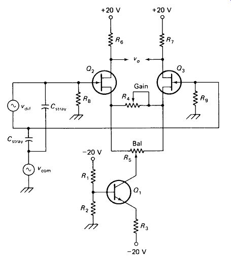
FIGURE 15-10 Dif amp responds to the difference in voltage between two ungrounded
input lines. V_com is rejected.
General-purpose test instruments often have differential inputs so they can monitor the voltage difference between two points, neither one of which is grounded. (Connecting the ground probe of a test instrument to a point other than ground of the circuit under test is generally a poor idea. It shorts the test point to ground if the two devices both have their chassis at ac line ground. Even if the instrument is isolated from the ac line, a great deal of noise will be picked up by the chassis and transformer capacitance to the line, and this noise will then be injected into the circuit under test. Only battery-operated instruments with plastic or isolated cases should have their "common " probe connected to a point other than ground.)
Common-Mode-Rejection Ratio, or CMRR, is the specification detailing how many times more sensitive an instrument is to differential inputs than to common-mode signals. Ideally, the ratio would be infinite, indicating no response at all to common-mode signals, but amplifier and input-attenuator imperfections generally place the ratio between one hundred and several thousand.
To measure CMRR, one input is grounded and an input signal is applied to the other input to produce a certain output (say 1 division deflection on the screen of an oscilloscope). Now the two inputs are tied together and an input is applied in common between both of them and ground, such as to produce the same 1-division deflection. The ratio of the two inputs required is the CMRR.
Common-Mode Voltage Limit: If the voltage applied in common to the gates (Fig. 15-10) becomes too positive, Q2 and Q3 will enter the saturation region and be unable to amplify the differential signal. Also, if the common-mode voltage goes too negative, will saturate and will cease to function as a current source. These two phenomena define the common-mode voltage limits of the amplifier.
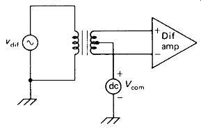
Fig 15-11- Circuit for measuring the common-mode voltage limits of an amp.
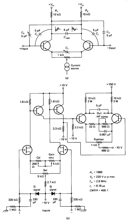
Fig 15-12
Common-mode voltage limits can be measured with the test setup shown in Fig. 15-11. An output reading from Kit is obtained with Vcom at 0 V dc. Vcom is then increased in the positive direction until the accuracy of Km falls out of spec (-3% for a 3%-accuracy instrument). The test is then repeated to determine the maximum tolerable negative V_com.
Frequency Compensation: The collector-junction capacitance of a dif amp may typically be 5 pF to ground. The load may present another 5 pF across the outputs, which appears as 10 pF to ground because of the Miller effect with 2VC across it.
This is illustrated in Fig. 15-12(a). If the collector resistors are 10 k ohm, the Xc will equal R at about 1 MHz, and the output will be loaded down to 0.707 of full output at that frequency. However, a compensating capacitor C, can be placed across the emitter resistance as shown, sized to decrease the emitter line impedance in exact step with the decrease in collector line impedance. The high-frequency limit of the amplifier can generally be extended by a factor of 3 or 4 with this technique. To determine the value of C, required:
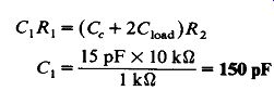
(15-9)
In practice, C, would be adjusted for a high-frequency output (say, 2 MHz) equal to the low-frequency output (say, 1 kHz). A check would then be made to see that no over-peaking was present in the vicinity of 1 MHz. If a waveform can be observed at a later stage, a 200-kHz square wave can be applied and C, adjusted for sharpest response without overshoot. However, no extra loading from scope or meter probes can be tolerated at the collectors of the stage being compensated.
Often C, must exceed 1000 pF, making a variable unit impractical. In this case, C, can be fixed and can be shunted with a variable resistor which is adjusted to achieve compensation. The gain of the amplifier will then be dictated by stray capacitances which are quite unreliable. If an exact overall gain is required, there must be another stage of amplification which is variable without regard to frequency compensation. Variable gain in a compensated dif amp is seldom attempted, because it would require a variable Ct to track with a variable resistance in the emitter.
Input Capacitance: The circuit of Fig. 15-12(a) has a gain of 10 to each collector, so the Miller effect makes the 5-pF junction capacitance from base to collector look like (5 pF) (10 + 1) or 55 pF to ground. This is objectionably high, as it causes low input impedance at high frequencies (2.9 k- ohm at 1 MHz). A common solution is to dive the dif amp with an emitter or source follower, but it is possible to neutralize the input capacitance by feeding an inverted signal to the base from the opposite collector of the differential pair (C2 and C3 in Fig. 15-12). Only C2 is required if the - in terminal is to be kept at ground. C2 should be variable. Variable gain can be employed with no problem.
Figure 15-12(b) shows a complete 3-MHz differential amplifier incorporating the features presented in this section. Voltage gain can be set as high as 1000, with Zin =1 M- ohm, Va - 230 V p-p(max), and Bw = 3 MHz.
15.6 LEVEL SHIFTERS
Differential amplifiers using NPN or N-channel transistors unavoidably have their outputs at a more positive dc level (with respect to ground) than their inputs. Often, we wish to take our output from one of the differential transistors to ground, and it then becomes necessary to shift the dc level of the output back to zero. There are several ways to achieve this:
. Use a zener diode in series with the output to obtain the required level shift. This works well in digital circuits, but avalanche noise and tempera ture drift are objectionable in low-level amplifiers.
. Alternate NPN and PNP stages, letting the NPN' s offset the level in the positive direction and the PNP's return it to zero with their negative offset.
This can be done with discrete components but is usually avoided in integrated circuits because of the difficulty of producing both types of transistors on the same chip.
. Employ a voltage divider to the negative supply, as in Fig. 15-13(a). The loss of voltage gain ( in the example) is not serious, but an emitter follower Q3 is required to reduce loading of the Q2 collector.
. Employ a current source (Q4) and dropping resistor (/?4) as in Fig.
15-13(b). This is similar to the technique of Fig. 15-13(a) except that R5 has been replaced by a current source that has infinite dynamic resistance, so there is no loss in voltage gain.
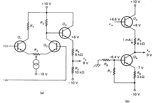
FIGURE 15-13 (a) Voltage-dividing level shifter, (b) Current-source Q< replaces
R3.
15.7 TOTEM-POLE OUTPUT
Single-ended (as opposed to differential) amplifiers and voltage followers have a slower response to fast pulses in the current-decreasing direction than in the current-increasing direction. This is illustrated for an emitter follower in Fig. 15-14(a). This circuit has an active pull-up but a passive pull-down.
The load capacitance CL is charged through the transistor>s collector with a current which may be as large as jiIB. Discharge, however, follows the "negative exponential"
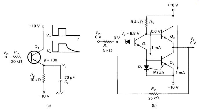
FIGURE 15-14 (a) An emitter follower has active pullup but passive pulldown.
(b) Totem-pole output: Q3 provides active pullup, Q2 provides active pulldown.
Discharge to 5% will take three time constants, which for the values given amounts to 3rdls = 3 X 10 k ohm X 20 pF
= 600 ns
Charge can be accomplished in a shorter time:
= 12 ns since the current through R in is multiplied by fi.
In a dif amp, one transistor's current is increasing while the other's is decreasing, so there is no lack of symmetry. The response time is also not terribly fast if CL is appreciable, which is why the totem-pole circuit of Fig. 15- 14(b) is often used as an output stage. This circuit has active pullup and pulldown, and is similar in many respects to a complementary-symmetry stage.
This circuit uses a current repeater DXQ2 which can be effective only in integrated-circuit form. The base-emitter diode of Q2 is identical to D1, which is only possible since they are on the same chip. They are connected in parallel, so it is certain that they will have the same voltage across them and hence will carry the same current. IEi is therefore equal to IE2 and IE3. If Va attempts to move positive from 0 V, R2 will turn Qt on, which will turn Q2 on, lowering Va
.
If Va drops below
0 V, Qx will turn more off, raising turning Q3 on and raising Va
.
R3 sets the idle currents at 1 mA, and R2/R1 set the gain of the stage at y = 5. Level shifting is required to bring the -8.8 V base of Q, to zero. A zener is shown for simplicity, but one of the methods shown in Fig. 15-13 would be used in practice.
15.8 CHOPPER-STABILIZED AMPLIFIERS
Sometimes it is necessary to amplify dc signals which are so small that they are lost in the dc bias-point drift of even a well-designed differential amplifier. The solution in this case is to chop the input dc into pulses which are then amplified by a simple ac-coupled amplifier and finally detected and filtered back to dc.
If the dc involved is always of one polarity, we can stop at this point, but most often the dc is actually the output of a potentiometer or Bridge circuit and may be of either polarity. In that case we need a detector capable of discerning whether the input signal is positive or negative.
Phase Detector: Figure 15-15(a) represents a dc input signal changing from positive to negative (Vm). Vm is passed when the chopping signal is positive and blocked when it is negative, producing the signal VA. VA is amplified by a capacitor-coupled amp, producing VB. VB is passed when the chopping signal is positive, and blocked when it is negative, producing Va. Va is filtered by a capacitor, reproducing the original transitioning dc waveform.
In practice, the transition would be more likely to take 400 cycles of the chopping signal than the 4 cycles shown, but the principle is the same. The phase of the chopped signal with respect to the chopping signal changes as Via changes from positive to negative, and the detector converts amplified ac of one phase into a positive output while the opposite phase produces negative output.
Choppers and phase detectors have taken many forms: mechanically vibrating contacts, light beams with rotating wheels and photocells, transformers and switching diodes, and others. The FET outperforms most of these devices because it is bilateral (source and drain interchangeable), its gate signal does not inject noise to the source or drain, and it offers solid-state reliability.
Figure 15-15(b) shows a chopper, amplifier, and phase detector employing FETs. Notice that no special biasing or temperature-compensating techniques are employed, yet this system will always produce 0 V out for 0 V in, regardless of power supply and temperature Variations. The chopping frequency of 60 Hz is common because it is readily available and it makes it possible to cancel noise picked up at the line frequency.
The frequency response of a chopper amp ranges from dc to about of the chopping signal frequency, or 6 Hz in the example circuit. The upper frequency can be extended to the megahertz range by shunting the signals above 6 Hz to an ac-coupled amplifier and combining its output with the phase detector's output.
Such a system is properly called a chopper-stabilized amplifier, and has the benefits of high-frequency response and near-zero dc drift.
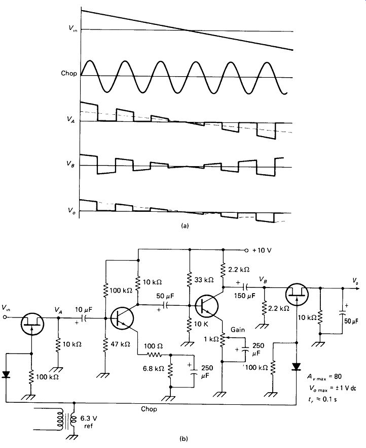
FIGURE 15-15 --- A chopper and phase detector amplifies dc with zero offset and
drift: (a) pertinent waveforms; (b) circuit diagram.