16.1 OP-AMP CHARACTERISTICS
Operational amplifiers were originally developed in vacuum-tube days to perform the mathematical operations of adding, multiplying, and integrating as required in analog computers. The name has stuck but the performance and range of applications for the op amp have grown apace.
There is no strictly accepted definition, but op amps generally have the following characteristics:
. Frequency response from dc to several kHz (although several "fast" op amps operate well into the MHz range).
. Ability to handle both positive and negative dc inputs and outputs.
. Near-zero offset; that is, almost zero input produces zero output voltage.
. Very high voltage gain-typically several tens of thousands.
. High input impedance-typically above 100 k ohm.
. Differential inputs.
Internally, an op amp usually consists of two or three differential-amplifier stages, a level shifter, and a complementary-symmetry or totem-pole output stage. However, there is no need to be concerned with the internals at this point, because most op amps are integrated-circuit devices with no access to the internals.
The symbol for an op amp is given in Fig. 16-l(a). A positive voltage at the inverting input (- symbol) causes the output to swing negative. A positive voltage at the noninverting input (+ symbol) causes the output to go positive. The gain of the op amp is so high that the voltage between the + and - inputs is virtually (very nearly) zero, even for maximum output. This observation forms the basis of much of our analysis of op-amp circuits. Notice that two power supplies are required for the op amp, one positive and one negative with respect to ground.
These supply connections are often omitted in circuit diagrams, but of course they cannot be overlooked in wiring the circuit.
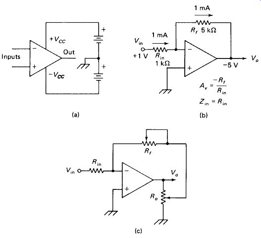
FIGURE 16-1 (a) Op-amp symbol and power-supply connections, (b) Basic Inverting
op-amp circuit with example values for gain of -5. (c) Two methods of varying
circuit gain.
16.2 THE INVERTING OP-AMP CIRCUIT
The most popular op-amp circuit is the inverting amplifier of Fig. 16-1(b). The gain of this circuit is controlled by the ratio of Rf/Rin and is almost completely unaffected by internal op-amp gain, supply voltage, or temperature. The example numbers given with the figure illustrate why this is true. The + 1 V at ViB will bring the - input positive, forcing the output negative. The negative output will force a current through Rf in the direction shown. Now it is important to remember that the voltage and current at the - input are virtually zero. (For 5 V out and Ac = 10, 000, Vm = 5/10,000 = 0.5 mV. The input current, for an rm of 1 M ohm would be 0.5 mV/1 M- ohm, or 0.5 nA.) Therefore, I_Rm is virtually equal to I_Rf and the junction of Ria and Rf is virtually at ground potential. The only V0 that will produce the required 1 mA in is - 5 V. A less-negative VQ would immediately route more of the R_in current to the - input, making Va more negative.
The Input Impedance for this circuit is equal to R_in, since the right-hand end of R_in is virtual ground. Rf can be a variable or a photosensitive resistor, making Av variable. Values of Rj above 1 M-ohm generally require special op amps or offset-adjust circuits to keep the output at zero for zero input. Figure 16-1(c) shows two methods of gain control for the inverting op-amp circuit.
16.3 THE NONINVERTING OP-AMP CIRCUIT
The noninverting circuit has a much higher input impedance than the inverting circuit, but it requires the input signal to appear as a common-mode voltage on the + and - inputs. This means that common-mode voltage limit and input stray capacitance present problems which do not appear in the inverting circuit where both inputs are kept near ground. The noninverting circuit is therefore less easy to tame than the inverting circuit.
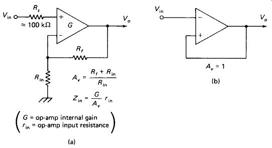
FIGURE 16-2 (a) The noninverting circuit gives much higher input impedance
than the inverting circuit, (b) Gain-of-one voltage follower.
Figure 16-2(a) shows the noninverting circuit and its gain and input-resistance equations. Rf and Ri form a voltage divider applying a fraction of VQ back to the - input. The voltage between + in and - in is virtually zero, so this fraction must equal Vin.
Rs is not essential, but is recommended to protect the op amp where overvoltages could be applied to the input. Figure 16-2(b) shows a unity-gain voltage follower, which is really just a special case of the noninverting circuit with Rf= 0 and Rin --> oo.
16.4 OFFSET VOLTAGE--CAUSES AND CURES
An ideal op amp would have zero output voltage with zero input voltage and zero input current. In practice, zero input will cause the output to offset (assume some nonzero value) in order to feed back a current and voltage to the - input through Rf as required by input-stage imperfections. This output-voltage offset can be minimized by keeping the value of Rj low, but there are several other methods available.
Input Bias Current is the current required by the bases of the differential-input transistors within the op amp. This current is assumed to be 1 uA for each input in the gain-of-10 circuit of Fig. 16-3(a), although modern op amps are available with bias currents tens and even hundreds of times less than this. Notice that, with the input grounded, + 1 V is required at the output to supply 1 uA through Rf to the - input. The current through R in is zero since the - input is virtually ground.
The 1uA to the + input comes from ground but causes no voltage drop, since there is no resistance in this line.
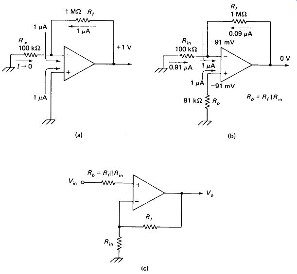
FIGURE 16-3 (a) Input bias current requirements force the output to assume
a nonzero value even when the input is zero, (b) Bias-compensating resistor
R_b minimizes output offset, (c) Placement of R_b in noninverting circuit.
The + 1-V output-voltage offset could be reduced by decreasing Rf, but this would require a corresponding decrease of R , resulting in lower input impedance.
An op amp with lower bias current could be used, and indeed low-cost/low-speed op amps are available with bias currents on the order of 10 uA, and at a higher price 1 uA is obtainable. High-speed op amps generally have higher bias-current requirements, however.
Figure 16-3(b) shows how a bias-compensating resistor Rb can be added at the + input to eliminate output offset if the input bias currents are equal. The - input bias current is obtained through Rin and Rf, which are in parallel if Vo = 0 and Vm is grounded. Rb is chosen equal to Rin || Ry, so the voltage developed at the - input (across in||/?y) equals the voltage developed at the + input (across Rb).
The differential-input voltage is then virtually zero. The value of Rin in this determination includes the resistance of the signal source if it is not negligible.
For the noninverting circuit, bias compensation requires that the input protection resistor Rs assume the function of Rb, and have a value /?m || R , as shown in Fig. 16-3(c). Here Rb includes the resistance of the signal source.
Input Offset Current: The + and - input transistors of an IC op amp are fabricated on the same chip, so their bias-current requirements tend to be equal. To the extent that they are not equal, the compensating resistor Rb will be ineffective in eliminating output offset. The difference between the input bias currents is called input offset current, and is typically 1/10 to 1/3 of bias current for most op amps.
Some op amps have a terminal or pair of terminals provided for connection of an offset null pot, in which case the manufacturer's recommendation should be followed. If no such provision is made, the circuit of Fig. 16-4(a) can be employed. The bias-current-compensating resistor Rb is still recommended, even though R and R_null could supply all the bias required by the - input. This is because the bias currents change with temperature, and the setting required of R null would therefore change with temperature. However, the bias current changes do tend to track with temperature, so the inclusion of Rb makes output offset less sensitive to temperature changes.
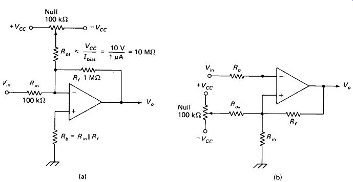
FIGURE 19-4 Offset current is the difference between the two input bias currents.
Offset null circuits for inverting (a) and noninverting (b) amps are shown.
The null circuit for the noninverting op amp is shown in Fig. 16-4(b). Note that in this case R_os is effectively in shunt with R m, and the circuit gain will be increased if Ros is not many times larger than R .
Input Offset Voltage is the voltage difference that must be applied between the two inputs of an op amp to force its output to go to zero. Ideally, both transistors of the input dif amp would turn on at the same voltage, but slight differences do exist. Input offset voltage is specified at 0.5 to 10 mV for commonly available op amps. In Fig. 16-5(a), input offset voltage is represented as a voltage source in series with the + input in an inverting gain-of-10 circuit. Notice that the output voltage must assume a value V_os (Av + 1) in order to bring the ideal + and - inputs to zero differential voltage. (Bias and offset currents are being neglected for the moment.) Decreasing Rf and Rin will not reduce the output offset due to Vos as it will in the case of I_bias and I_os.
Offset voltage is usually the predominant problem in high-gain circuits, whereas offset current tends to predominate in high-impedance circuits.
Figure 16-5(b) shows a circuit designed specifically to null out input offset voltage in an inverting op amp. Of course, the current null circuit can be used to take care of voltage and current offset in one adjustment. It is not common practice to include both null circuits because it is very difficult to monitor the actual input offsets, and both controls affect the output offset in the same way. An exception to this may occur when gain is variable and the source resistance rs varies widely. The offset voltage control would first be used to null the output with rs at minimum (input grounded). Then the offset current control would be adjusted for ...
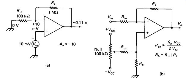
FIGURE 16-5 (a) Input offset voltage also causes output offset, (b) Input
offset voltage null circuit.
... zero output with rs at maximum. Repeating these two steps, a point should be reached where zero input voltage produces zero output voltage regardless of gain setting or input-resistance conditions.
HIGH-FREQUENCY EFFECTS
Feedback and Oscillation: When used as linear amplifiers, op amps are connected with negative (or 180 °) feedback from output to inverting input. At high frequencies, additional lagging phase shifts are developed as the collector resistance of one stage feeds the base capacitance of the following stage. At some frequency, this internal phase shift will total 180°, resulting in a total phase shift of 360° in the fed-back signal. If the amplifier gain at this frequency is sufficient to make the fed-back signal equal the input signal, the signal will regenerate, and the amplifier will self-oscillate. To prevent this from happening, it is necessary to reduce the high-frequency gain of the amplifier so that the fed-back signal will not be sufficient to regenerate the input signal. This is accomplished by negative feedback or signal shunting of high frequencies through small-value capacitors or RC networks. This is termed frequency compensation.
External Frequency-Compensation
Components are added according to manufacturers' data sheets and application notes, since each op amp has its own requirements. In general, low-/!,, circuits have large amounts of feedback (low Rf) and consequently require greater attenuation of high-frequency gain to preserve stability. Too little compensation will produce ringing on square-wave edges and oscillation if it is severe. Too much compensation will simply lower the upper frequency limit of the amplifier. Figure 16-6 (a) and (b) shows the compensating components and resulting frequency response for the type 709 op amp. Notice that curve 1 compensation will provide a gain-of-100 amplifier, but the upper frequency ...
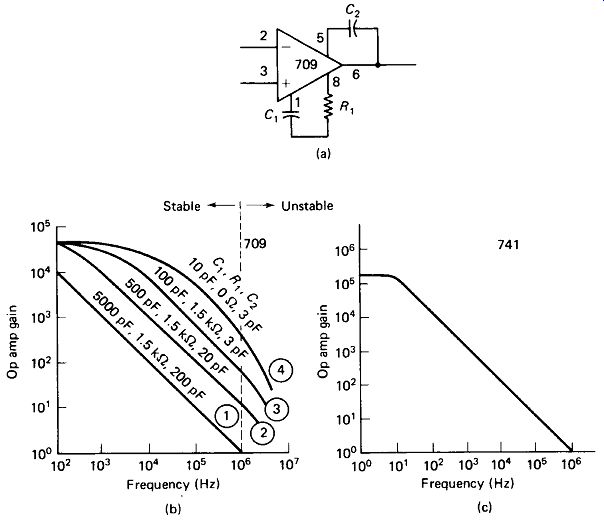
FIGURE 16-6--- Frequency compensation is required to prevent oscillation in
op-amp amplifiers: (a) compensation components for the 709 op amp; (b) open-loop
gain versus frequency for the compensated 709; (c) open-loop gain drops off
rapidly at high frequencies for the internally compensated 741.
... limit will be only 10 kHz. Curve 2 compensation will permit a gain of 100 with a 100-kHz bandwidth. However if curve 2 compensation is used on a gain-of-3 amplifier, oscillation would be the certain result.
Internal Compensation relieves' the user of the burden of selecting compensating components. The compensating capacitor is integrated on the chip and sized for the heaviest feedback possible, which is a unity-gain circuit. Such fixed compensation allows maximum frequency response only at unity gain. For higher gains frequency response is reduced proportionally. Figure 16-6(c) shows frequency response versus gain for the 741 op amp.
Feed-Forward Compensation is a technique of shunting high frequencies around a relatively slow stage of an op amp through an external capacitor of a few hundred picofarads. Frequency response can be improved by as much as a factor of 10 in op amps with this option. Feed forward is applicable only to the inverting circuit.
Slew Rate is the maximum rate of change in output voltage (expressed in V//xs) in response to a much-faster-rising input step. This parameter may impose its limitation at a much lower frequency than the frequency-response curves would indicate if the output signal is large. For example, the curve of Fig. 16-6(c) indicates that the 741 op amp should have an upper frequency limit of 100 kHz in a gain-of-10 circuit. However, the slew-rate spec is only 0.3 V//xs, which, as Fig. 16-7 shows, implies a frequency limit of 15 kHz for a 10-V-p-p output sine wave. Slew rate is generally measured in the voltage-follower circuit of Fig. 16-2(b), which is the worst-case condition.
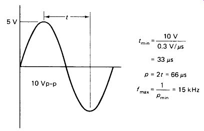
FIGURE 16-7 Slew-rate limitations cause large voltages to be attenuated at
lower frequencies than small voltages.
16.6 OP-AMP APPLICATIONS
FET Inputs: Instrumentation circuits sometimes require a dc-responding amplifier with a near-infinite input impedance and low offset regardless of source resistance. The FET-input op amp in a noninverting circuit fills the requirement nicely. Bias current for the 536 op amp (sometimes called a Bi-FET because of its combination of bipolar and FET circuitry) is specified at 30 pA, maximum. Input offset voltage for the Bi-FETs is several times greater than for bipolar inputs, but this is easily nulled out. Figure 16-8(a) shows the low output offset resulting when a Bi-FET op amp is driven from a high-impedance source. Even the best bipolar inputs will produce offsets 100 times as great.
Figure 16-8(b) shows how a pair of discrete FETs can be used to obtain some of this advantage with a conventional op amp.
The circuit is noninverting, with the feedback returned to the FET input. The FETs are differential source followers, with the NULL pot making up for differences in VGS.
The FETs should be matched for VGS(oU) and thermally bonded together, or if available, should be a matched pair in a single package.
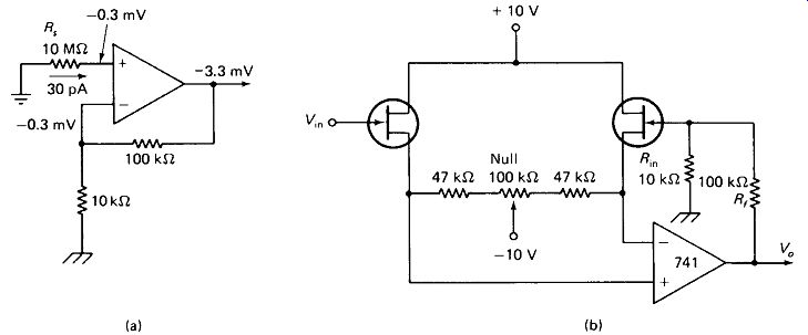
FIGURE 16-8 (a) Bi-FET op amps have extremely low bias currents and can be
driven from high-impedance sources without serious offset, (b) FET inputs can
be added to a conventional op amp.
Power Output: Most op-amps have a total power-dissipation limit of 500 mW and will operate from supply voltages from ±5 to ± 18 V. 50-W op amps with 1-A output currents are available, but power output can be realized with a low-power op amp driving a complementary-symmetry output stage, as shown in Fig. 16-9.
Notice that the feedback is taken from the transistor outputs, and not from the op amp directly. The first circuit requires the op-amp output to swing to +0.6 and -0.6 V before the NPN and PNP transistors, respectively, begin to turn on, and crossover distortion will be noticeable at higher frequencies. The added resistors in the second circuit bias the transistors at the threshold of conduction, eliminating crossover distortion. The inverting circuit is shown in the example, but the noninverting circuit can be used as well.
Some op amps are inclined to be unstable if their power-supply lines are not clean. The 10-ohm resistors and 0.1-uF capacitor shown in Fig. 16-9(b) filter the supplies before they reach the op amp, ensuring stability.
Single-Supply Operation: Sometimes it is desirable to utilize an op amp in a system that does not have positive and negative supplies. Figure 16-10 shows how this can be done for noninverting and inverting circuits. Ac coupling is mandatory in these single-supply circuits unless Vm is reliably positioned between Vcc and ground.
Differential Inputs: Where neither of the input signal wires is grounded, or where it is desired to amplify the difference between two signals (both referenced to ground), or where two signals are to be subtracted, the differential op-amp circuit of Fig. 16-11(a) may be used. Sample resistance values and input voltages are given as an aid to understanding the circuit operation. The noninverting R_in and R_f resistors form a simple voltage divider, since the + op-amp input has very high Z_in.
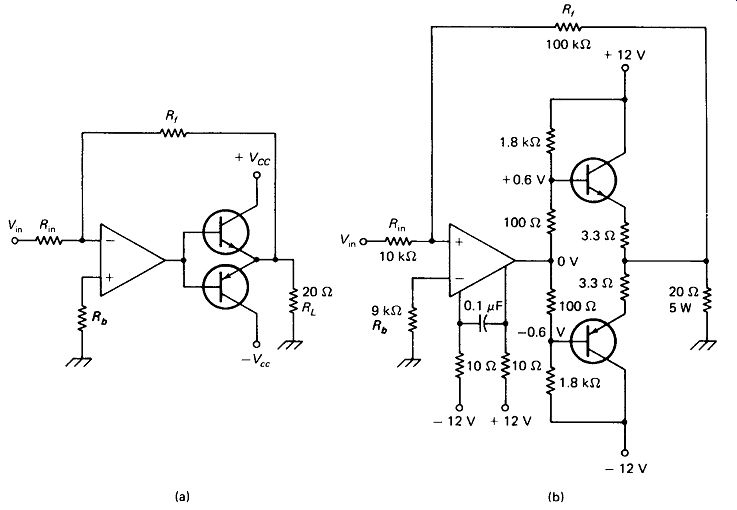
FIGURE 16-9 Complementary-symmetry power-output stages for op amps: (a) simple;
(b) biased and supply-decoupled for minimum high-frequency distortion.
The rest of the voltages follow directly from the fact that the voltage between the + and - inputs is virtually zero.
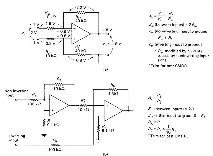
Figure 16-11.
The common-mode rejection of this dif amp depends upon the degree of matching of the two Rj/Rm ratios, so precision resistors or a trimmer in series with the grounded Rf should be used if high CMRR is desired. The common-mode input voltage should be limited to about half the supplies with this circuit.
The impedance at the inverting input is lower than at the noninverting input, and signals at the noninverting input will cause currents in the inverting input line.
It is therefore advisable to drive the circuit of Fig. 16-11(a) through a pair of voltage followers [Fig. 16-2(b)] unless the source impedance to ground is several hundred times lower than R_in.
Figure 16-11(b) shows a differential op-amp circuit with identical Z_in at each input and a common-mode voltage range of almost 10 times the Vcc supplies.