17.1 IMPEDANCE MATCHING
When a signal source with a source resistance Rs is used to drive a load RL, it can be shown that maximum power is delivered to the load when RL = Rs.
This was illustrated in Fig. 5-4. Lower values of RL increase load current, but decrease load voltage, resulting in less load power. Higher values of RL increase load voltage, but decrease load current, also resulting in less load power. This is one reason for matching the speaker impedance (4, 8, or 16 ohm) to the amplifier output impedance in an audio system. The effect should not be overestimated, however. Notice from Fig. 5-4 that a 2 : 1 mismatch causes only an 11% power loss.
Several other factors concerning impedance matching should be kept in mind:
. At match, the power wasted in the source resistance equals that delivered to the load. In drawing power from a battery we would prefer not to match but to keep RL much greater than Rs to conserve energy. Mismatching with RL too high is often preferable to having RL too low for this reason.
. In driving a bipolar transistor amplifier, the input current is what operates the transistor. Designing an amplifier for 10 k ohm Z_in because it is to be driven by a 10-k ohm R_s microphone is therefore an error. Zin should be kept low to maximize input current.
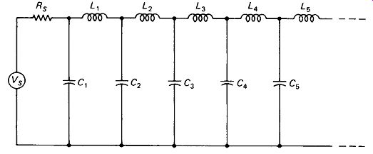
FIGURE 17-1 A transmission line can be represented as a series of infinitely
small capacitors and inductors.
. In driving an FET or vacuum tube, the input voltage operates the amplifier, and Zin should be kept many times higher than Rs to maximize V_in.
Attempts to maximize P_in are misdirected.
17.2 TRANSMISSION LINES AND REFLECTIONS
A more compelling reason for matching RL to Rs appears when high-frequency signals are sent over long transmission lines (i.e., when the line is longer than about wavelength at the frequency in use). The lengths involved are about 30 km (20 mi) at audio frequencies, 30 m (100 ft) at 1 MHz, and 0.3 m (1 ft) at 100 MHz. To understand the effect we must first look closely at a transmission line.
Characteristic Impedance of a Line: Figure 17-1 represents an infinitely long transmission line. The stray capacitance from the center conductor to the shield is represented by the series of small capacitors C. The inductance of the center conductor is represented by the series of coils L.
If a dc voltage is suddenly applied by Vs, C, will initially accept a charging current through Rs, and L, will initially block current from the rest of the line. As C, finishes charging, L, will begin to pass current to C2 and L2 will block current from the rest of the line. This process continues indefinitely, with Vs supplying a constant current Is, the energy being used to charge the infinite series of L and C components. The effect (a constant voltage producing a constant current) is exactly the same as if the infinite line were a resistance, Ra = Vs/Is.
The value of this effective resistance Ra depends upon the physical structure of the line. It is lower for lines with thick conductors closely spaced, because this makes the C values larger, increasing Is. Thin conductors increase L, tending to decrease Is and raise Ra.
Ra is termed the surge resistance of the line, and is the same as Za, the characteristic impedance of the line. Za can be shown by network analysis of the reactance of the L and C components to be given by the equation:
(17-1)
… where L and C are the inductance and capacitance, respectively, per unit length of line. Note that Za is purely resistive for an infinite line.
EXAMPLE 17-1
What is the characteristic impedance of a line having an inductance of 0.2 uH/m and a capacitance of 50 pF/m?
Solution Terminated Lines: Infinite lines, of course, do not exist, but if a long section of line is terminated by a resistance equal to Z0,
the line behaves as if it were infinitely long. This is true because an infinitely long line looks like a resistance of value Ra. The resistance, absorbing energy and dissipating it as heat, cannot be distinguished (from the vantage point of the source) from an infinite line storing the energy in its infinite series of L and C components.
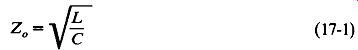
Reflections from an Open Line: If a short pulse is applied to a finite transmission line that is unterminated at the far end, the incident (outgoing) energy will have no place to go-no resistance to dissipate it, and no further LC components to pass it on to. The end capacitance of the line will then simply discharge itself back through the inductance that charged it, reflecting the pulse from the end of the line back to the source.
This is a most interesting experiment that can actually be performed if a fairly fast scope and pulse generator are available. The setup is shown in Fig. 17-2. For a 10-MHz scope the line should be about 100 m (300 ft) long, and the pulse generator should be set for 0.1 -/ns-wide pulses at about 200 kHz repetition rate. For a faster scope the line can be shortened and the pulses speeded up proportionally if desired.
The impedance of the generator must equal the Zc of the line used, or the two ends of the line will play ping-pong with the signal, making the first reflection difficult to see. Since most pulse generators have Rs = 50-ohm, this means adding 250 B in series with the pulse generator for 300-ohm TV twin lead, or 25 ohm for 75-ohm coax cable.
The oscilloscope will display the incident pulse with the reflected pulse following by a time calculated as where d is the length of the line (the factor of 2 indicates that the pulse travels out and back) and vp is the propagation velocity of a signal on the line. This is typically ...
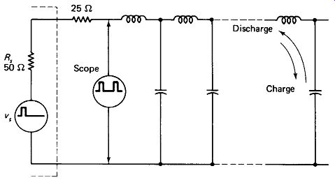
FIGURE 17-2 An open-end transmission line reflects an upright signal back
to the source.
... 200 x 10f m/s for 50- and 75-ohm coax and 250 X 10f m/s for 300- ohm twin lead.
Special open-wire lines with ceramic spacers may have v of 290 X 10f m/s.
Once v for a given type of cable is known, a measurement of t gives distance d to a break in the cable directly from equation 17-2. This technique, called time-domain reflectometry (TDR), is of tremendous value in locating faults in underground and undersea cables.
Reflections from a Shorted Line: Figure 17-3 shows a pulse applied to a transmission line which is shorted at the far end. In this case the inductance at the end of the line is caught with no place to send its stored energy, so it discharges into the line that fed it. This inductive kickback is opposite in polarity from the incident pulse, so the reflected pulse is inverted.
FIGURE 17-3 A shorted-end transmission line reflects an inverted signal back
to the source.
The amplitude of the reflected pulse will equal that of the incident pulse if the line is lossless and the termination is a perfect short (or open) circuit. Any termination that is not equal to Z0 will produce some reflections from the termination point which become larger in amplitude as the termination resistance strays away from Ze and nearer a short or open circuit. In particular, the fraction of voltage reflected is given by a reflection coefficient (gamma):
(17-3)
... where Vr is reflected voltage, Vi is incident voltage, RL is the load or terminating resistance, and Z0 is the characteristic impedance of the line.
It might be wise to emphasize here that the discrete or lumped L and C components represented above are actually distributed along the line. The actual representation of even a finite length of line would have to contain an infinitely large number of infinitely small L and C components. Analysis of the LC network on a lumped value per meter (or per foot) would indicate pulse-shape distortions and high-frequency limits which are not present in the real distributed-component line.
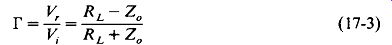
17.3 STANDING WAVES
Let's watch a movie of a 100-V-pk sine wave being applied at the start of the positive half-cycle to a line that is one wavelength long. The line is terminated in a resistance higher than Za.
Let us say that Zc
= 100 ohm and RL
= 300 ohm,
so that 50% of Vi is reflected (noninverted) as Vr.
A frame of the movie is shown each quarter-cycle in Fig. 17-4. The first four frames show the positive wavefront approaching the end of the line (right) as the source (left) goes through a full + then - cycle and gets ready to go + again.
The fifth frame (1 -cycle) shows the half-amplitude positive reflected wave front (dashed line) headed back from the end of the line. The subsequent frames show the incident wave advancing to the right a quarter-wavelength each frame, while the reflected wave advances \ to the left each frame. The heavy line shows the sum of and Vr, which is the voltage that would actually be observed at each point on the line at each instant pictured.
Consider that you are monitoring the voltage at the \ \ point on the line. As the cycle progresses you will measure 0 V, + 100 V, 0 V, - 100 V, and of course, all the values that the sine wave assumes between these quarter-cycle points. The same is true of any other point on the line in the absence of reflections.
Once the reflected voltage begins combining with the incident voltage, however, the waveforms observed at various points on the line are not identical. At the | \ point, for example, the voltage passes from 0 V at 1 \ cycles to - 50 V, to 0 V, to + 50 V. The reflected wave always subtracts from the incident wave, producing a peak voltage of only 50 V.
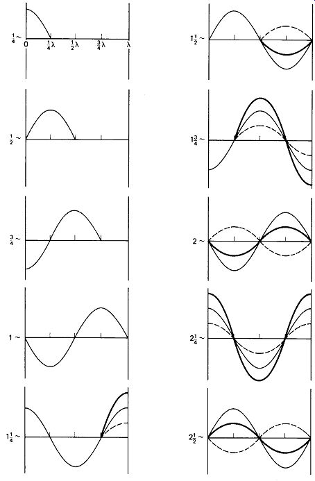
Fig. 17-4
At the j A point the reflected wave always adds to the incident wave, yielding a 150-V peak. At X the wave is 50 V pk, and at 0 X it is back to 150 V pk again.
These voltage nodes and crests always appear at multiples of | A from the point of reflection. They are stationary, or appear to stand in one place, hence the term standing waves.
The ratio between the voltages at the crest and node is called the standing-wave ratio (SWR) or voltage standing-wave ratio (VSWR). Current standing-wave ratio ISWR is numerically identical. In our example, the SWR is 150 V/50 V, or 3: 1.
The current on a line is a maximum at the point where the voltage is minimum, and vice versa. In this case IL = Vrl/R1 = 150 V/300 ohm = 0.5 A. The ratio of currents is the same as the ratio of voltages so the current peak is 0.5 A X 3 = 1.5 A.
Interestingly enough, SWR can be calculated as simply the ratio of impedance mismatch:
Z R SWR = -- or SWR = - (17-4)
It must be emphasized that this entire discussion has been based on resistive not reactive-loads. The phase shifts and impedance transformations that result when the load impedance is partly reactive can be predicted with the aid of a great little toy called the Smith chart, but we haven’t room to go into that here.
17.4 WHAT'S WRONG WITH STANDING WAVES?
We started the investigation of reflections and standing waves with warnings about " compelling reasons " for avoiding impedance mismatch. We now list some of the reasons.
Smear and Ghosting in TV Pictures: If a TV antenna line is longer than about 24 m (80 ft), reflections on the line will cause a second picture /xs or more later than the first. This begins to be a noticeable fraction of the 63-u-s horizontal sweep time, so the second picture produces a smear along the edge of the picture details. Where the lines are 10 times this long the second picture will be displaced 1 or 2 cm to the right of the first-the familiar TV ghost. (Ghosts on TVs with short antenna lead-ins are caused by reflections of the radiated signal from buildings or other objects along the transmission path, not by line reflections.)
Reflected Power is lost to the load, but is added to the signal source. Consider the following example:
EXAMPLE 17-2
A source delivers 100 V rms to a 100-A line terminated in 100 ohm. How much power is delivered to the load? The load changes to 300 ohm. How much power is delivered, and what is the effect upon the source dissipation?
FIGURE 17-5 (a) Standing waves mean reflected power which is dissipated in
the transmitter, (b) Standing waves cause feed-point impedance to vary with
length of line, (c) Shorted or open stubs of line can be used as tuned circuits
or traps. Feed point Z varies Stub tuning
Solution
In the matched case, where SWR =1:1, the line is said to be flat and load power is calculated directly:
If R L is changed to 300 ohm, reflection coefficient is T Rl-Zq 300- 100 RL + Z0 =300+ 100
The load voltage is the 100 V incident plus the 50 V reflected:
The reflected voltage produces an added power in the source which depends upon the source impedance and whether it is reactive or purely resistive, and upon the length of the feedline which affects the relative phase of the incident and reflected voltages across the source resistance.
Radio transmitters using class C output stages are often designed to dissipate only 30 W while outputting 100 W, so any significant added power due to reflection back to the source could prove disastrous.
Feed-Point Impedance Varies with the length of the transmission line if there is a mismatch at the end. In Fig. 17-4, for example, the impedance seen by the source driving the line at 0A is R = V/I = 150 V/0.5 A = 300 ohm. This is equal to the load R1, and the same impedance would be seen if the first 1/2 lambda of the line were cut off and the remainder driven from the 1/2 lambda point. In general, the impedance1/2 lambda or any multiple thereof from a load RL equals RL, no matter what the Za of the line.
In the same figure the impedance seen if the line were driven at the 1/4 lambda or 3/4 lambda point would be R = V/I = 50 V/1.5 A = 33 ohm. In general, the impedance £ A or any odd multiple thereof from a load RL equals Z^2 /RL.
The range of impedances that might be presented to the driving source, just by pruning the transmission line is, in this case, 9 : 1. In general, the maximum and minimum possible impedances presented by a transmission line are in the ratio of SWR2.
This is not all bad. Intelligently cut lines make very efficient and low-cost impedance transformers. Quarter-wavelength stubs of line left open at the end present zero impedance at the frequency for which they are A, making very effective null or trap filters. In a similar manner, quarter-wave stubs with shorted ends or half-wave stubs with open ends make excellent tuned circuits. More often than not, however, we would prefer to keep the transmission line flat (1:1 SWR), so its length can be varied to suit the physical requirements without worry about electrical consequences.
Voltage and Current Peaks on a high-SWR line can waste power due to excessive I^2 R loss and overheat the cable in high-power applications. Dielectric breakdown often appears first at a voltage crest, caused by a higher-than-expected SWR.
17.5 THE L PAD
The L pad is a simple series-resistor voltage divider, so named because it can be (but usually is not) drawn in the shape of a letter L. If one has plenty of signal to spare, an L pad can be used to stabilize the output impedance of an unruly signal generator, as shown in Fig. 17-6(a). For the values given in the figure, Za varies only from 48.6 to 48.9 ohm, even though the actual generator impedance varies from 20 to 200 ohm. The price paid for this stability is an output reduction from 10 V to about 0.4 V.
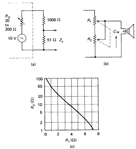
FIGURE 17-6 (a) An L pad makes the generator source Impedance Z_o relatively
constant even though R_G varies, (b) Ganged linear and log pots form an L pad
which maintains a constant Rln while adjusting speaker volume, (c) Chart showing
required values of R1 and R 2 in (b).
L pads are often used as remote-speaker volume controls in an attempt to keep the total impedance constant. The objective is usually to keep an adjustment of one speaker from changing the volume at another speaker elsewhere in the system. The arrangement for an 8-i speaker consists of a linear 8-ohm pot R1 ganged with a log-taper 50 ohm pot R2, as shown in Fig. 17-6(b). The required values of R1 and R2, shown in Fig. 17-6(c), seldom track exactly, but perfection is not required.
Frequency-Compensated Attenuator: Voltage-divider attenuators are very widely used to select the range of all types of voltmeters and oscilloscopes. These instruments have input resistances standardized at 1 M- ohm or 10 M ohm. Each resistor in the voltage divider can be expected to have a stray capacitance of at least 2 pF across it, due to its own structure, wiring, and switch capacitance. Two picofarads has a reactance of 10 M ohm at 8 kHz, making a 10-M ohmresistive voltage divider completely useless at that frequency. Even at 1 kHz the error caused by the capacitance could approach 1%.
High-impedance voltage dividers, even for moderate frequencies, are always compensated with trimmer capacitors, as shown in Fig. 17-7(a). The ratio of resistances RA/RB is equal to the ratio of capacitive reactances, XCA/XCB.
Another way of expressing this relationship is
RaCa = RbCb = RtCt (17-5)
The input capacitance of the instrument (10 pF) and the stray capacitances associated with RA and RB simply appear in parallel with and become part of CA and CB. The input resistance of the instrument is usually infinite since the input amp contains an FET.
FIGURE 17-7 (a) 1 /10 attenuator with compensation for stray capacitance,
(b) Two attenuator sections and an amplifier input designed for mixing and
cascading.
An oscilloscope with ranges from 5 mV/division to 20 V/division in a 1-2-5 sequence would require eleven attenuators of the type shown in Fig. 17-7(a).
Furthermore, there would be no assurance that the input capacitance would be the same on each range, since each CA would be adjusted to compensate for variations in CB and various stray capacitances. In practice, four standard input attenuators are used for this job. Figure 17-7(b) gives an abbreviated illustration of how the attenuators are used in cascade.
Each attenuator is designed to present a 1 M ohm || 20 pF load to whatever drives it, and in turn to drive a 1 M ohm || 20 pF load. Capacitors Cc are added to each attenuator and the input amp to bring the capacitance up to 20 pF. Resistors RB are sized to make the required voltage division when shunted by the 1-M ohm load of the following attenuator. Table 17-1 shows the attenuators used on each range.
Table 17-1
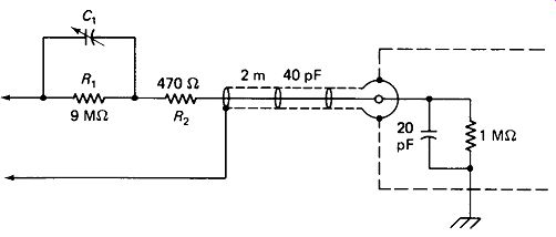
FIGURE 17-8 A x 10 oscilloscope probe. The signal Is divided by 10; the scope
scale factor Is multiplied by 10.
External low-capacitance probes are often used on oscilloscopes to reduce the loading that appears at high frequencies when the entire input capacitance of the scope (20 to 50 pF) plus the shielded cable (20 to 60 pF/m) is connected across the circuit under test. Figure 17-8 shows a typical X 10-attenuating-probe circuit.
The probe reduces the capacitive loading from a 60-pF shunt to 6.7 pF in series with 60 pF or a 6-pF shunt. The resistive loading is reduced from a 1-M ohm shunt to a 10-M-ohm shunt. The price for this is reduced sensitivity. The 5-mV/division scale becomes the 50-mV/division scale using the probe.
The cable used in probe applications has a very thin center conductor to minimize capacitance. It therefore has a characteristic impedance of several hundred ohms, but the 1-M-ohm termination presented by the scope is still an open circuit by comparison. Nor does R1 present a proper termination for the reflected signal on its way back. A series of reflections back and forth along the cable must therefore be expected. /?2 is chosen to dissipate the energy of the reflections, although it is negligible in the voltage-division process. On a 2-m line the reflections will be about 15 ns apart. A 10-MHz scope has a rise time of 0.35/10 MHz - 35 ns, so the first several reflections would not be noticed. Very fast scopes require more sophisticated probes and signal-acquisition techniques.
17.6 SYMMETRICAL ATTENUATORS
Simple resistive networks can be designed which voltage-divide an input signal by a desired ratio while presenting a resistance equal to Za when viewed from either the source or the load. This is assuming that Rs = Za and RL = Za
.These devices have several advantages over the L pad.
. The input and output are interchangeable. They can be inserted in the line either way, and signals sent over the line in either direction will experience the same loss.
. They preserve a constant line impedance, thus eliminating the problems associated with reflected signals.
. They tend to " cover up " for faults in Zs and/or Z0.
A shorted or open load seen through a symmetrical attenuator will look like a resistance rather near Za regardless of the load fault. This effect is called padding and is more pronounced for high-attenuation pads.
Remember, however, that attenuators are essentially power wasters-they are generally used only in low-level applications where the signal source is stronger than required.
The Pi Pad, with its design and analysis equations, is shown in Fig. 17-9. It is essentially a voltage divider shunted by a resistor to keep the input resistance down to Z_o. RL is shunted directly across the output of the pad and forms part of the voltage-divider circuit. It is assumed that RL = Z_o and other values of RL will upset the attenuation ratio. This problem is less severe for higher attenuation factors.
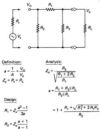
FIGURE 17-9 (pi) attenuator with design and analysis formulas.
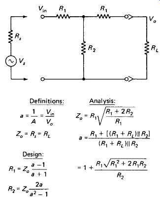
FIGURE 17-10 T (tee) attenuator with de sign and analysis formulas.
The T Pad appears with relevant equations in Fig. 17-10. It is simply an alternative to the pi pad and provides identical performance.
FIGURE 17-11 (a) Padding a line at intervals minimizes reflections from the end in case of a break, (b) Input impedance presented by a pad with an open-circuited load side, as a function of pad attenuation.
Padding to preserve line impedance is illustrated in Fig. 17-11. If a break should occur in the line between tap-off boxes B and C, the remaining stub of line would send unwanted reflections back to boxes A and B and may form a tuned stub trapping out certain frequencies at boxes A and B. Pads placed at regular intervals along the line will preserve a relatively constant impedance along the intact portion of the line, keeping these customers in good service until the break is repaired. The graph given with the figure shows the impedance seen looking into the pad for an open-circuit load for various values of pad attenuation.
EXAMPLE 17-3 A T pad has Rx = 22 ohm and R2 = 100 ohm. Find Z„ and attenuation factor a and tell what R line will be seen looking into the pad if R L opens up.
Solution:
From the T-analysis formulas of Fig. 17-10:
If /f is removed, the source sees two resistors of the pad in series:
ZUne = + /?2 = 22 + 100= 122 ohm
This is 122/70 or 1.75 times Za, and is confirmed by the graph of Fig. 17-11.
Balanced attenuators for use on twin-lead systems are shown in Fig. 17-12, (a) and (b). The circuits of Figs. 17-9 and 17-10 are for unbalanced (coaxial-line) systems. The same equations apply, respectively.
FIGURE 17-12 it and T pads for balanced lines (sometimes called O and H pads,
respectively).
Attenuators in cascade, as shown in Fig. 17-13, are often used where a high degree of attenuation (a > 20) is required. With the pi design this is so because R, values over 10 times Za are required for attenuations above 20. The 2 pF or so of stray capacitance around R] will thus upset the operation of the pad at high frequencies if too high an attenuation is attempted.
With the T design, a >20 requires values of R2 less than one-tenth Za. For low-Za pads (50 B) these values may be difficult to obtain and hold accurately.
Pi pads have the advantage for low-impedance work and T pads have the advantage for high-frequency work for these reasons.
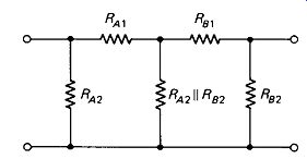
FIGURE 17-13 Cascading pads is sometimes advisable to avoid unreasonably low
resistor values, or to keep resistor values lower than stray capacitive reactance.
Notice that the output R2 of pad A is simply paralleled with the input R2 of pad B in cascading pi pads. In cascading T pads, the series equivalent to the two Rt values is used in a similar manner. Switched attenuators, having pads of 1 dB, 1 dB, 3 dB, 6 dB, 10 dB, 20 dB, and 20 dB are fairly common since they can be placed in or out of the cascade to give attenuations from 0 to 61 dB in 1-dB steps.
EXAMPLE 17-4 Find the resistance values required in Fig. 17-13 if the total attenuation required is 36 dB and Z„ = 600 ohm.
Solution
Each pad will give 18-dB attenuation:
From the pi-pad design formulas:
Continuously variable attenuators of the pi or T design would require ganging and odd-curve tracking of three pots. The bridged-T attenuator of Fig. 17-14 can be constructed using two conventional log-taper pots ganged together. The relevant equations are given with the figure.
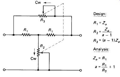
FIGURE 17-14 Bridged-T attenuator with design and analysis formulas.