This section presents a variety of circuits for generating and processing signals.
The circuits were chosen because of their widespread application, so you will be likely to encounter most of them in industrial electronic instruments and control systems. The commercial versions will often be augmented with noise filters, buffer amplifiers, range switches, and temperature-compensating circuitry, but an understanding of the basic circuits will enable you to see through all this to the basic function of the device.
19.1 CURRENT AND VOLTAGE CONVERSIONS
Current-to-Voltage Conversion can be achieved with the circuit of Fig. 19-1(a). The input terminal operates at virtual ground. The circuit is easy to understand if it is remembered that the op-amp input current is virtually zero. 7in must therefore be virtually equal to IR1, and Va = IR1 R1. The circuit is useful for currents from I_O (max) to approximately 20I_iN (bias) of the op amp, which covers ± 5 mA to ± 150 nA for the 308 op amp. FET-input op amps can extend the current down to the pico-ampere range.
Voltage-to-Current Conversion is accomplished by the circuit of Fig. 19-1(b).
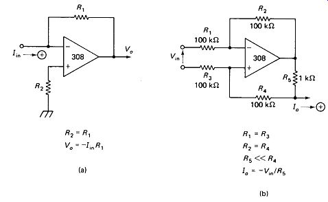
FIGURE 19-1 Current-to-voltage converter (a) and voltage-to-current converter
(b) with applicable formulas.
Picturing the circuit with the bottom of Rs grounded, it is easily recognizable as the differential-op-amp circuit with Va appearing across Rs, so that IR5 = Vo / RS. If R4 is much greater than R5, then I0 is nearly equal to IR5. Of course, it is not necessary that the bottom of Rs be at ground. Either input terminal or some point referenced to them can serve as ground, as long as the common-mode input range is not exceeded. Very low currents can be obtained by raising R1 and R3 (or lowering R2 and R4) by a factor of 10 to lower the dif-amp gain. The linearity of the current source as VQ changes requires a good match of the R2/R1 and R4/R3 ratios, so a trim pot in one of these positions is advisable.
AC to DC-The Perfect Diode: The circuit of Fig. 19-2(a) provides two outputs equal to the positive and negative half-cycles of an ac input, without the diode drop encountered with a conventional rectifier. Amplification of the output by any factor Rj/Rin is also possible. Any value of load resistance can be connected from either output to ground, provided that the op-amp output current limit is not exceeded. Where millivolts of output are important an offset-cancellation circuit is recommended.
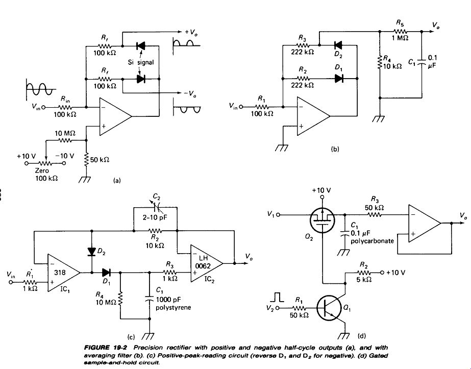
Fig. 19-2
Average Value of AC: Most ac voltmeters actually respond to the average value of a rectified ac wave, although this value is scaled to read in rms terms when the input is a sine wave. This is done because average is easier to obtain than true rms, but remains relatively more accurate in the face of non-sine waves and noise spikes than the other alternative, namely peak-reading. Figure 19-2(b) shows an addition to the perfect rectifier which produces a dc output proportional to the average value of the positive half-cycle input. The output impedance is quite high, so a noninverting amplifier is recommended as a buffer. A gain of 2 would fill in for the negative half-cycle, so a gain of 2(0.707/0.637), or 2.22, will give a dc output equal to the rms value of an input sine wave. The time constant of averaging filter /?5C, is 0.1 s, so the circuit will reach full response in about 0.5 s, which is considered an acceptable lag. Input frequencies below 50 Hz begin to show excessive ripple in Va, so a two-section filter may be required. R4 is necessary to preserve a near-zero source impedance for the filter when D2 turns off.
Peak Reading of AC: The circuit of Fig. 19-2(c) gives a dc output equal to the repetitive positive peak of the input wave. Feedback of V_o through R2 to the reference input of IC, ensures that v_o will equal v_IN, regardless of the drop across D1. D2 overrides this positive feedback during negative voltage inputs. Reversing D1 and D2 allows the circuit to read negative peaks. R4 discharges C, to allow the output to follow decreasing pulse heights. IC2 should be a low-bias-current FET input type and IC, should be a fast bipolar type for this application.
Peak-holding Circuit: The circuit of Fig. 19-2(c) will hold the maximum peak voltage of Va for several seconds if R4 is removed, leaving no discharge path for C1. Peak memory circuits are useful in detecting noise and other one-shot voltages. C1 should be sized to allow it to be charged by the shortest expected input spike using the familiar CV = It formula. For an op amp with a 5-mA output capability sensing 5-V pulses as short as 1 u-s:

(19-1)
Output droop rates as low as 20 mV/s are possible with the components specified.
C1 and D2 should have the lowest possible leakage in this application, and the voltage follower should contain an offset cancellation circuit. A pushbutton switch can be placed in the R4 position to reset the memory.
Sample and Hold: A common instrument problem is "What was the steam pressure when the pipe broke? " or some similar question requiring memory of a voltage at a particular critical instant of time. The circuit of Fig. 19-2(d) charges C, to the input voltage Vx when the sample command V2 goes positive. With V2 at ground, the collector is positive, holding / "channel FET Q2 off, isolating the charge stored on C1. R3 is for overload protection.
19.2 ADDING CIRCUITS
The most popular summing circuit is the add-and-invert op-amp circuit of Fig. 19-3(a). Operation is exactly the same as for the inverting amplifier of Section 16.2.
Any number of inputs can be used, and there is no interaction between them because the summing point (the - op-amp input) is at virtual ground.
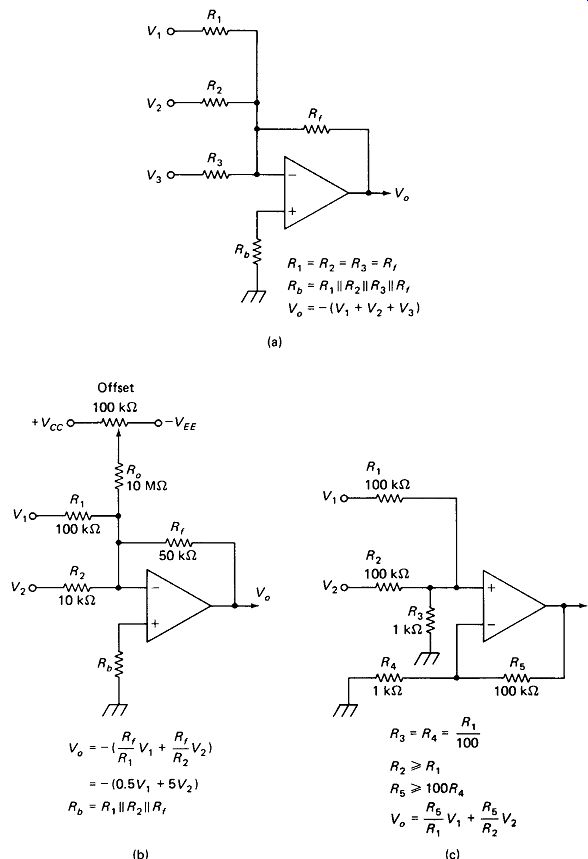
Fig. 19-3
Multiply and Add is effected by simply changing the value of the input resistors, as shown in Fig. 19-3(b). Each input is now multiplied by Rf/Rm before being summed. The final output is, of course, still inverted. Note that each input now presents a different input resistance. Unless Rs is hundreds of times smaller than each Ra, a voltage-following buffer [Fig. 16-2(b)] should be used on each input.
Where a few millivolts output offset would be a problem, or where Rf is in the megohm range, the offset-adjust pot and Ra are recommended. If inversion of the output signal is undesirable, a gain-of-one inverting amplifier can be placed after the summer to re-invert the output. If subtraction is to be performed, the subtracted input can be applied directly to the summer while the added input is first run through an inverter.
Figure 19-3(c) shows a circuit for noninverting addition in a single op amp. Any number of inputs can be used provided that the parallel combination of input resistances is much greater than R3. The gain factor for all inputs can be made greater or less than unity by making R5 smaller or larger, respectively. Different gain factors for each input can be realized by making R2 greater than R1 . The input resistance of this circuit is equal to R1 R2, etc., at each input.
19.3 MULTIPLYING AND SQUARING CIRCUITS
Multiplying a voltage by a constant factor is a simple job, requiring only a basic amplifier. Multiplying a voltage by another voltage, both of which are varying, is more of a challenge. Measuring the IV (power) product when an odd-shaped waveform appears across a load that is not a simple resistance presents one application for a multiplying circuit. SCRs and switching transistors often produce such waveforms.
Photocell Multiplier: Figure 19-4(a) shows a multiplier in which K, is used to control the gain of the amplifier fed by V2. When V, is +1 V, the IC, through emitter-follower Qx, applies enough negative voltage to lamp /, to make the PC, resistance 100 k ohm, thus keeping the op-amp input at virtual ground. The photocells are a matched pair, equally coupled to /,, so PC2 likewise has R - 100 k-ohm, making the gain of IC2 unity. Two volts at Vx will make RpQ = 50 k ohm, yielding an IC2 gain of two, and so on.
The accuracy of this system depends upon the matching of the photocells.
Prepackaged pairs matched to within 1% can be obtained. A more serious draw back in most applications is the response speed, which is limited to a few tens of hertz by the photoresistive cells. Notice that this is a two-quadrant inverting multiplier. V2 may be positive or negative, but Vx must be positive..
Dif-Amp Multiplier: Figure 19-4(b) shows a two-quadrant multiplier with a response speed that can extend into the megahertz range with proper design and selection of the op amps. As in the first circuit, K, controls the gain of V1V2, but this time the Variable resistance is the emitter-junction resistance of the transistors in the dif-amp Q,-Q2, which is approximately 0.03/I_E.
V1, which must be positive, supplies a current between 0 and 2 mA to the two emitters of the dif amp, varying their total resistance from infinity to 2(0.03/0.001) = 60 ohm. The gain of the dif amp thus varies from zero to 600/60 = 10.
V2 is divided down by a factor of 100 to provide a low-impedance low voltage to drive the base of Qx. Higher base voltages would result in V2 controlling the gain of the dif amp. IC2 provides a gain of 10 and restores the output from floating differential to single-ended ground referenced.
Pulse-rate Divider: An approach to analog division that is capable of very high accuracy, but is limited in frequency response, is shown in Fig. 19-4(c). IC, free-runs with a period of about 500 u-s with VA = 5 V. This is calculated from R1 current and C, charging time:
Increasing VA lengthens the period proportionally, since the Control voltage equals the Threshold voltage to which C1 must charge to end the cycle.
IC2 is triggered by IC1 at f= 1 /t1, but the duration of its output pulses is controlled by VB. For VB = 5 V, t2 is about 50 u-s.
The train of pulses at pin 3 of IC2 is thus approximately 10 V high, with a duration of 50 u-s, repeating every 500 u-s-an average value of 1 V. Increasing VB lengthens the pulse duration, thus increasing the average value proportionally. Increasing VA decreases the repetition rate, decreasing the average value proportionally.
Filter R3C3-R4C4 converts the pulse train to dc of its average value. The filter’s cutoff is 32 Hz, so repetition rates above 1 kHz are attenuated by at least 60 dB. This is the minimum frequency, corresponding to VA = 10 V.
The 100-V supply and 100-k Ohm resistors are a simple but crude method of obtaining a fairly constant 1-mA charging current for C1 and C2. Substitution of the PNP-transistor current source shown in Fig. 9-6(a) will greatly improve accuracy. The voltage-Variable IC current source of Fig. 19-1(b) may be used in place of Rx to provide a third multiplying input.
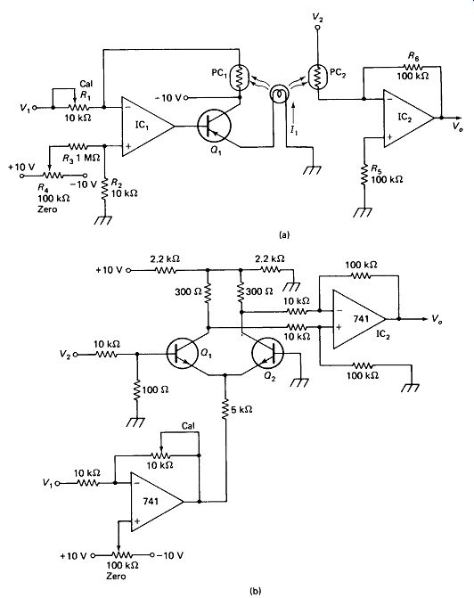
Fig. 19-4
FIGURE 19-4 (c) Analog division: VA controls rate and VB controls duration of pulses out of IC2- Averaging fitter smooths pulses to varying dc.
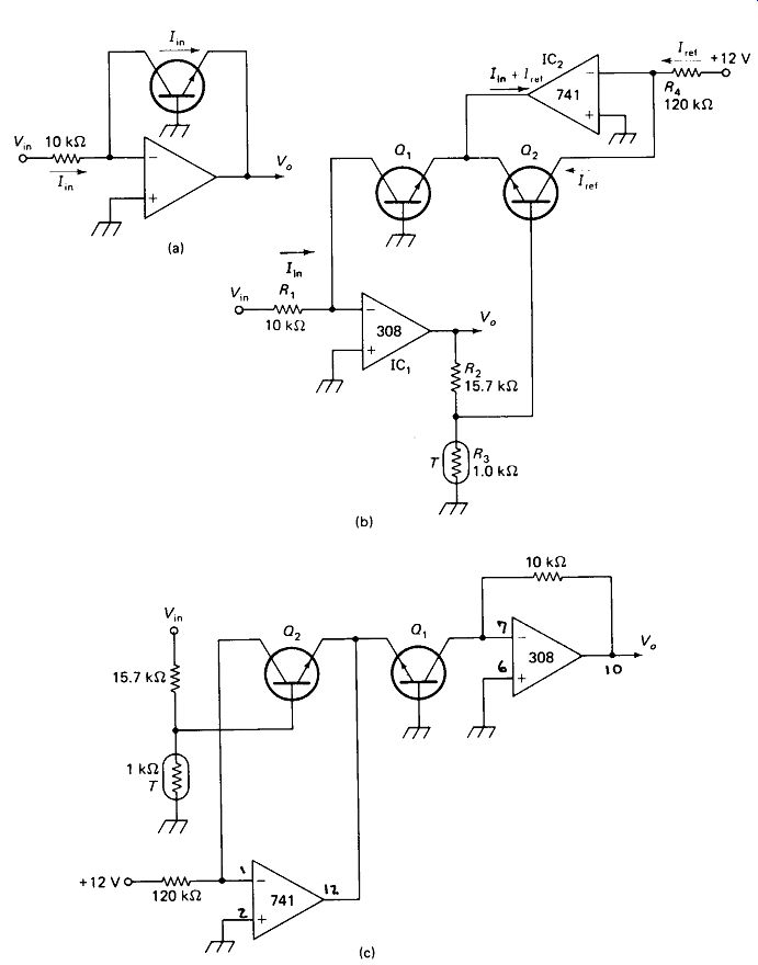
Fig. 19-5
Squaring a Voltage can be accomplished by connecting V1 to V2 in any of the multiplying circuits described above. In addition, there are nonlinear input elements especially designed to produce Va = when used in place of R in a simple inverting op-amp circuit. Squaring is useful in obtaining true rms values from a waveform of arbitrary shape. It should be noted that this mathematical squaring is not the same sis signal squaring (i.e., producing a square wave from an analog input signal).
19.4 LOG AND ANTILOG GENERATORS
The voltage across a silicon transistor's base-emitter junction is proportional to the logarithm of its junction current to within 1% from 0.05 /xA to 500 /x A, and this property can be exploited to produce amplifiers with outputs equal to the log (or antilog) of the input. This is useful because adding the logs of two voltages and taking the antilog produces the product of the two voltages. Similarly, multiplying a log by two produces the square, subtracting logs produces the quotient, and dividing logs produces roots of input voltages.
Figure 19-5(a) shows the basis of the log generator. Note that the output voltage is be which increases as the log of input current, since IE = Im- There are several problems with this basic circuit:
. There is an output offset voltage Vbe*
. The output voltage is proportional to absolute temperature as well as to log V,a.
. The output is inconveniently small, covering less than 0.1 V for a factor-of-10 change in Fin
.The circuit of Fig. 19-5(b) corrects each of these deficiencies. Q2 is fed by current-source IC2 with a current equal to the Qx current at Vin = 1 V.
Thus Va = 0
... when Vin = 1 V, corresponding to log 1 = 0. Voltage divider R2 - R3 increases V0 to 16.7(KB£, - VBE2), and thermistor R3 increases amplifier gain at higher temperatures, compensating for lower Vbe-
The output of this circuit is - 1 V for Vm = + 10 V, 0 V for = + 1 V, + 1 V for Vin = +0.1 V, and so on. Only positive inputs can be handled, and the output is, of course, inverted.
Figure 19-5(c) shows an antilog generator which places the transistor base emitter junction in the input rather than the feedback loop of the op amp. The input may be positive or negative, but the output will always be positive: + 10 V out for - 1 V in, + 1 V out for 0 V in, +0.1 V out for + 1 V in, and so on.
True rms Voltmeter: A system for performing the root-of-the-mean-of-the-square operation is given in block-diagram form in Fig. 19-6. The blocks are all circuits that have been described in this section. The design is simplified somewhat by the fact that the thermistors can be eliminated when an antilog generator follows a log generator.
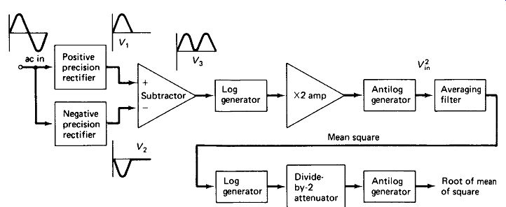
FIGURE 19-6 Block diagram of a true rms voltmeter based on square and square
root by multiplying and dividing logs.
19.5 INTEGRATION AND DIFFERENTIATION
Integration is a mathematical operation of calculus which is widely used in electronic circuits. Without going into the mathematical details, integration is simply a process of accumulation. Thus a 1-V input, integrated, would produce 0 V out initially, 1 V after 1 s, 2 V after 2 s, and so on, as shown in Fig. 19-7(a). A 2-V input produces a faster accumulation, and a negative input produces a negative accumulation, as shown in Fig. 19-7(b) and (c), respectively. It follows that the integral of a ramp (o - /) is an exponential rise (o = t2), the integral of a square wave is a triangle, and the integral of a string of pulses is a staircase, as illustrated in the next three parts of Fig. 19-7. A less obvious, but equally true, relationship is that the integral of a sine wave is a negative cosine (90° lagging) wave.
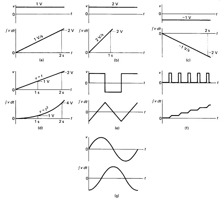
FIGURE 19-7 Integration is a process of accumulation: seven examples.
A little reflection will reveal that the output of an integrator depends upon the history of the input-what has been accumulated in the past. Therefore, every integration includes a constant-a dc voltage which may have been accumulated from previous input. In practical integrators the accumulated dc voltage can easily exceed the saturation limits of the circuit. Therefore, it is generally necessary to provide a reset function to return the integrator output to zero.
A Practical Integrator is shown in Fig. 19-8(a). For the example values given, the input resistor’s current is 1 pA. Since the op-amp input current is virtually zero, the capacitor must carry virtually this same 1 uA current. The op-amp output will ...
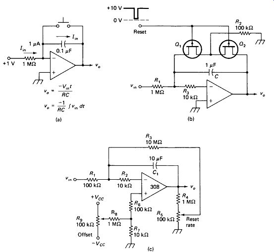
FIGURE 19-8 (a) Elementary integrator with switch reset, (b) Electronic reset
with FETs. (c) Low-drift self-resetting integrator.
... produce any voltage necessary to make Ic = 1 uA.
The output required is found from the CV = It formula:
= 10 V/s
The capacitor voltage (and hence the output voltage, since one end of the capacitor is at virtual ground) must rise at a rate of 10 V/s to keep a current of 1 u A flowing.
This corresponds to Fig. 19-7(a): the integral of a constant dc input is a ramp output. Actually, the ramp is negative for a positive dc input because the inverting input of the op amp is used.
After about 1 s the output of this integrator reaches saturation and the capacitor must be discharged through the pushbutton switch to reset the integrator to zero.
Electronic Reset can be achieved by replacing the pushbutton switch with an FET.
In some cases the leakage of the FET in the OFF state may be an appreciable fraction of the capacitor current, upsetting the circuit operation.
Figure 19-8(b) shows a scheme for greatly reducing the effects of FET leakage.
With Q1 and Q2 off, R2 presents a relatively low impedance to ground for the Q2 leakage current, while Q1 presents a relatively high impedance back to the -input of the op amp.
The 10-k R resistor R3 is recommended wherever the feedback capacitor exceeds 0.
1 pF to protect the IC in the event power is shut off while C is charged.
A Zero-Drift Integrator is shown in Fig. 19-8(c). No reset circuit is shown because the integrator will eventually return itself to zero if the input is held at zero.
The other integrators shown will eventually drift into saturation with zero input and no reset operation because of op-amp bias and offset currents.
Offset-cancellation circuits can reduce this drift by two or three orders of magnitude, but they cannot eliminate it entirely.
The circuit of Fig. 19-8(c) minimizes drift with bias compensation R6 and offset cancellation Ry, Rg, and R9. It also uses a low-bias-current op amp and the highest practical value of feedback capacitor to ensure that capacitor current is many orders of magnitude greater than input offset and leakage currents. R}, R4, and Rs are then used to introduce a very slight amount of negative feedback to restore the output to zero. This introduces a slight distortion into the integrating function, so that a linear ramp would actually be curved slightly toward zero.
At maximum reset rate with Va= 10 V the feedback current through R3 is 100 nA. This is enough to completely overcome a 10-mV input or cause a 10% distortion on a 100-mV input at R1. If a lower reset-rate setting can be used, or if Va is less than 10 V, the distortion will be correspondingly less. The reset action follows a conventional RC discharge curve with a time constant of about 15 min at maximum reset rate.
In operation, the input is grounded and the R5 wiper is set to the ground end.
R9 is then adjusted for a VQ that holds as nearly constant as possible on a sensitive scope or meter. R5 is then brought up slowly until the output holds as nearly as required to zero. The term slowly here should be taken to mean a check every minute or so. It goes without saying that C, must have the lowest possible leakage for this application.
Differentiation is the inverse operation of integration. Conceptually, the derivative, as the result of differentiation is called, can be described as the rate of change of the input variable. Looking at the several graphs of Fig. 19-7 it will be seen that in each case the upper curve represents the rate of change (in V/s) of the lower curve.
Therefore, if we integrate a function and then differentiate it, we get the original function back again.
Practical differentiators must make some compromise with true mathematical differentiation because reasonably fast-rise pulses can demand unreasonably high output voltages. Furthermore, noise pulses tend to be fast-rise and are greatly overemphasized in true differentiation.
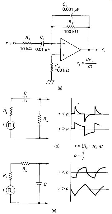
FIGURE 19-9 (a) Practical op-amp differentiator, (b) Simple RC differentiator
with waveforms showing maximum and too-long time constants, (c) Simple RC
integrator with waveforms showing too-short and minimum time constants.
In the differentiator of Fig. 19-9(a), R1 limits the input current to 0.1 mA/V regardless of the rate of rise of input voltage. C2 shunts R2, lowering the gain at high frequencies. C, and R2 are the basic differentiator components. Noise response can be reduced by increasing Rx and C2. Signal response can be increased by increasing C, and R2.
RC Differentiators and Integrators: This seems a good place to note that simple RC circuits are often used to approximate differentiators and integrators, as shown in Fig. 19-9(b) and (c). The RC differentiator is nearly as good as the op amp version because of the limits that must be placed on the op amp differentiator. The RC integrator resets to zero through Rt and Rs as fast as it accumulates, and therefore produces a poor approximation to true integration. For these reasons, RC networks are most often used for differentiating and op amps are most often used for integrating.
19.6 INTEGRATOR APPLICATIONS
Rate Limiter: Figure 19-10(a) shows a circuit in which the output will follow the input voltage, subject to the limitation that the output rate of change cannot exceed 2 V/s, or whatever other limit is selected by integrator components R3 and C,. The inversion of IC2 gives a negative feedback signal to R4 which is balanced against the positive signal across R1 . IC, saturates if the input rate of change exceeds the integrator’s limit. Gain can be added by increasing R4 or lowering R1 . Rate limiters are useful in industrial process controllers, where rapid changes in position, velocity, temperature, and so on, would be damaging to the process.
Staircase Generator: A square wave, when differentiated, will produce a string of positive and negative pulses. If the pulses are rectified and integrated, a staircase output will result. Figure 19-10(b) shows the implementation of this concept. A precision rectifier IC, is used to avoid the temperature sensitivity of a simple diode.
Integrator IC2 is reset by hysteresis switch IC3.
19.7 ANALOG AND DIGITAL CONVERSION
Voltage Comparator: The circuit of Fig. 19-11(a) will output a positive saturation level (about +9 V for ± 10-V supplies) if V1 is greater than V2, and a negative saturation level if V2 is greater than Vv
Schmitt Trigger: The circuit of Fig. 19-11(b), also called a hysteresis switch, is similar to the voltage comparator except that it tends to remain in its present state until an overvoltage at one input forces it to snap to the other state. The circuit is most often used with V2 at ground, but in any case V2 should not be allowed to become a large fraction of the supply voltage. The hysteresis or dead zone is calculated as ...
FIGURE 19-10 (a) Rate limiter: v„ follows v/n except that the v„ rate or change
cannot exceed the limit set by R3L and CL1. (b) Staircase generator composed
of differentiator C,R f, perfect rectifier IC,, integrator IC,, and reset switch
IC3.
FIGURE 19-11 (a) Simple voltage comparator, (b) Positive feedback forma a
hysteresis "snap-action" switch, (c) Voltage divider R4RS gives smaller
dead zone with reasonable values of R3.
For the values given in Fig. 19-11(b) this means that the output will remain in its current state as long as K, does not differ by more than ±0.9 V from V2.
Very small dead zones are often desirable, but often result in unrealistic values of R3. Figure 19-11(c) shows a method for reducing dead zone by a factor of (R4 + R5)/R5.
Schmitt triggers find a wide variety of applications. They may be used as:
. Level detectors, to activate a relay or light when a preset voltage is exceeded, and leave it activated until the level drops significantly below the set level
. Snap actuators, to prevent a relay from mushing in uncertainly on levels near the actuate point
. Bounce eliminators in conjunction with an RC filter to prevent a separate actuation for each bounce of a switch contact
. Square-wave generators, to produce two-state digital outputs from sine or similar analog inputs
Digital-to-Analog Conversion can be accomplished with the simple summing circuit of Fig. 19-12. The values shown give an output of 1 V/count, although 0.1 V/count could be obtained by making Rf= 8.0 k-Ohm. The I_s through 8s lines are the outputs of a binary or BCD counter, such as the 7490. The 4016 quad analog switch is used, gated by the binary outputs, because the counter outputs themselves have levels which may vary by a few tenths of a volt among outputs and with temperature. The CD4016 actually contains a pair of insulated-gate FETs for each gate. The input-to-output assumes a very low resistance (around 100 ohm) when the control line is high, and a very high resistance (many MB) when the control line is low.
More inputs can be added for 16-s, 32-s, and so on, but as the summing resistor values become lower, their tolerance becomes more and more critical. A 3% error in the 32-s resistor will completely swamp out the contribution of the 1-s resistor. Integrated D/A converters are available with 8-bit (256 count) resolution.
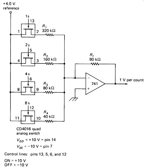
FIGURE 19-12 Digital-to-analog converter using precision resistors and the
CD 4016 CMOS IC.
Analog-to-Digital Conversion is a bit more of a challenge than D/A conversion.
Many methods have been developed for A/D conversion, but we will describe only two: a simple one and the one most widely used in DVM circuits.
The Continuous-Search A/D Converter, shown in Fig. 19-13(a) incorporates the D/A converter of Fig. 19-12. The analog output is compared to the input voltage, and the binary counter is directed to count up or down, as required to equalize the comparison. Of course, the counter always counts up or down at least one count each clock pulse, and this instability can be quite annoying in a visual display. A timing gate on the clock (Is hold, 0.1 s count) will alleviate this problem. This converter can be made quite fast, but its accuracy is limited to about \% by the D/A converter. A slower version eliminates the up/down counter, resetting to zero and counting all the way up each display cycle.
The Dual-Slope A/D Converter of Fig. 19-13(b) is the basis of most commercial digital voltmeters. It can be made highly accurate, since its basic function is to measure the ratio between the input voltage and an internal reference voltage. The tolerance and stability of all the resistors, capacitors, and semiconductors in the circuit do not affect the final accuracy of the conversion-only the accuracy of the reference supply is important.
At the start of the conversion cycle the flip-flop is reset, so Q2 is turned on by the low level at its gate, while Qx is turned off by +5 V at its gate. The integrator thus generates a negative ramp at a rate of 5 V/s for a + 0.5-V input. As soon as this ramp crosses zero, the comparator output goes positive, enabling the AND gate and starting the counter. Let us assume that the counter is a three-stage BCD type counting to 999. Also, let the clock rate be 5 kHz. The integrator will thus reach - 1 V output in the 0.2 s it takes for the counter to reach maximum count.
The highest-order bit of the counter feeds an overflow flip-flop which is set as the counter advances from 999 to 000. This sets the control flip-flop, disconnecting Vin and connecting V-ref to the integrator via Qt.
Note here that the time required for the count from 000 through 999 and back to 000 depends upon the clock frequency and is relatively constant. However, the slope of the integrator output, and hence the voltage reached as the counter rolls back to 000, depends directly upon Vin.
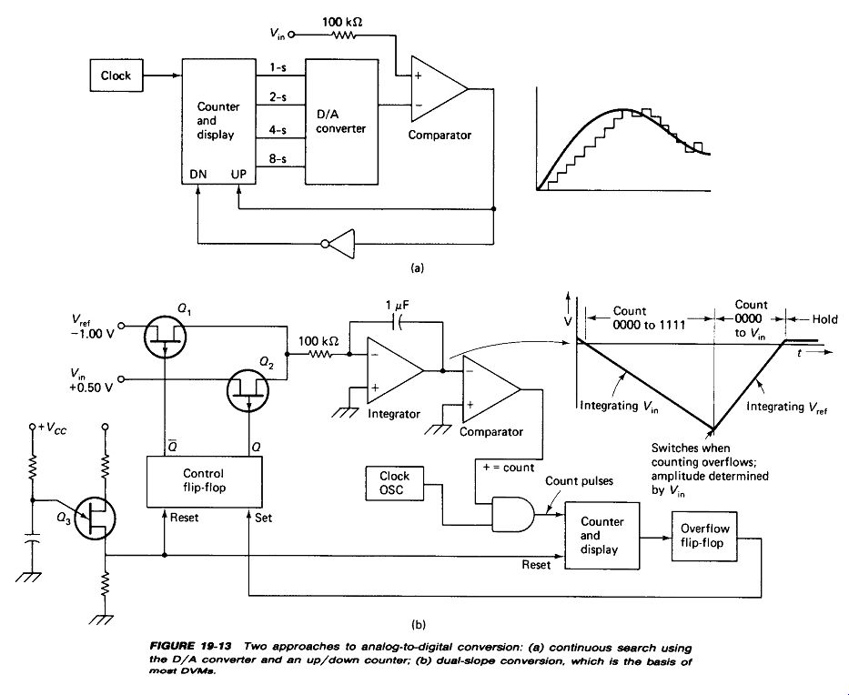
Fig. 19-13
Now the counter begins counting again up from zero, but this time the integrator output is rising at a rate of 10 V/s, as determined by K«- The run back to zero from -1 V will take 0.1 s, and at 5 kHz the counter will read 500 at the zero crossing. The counter will stop at this point because a positive integrator output will set the comparator output negative, disabling the AND gate to the counter. This value will be displayed until the UJT Q3 fires (after a second or so), resetting the control flip-flop and starting a new cycle.
If the integrator resistor or capacitor should be a little low in value, the negative ramp would be a little steeper, and the peak voltage would be a little higher, but this would be of no consequence because the positive ramp would be a little steeper by the same percentage. Likewise, if the oscillator should run a little slow, the time to reach the negative peak would be a little longer, but the time to return to zero would be longer by the same percentage, and the final count would be unaffected.
19.8 VOLTAGE AND FREQUENCY CONVERSIONS
Frequency-to-Voltage Conversion is a simple matter of generating standard length pulses at a rate equal to the input frequency and averaging the value of the pulses with an RC filter. Figure 19-14 shows one approach using a UJT and another using an IC one-shot. F/ V converters form the basis for tachometers and frequency meters.
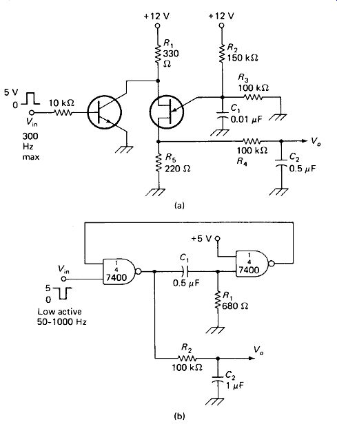
FIGURE 19-14 Frequency-to-voltage conversion: standard pulse widths are generated
at the input trigger rate and averaged by an RC filter.
Voltage-to-Frequency Conversion using the control input of a 555 oscillator has already been encountered in Fig. 19-4(c). Better linearity can be achieved with an integrator driving a 555 level detector, as shown in Fig. 19-15. For the values given, IC, will integrate at +1 V/ms for a - 1-V input, reaching the 555 threshold in 6.7 ms. The output of ICj will then go low, turning Qx on and discharging C,.
Discharge will continue until the trigger input of the 555 goes below 3.33 V. R4 is adjusted so that this will happen as nearly as possible to zero output from the integrator. The discharge time is a negligible fraction of the 6.7-ms charge time.
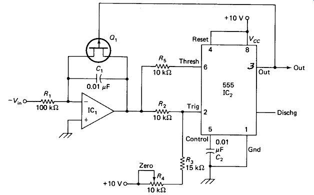
FIGURE 19-15 Voltage-to-frequency conversion: integrator IC, reaches threshold
2/3 Vcc in a time determined by Vin, whereupon Q1 resets the Integrator.
Once pin 2 of IC2 goes below 3.33 V, the output goes high and Q1 turns off, initiating another integration period. The integration time to the 6.7-V threshold is directly proportional to V_in.
In this case, with V_in = - 1 V, the output frequency is 1 /6.7 ms, or 150 Hz.
19.9 SIGNAL GENERATION
Oscillators are of three basic types:
--- Feedback oscillators feed the output signal in phase back to the input in a regenerative process. The basic requirements here are a total phase shift around the loop of exactly 0° or 360°, and a total loop gain (Av X feedback ratio) equal to unity. Loop gains greater than unity produce progressively more severe distortions of the sine-wave output. Frequency is determined by the phase-shifting components, which may include the input and output resistances of the active device in the amplifier. These parameters vary with bias point, making supply voltage a determiner of frequency to a small extent. The phase shift of a tuned circuit varies abruptly from inductive to capacitive around resonance, so transistor parameters cause less frequency shift in a tuned-circuit oscillator than in a phase-shift type. Higher-Q tuned circuits produce better stability. The quartz crystal, with Q's above 20,000, stands as the paragon of stability. FET inputs with emitter-follower buffers before the feedback loop will keep the input resistance near infinity and the output resistance near zero, reducing the effects of the active devices.
-- Relaxation oscillators charge a capacitor until some trigger device reaches its threshold, whereupon the capacitor is discharged, and the cycle repeats. Common trigger devices include neon lamps, UJTs, transistor switches, IC logic gates, and op amps. Relaxation oscillators generally produce ramp and square-wave outputs. Frequency is dependent upon the capacitor value, the charging rate, and the trigger threshold. These last two factors are often dependent upon power-supply voltage and/or temperature, making a high degree of stability difficult to obtain.
-- Negative-resistance oscillators incorporate an LC tuned circuit and a suitably biased negative-resistance device to cancel the positive resistance representing coil losses and energy coupled to the load. The result is a zero-resistance LC circuit which maintains oscillations without damping over the negative-resistance range of the device. Bipolar transistors, UJTs, diacs, and other devices have negative-resistance regions, but maintaining a stable bias point within them is difficult. The tunnel diode is easily biased in its negative-resistance region, but the dynamic range (and hence oscillator output) is limited to a few tenths of a volt.
A Wien Bridge Oscillator, which retains the frequency stability and sine-wave purity of an LC-tuned oscillator while dispensing with the inductor, is shown in Fig. 19-16. At the frequency where X_C1 - Rx and X_C2 = R2, the Wien bridge forms a 21:1 voltage divider with both series and parallel arms having a 45° current-to voltage phase angle. The feedback is therefore positive, and a gain of 21 will make the circuit oscillate. At other frequencies the series and parallel arms will have differing phase angles, producing a feedback that is not exactly in phase.
R3 and the drain resistance of Qx must have a ratio of 20:1 to produce the required gain. This is accomplished by sensing the output waveform and using it to change the gate bias, and hence the dynamic drain resistance of the FET. Output peaks above -5.3 V charge C3, applying a negative dc to the gate of the FET, raising its drain resistance and lowering the gain of the amplifier. This tends to lower the output peaks. In fact, the output peaks will be greater than ± 5.3 V by an amount equal to the Vgs required to produce a drain resistance of 500 ohm.
FIGURE 19-16 Wien-bridge oscillator. R3 and Q, determine the gain of IC1. Q1
is biased off by excessive output, lowering gain to prevent distortion.
A Phase-Shift Oscillator with two sine-wave outputs 90° apart (quadrature outputs, they are called) is shown in Fig. 19-17. IC, is an integrator, which assures that the output phase lag is exactly 90°.
This is so because the integral of the sine is the negative cosine, which is a 90° lag. The integrator is followed by two RC phase-shift networks, each providing 45° lag at the frequency where Xc = R. The total 180° lag, combined with the inversion of the integrator, produces an in-phase feedback.
The wave is limited by D1 and D2 after the first phase-shifting section to make the feedback adjustment R5 a little less critical. There are what amounts to two low-pass-filter sections between these limiters and the IC output, which will keep the resulting harmonic distortion at a low level. Without D1 and D2 the IC output would go to its saturation limits, producing heaviest distortion at the output.
A Relaxation Oscillator which amounts to a simple function generator is shown in Fig. 19-18(a). It consists of a Schmitt-trigger level detector (Fig. 19-11) driving an integrator (Fig. 19-8). The integrator output is driven positive by the negative saturation level output of IC,, applied through voltage divider R3 R4 and current limiter R5. When the positive ramp output on R1 overcomes the negative saturation level on R2, the Schmitt-trigger output switches to positive saturation, ending the positive ramp and starting a negative ramp from the integrator.
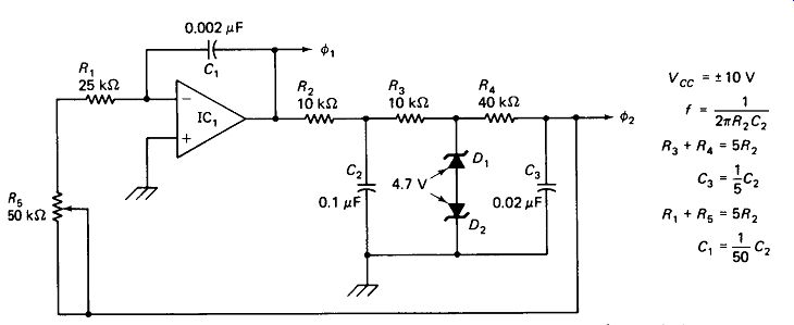
FIGURE 19-17 A quadrature oscillator has two outputs, 90° out of phase.
Integrator IC1 guarantees exactly 90 degree shift since the integral of the cosine is the sine. R5 is adjusted for purest sine wave with D1 and D2 just conducting.
R3 varies the output frequency over a 20:1 range, and C, can be switched by decades from 10 uF to 0.001 uF to produce an output range from 0.5 Hz to 100 kHz.
The resistor and diode network from the triangle output places successively heavier loads on R1 as the triangle reaches its peaks, thus loading it down to an approximate sine-wave shape. With only two break points on each half-cycle the segmentation of the " sine" wave is rather obvious (about 2% harmonic distortion), but commercial units with five or more break points bring the distortion down to 0.2% and less.
A Voltage-Controlled Function Generator is shown in Fig. 19-18(b). Analysis shows that current to the inverting input with Qx on is equal in magnitude but opposite in sign to the current with Qx off. The following calculations are done referenced to the - 10-V supply as a temporary "zero."
Circuit ground thus becomes + 10 V in the calculations. This simplifies the arithmetic, since the voltage dividers are all referenced to - 10 V:

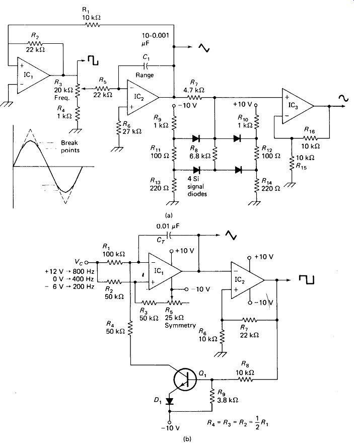
FIGURE 19-18 (a) Variable-function generator with sine, square, and triangle
wave outputs, (b) Voltage-controlled function generator. Vc determines output
frequency.
Returning the reference to circuit ground, this means that Vc =» - 10 V produces a zero integrator current and zero frequency (ideally), - 9 V produces /, - 8 V produces 2/, -5 V produces 5/, 0 V produces 10/, and +5 V produces 15/.
19.10 THE PHASE-LOCKED LOOP
The phase-locked loop has appeared in sophisticated communications systems for quite a few years, but its availability as an inexpensive integrated circuit has led to its application in entertainment receivers and a widening variety of non-communications equipment.
Integrated phase-locked loops (PLLs) have two distinctly different applications:
. They can be used to produce an output voltage level that varies with the frequency of the input signal. In some devices the K-versus-/ curve is extremely linear over a limited range, although it is not zero-based (zero frequency does not produce zero voltage). In this mode PLLs are commonly used as FM detectors and FSK (frequency-shift keying) Teletype demodulators.
. They can be used to produce an output frequency that is locked to the frequency of an input signal-even though the input may be modulated, badly distorted, covered with noise, or even interrupted. The output wave, of course, will be perfectly clean, and will follow the input frequency over a limited range if it should vary. In this mode, PLLs are used as frequency synthesizers, automatic frequency-controlled oscillators, and signal re-constructors.
A phase-locked loop contains a voltage-controlled oscillator, a phase detector, and a low-pass filter. Of the three, only the phase detector requires explanation at this point.
A Phase Detector is a circuit designed to produce an output proportional to the phase difference between two input signals. Ideally, if f1 = f0 the output would be dc-positive if f leads fa, negative if f1 lags f0.
The magnitude of the dc would be directly proportional to the phase difference. If / were slightly different from fa, the phase detector output would be a low-frequency ac (frequency -/„) going positive and negative as f1 and f0 fell in and out of phase.
Real phase detectors are not quite so clean. They are actually a form of multiplier (o, t>0 ) or mixer, similar to the mixer in a superheterodyne receiver. The outputs actually obtained are the difference (f -fa), the sum (f +fB), and, if the mixer is not perfectly balanced, the inputs / and fa.
To make matters worse, f„ is usually a square wave, and f is processed through an amplifier that generally saturates, making/ a square wave. This means that 3rd, 5th, 7th, and higher odd harmonics and all their possible sums and differences are also present in the output. The only salvation in all this confusion comes from the fact that, if ft differs from/,by no more than 10%, none of the harmonics below the 19th and 21st will be able to mix with anything else to produce a frequency as low as ft - fa.
For a 5% difference the lowest harmonics that can cause trouble are the 39th and 41st, and for a 1% difference it becomes the 199th and 201st. A low-pass filter can thus be used to remove the ft+f0 component, and all the components due to significantly strong harmonics.
An Integrated Phase-Locked Loop, the type 565, is shown in Fig. 19-19. Comments on the characteristics of each part of the device may be appropriate before explaining some of its applications.
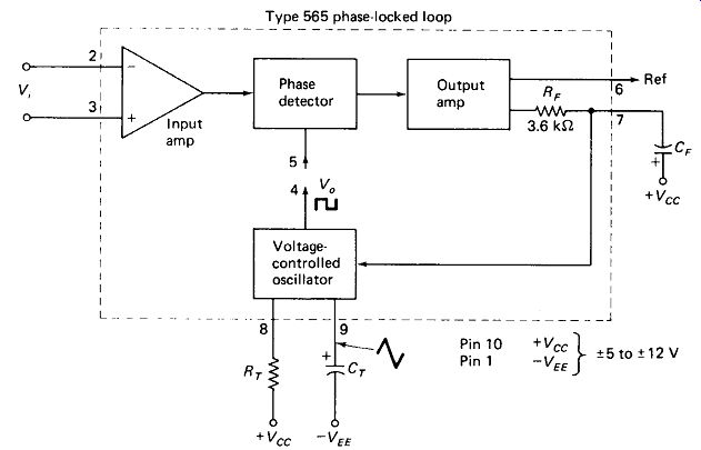
FIGURE 19-19 The type 565 phase-locked loop: internal functions and pin designations.
The Input Signal may be differential, with common-mode limits of +1 and - 4 V, although pin 3 is usually grounded. Input impedance is typically 10 k-ohm between inputs, but much higher to ground. Minimum input is about 25 mV p-p,
with saturation a certainty by 200 mV p-p. Bias and offset currents are in the ju A range and can easily shift one input more than 100 mV from the other, saturating the amplifier and locking out Vt. High source impedances should therefore be avoided.
If ac coupling is used, both inputs should be tied to ground through 4.7 k-ohm.
The Phase Detector produces a voltage at pin 7 which is referenced to + Vcc and ranges from about 1 to 3 V below this level for Vi to VB phase differences from 30° to 150°, respectively. It is driven by square-wave Va (pin 4 connected to pin 5) which swings from about -0.2 to +5.0 V, for a ±6-V supply.
The Low-Pass Filter is most often a single-section RC type. The resistance is an integrated 3.6 k ohm since this allows temperature tracking with the VCO components.
The capacitor is external and is selected to filter out + fa without attenuating The capacitor is referenced to the + *cc supply because this is the reference for the phase detector and the VCO. Grounding the capacitor would introduce power-supply noise and ripple into the VCO input. More complex filtering is possible by feeding from pin 7 to the filter to a current source to pin 8. Manufacturer's application notes describe this technique.
The Voltage-Controlled Oscillator operates up to 0.5 MHz. (The type 560 PLL operates up to 30 MHz.) Oscillation frequency is given approximately by:
f0=0.3/RtCt (19-3)
This frequency will be multiplied by approximately 0.5 with the VCO input (pin 7) 1 V below + Vcc, and by about 1.5 with pin 7 at 3 V below + cc. This is a total voltage-control range of 3 : 1. It is recommended that the timing resistor be restricted to the range between 2 and 20 k-Ohm. A 2.5-V-p-p triangle wave is available at pin 9 (Vcc = ± 6 V), although loading this output will slow and eventually stall the VCO. The timing capacitor can be referenced to ground, or if an electrolytic is required, to cc to avoid reversing polarity voltages on it.
Single-Supply Operation of the 565 PLL is possible if the inputs are biased about 1 V lower than 2 K:c through resistances of 10 k-Ohm or less. The square- and triangle-wave outputs will not cross, or even come near ground level in this case, but that is often of no consequence.
An FM Detector using a PLL is shown in basic form in Fig. 19-20(a). Capacitor CT is determined from equation 19-3 to make the VCO oscillate at a center frequency equal to the FM input with RT chosen as 10 k ohm:
The filter capacitor is chosen to attenuate the f, + fB output of the phase detector (2 kHz) by a factor of 100. This places the fc breakpoint of the Bode plot at 20 Hz, which means that the output of the detector will be severely attenuated if the 1-kHz carrier is modulated at a rate higher than 20 Hz.
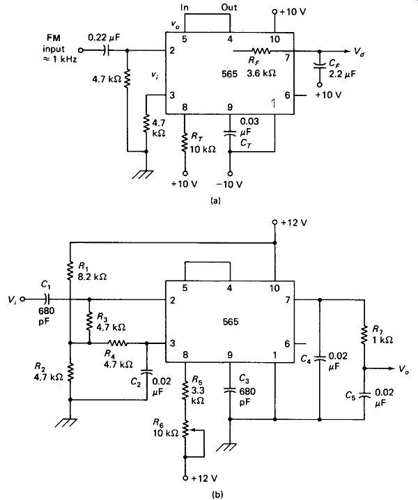
FIGURE 19-20 (a) FM detector suitable for testing the 565 PLL. (b) FM detector
for SCA music subcarrier detection.
In operation, the VCO will follow the frequency of the FM input. This is so because as / increases, putting the phase of V, ahead of V0, the phase detector produces a more-negative output, which increases f0 until the two frequencies match. Similarly, a decrease in will raise Vd, lowering the VCO frequency/, to match fr Vd is thus a demodulated output. Note that the output impedance is 3.
6 k-Ohm.
Figure 19-20 is a good circuit to build to become familiar with basic PLL characteristics. It can be observed that the waveshape and amplitude of I, (down to 10 mV or so) have no effect on Vd. Two signal generators can be placed in series at V, to demonstrate that noise and interfering signals are ignored as long as they are not too strong and too near fa. A graph of / versus Vd can be constructed to discern the linearity of the FM-detection process.
Lock Range is the span of frequencies above and below /„ for which the VCO will follow For the 565 this is typically ± 50% around f0.
A more precise expression is:

(19-4)
... where f_lock is the span between upper and lower lock frequencies, fa is the VCO center frequency, and Vcc is the total supply voltage between pins 1 and 10.
Capture Range is the span between the upper and lower frequencies at which the VCO will snap into lock if is brought toward fa from far outside the lock range.
Capture range is narrower than lock range, and becomes narrower yet as the time constant of the filter RFCF is increased:
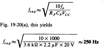
(19-5)
For the values in Fig. 19-20(a), this yields....
This means that VCO center frequency fa must be within ±125 Hz of or the VCO will be unable to lock to f_in.
Sometimes it is desirable to decrease the lock and capture ranges of a PLL.
Tone decoders (touch-tone dialing) must have a narrow lock range. Where several signals are present at the input, a wide capture range makes the PLL apt to lock in on the wrong one. A resistance of 5 k-Ohm between pins 6 and 7 of the 565 will reduce the lock range by approximately one-half. Shorting pins 6 and 7 will cut the range to about one-fourth.
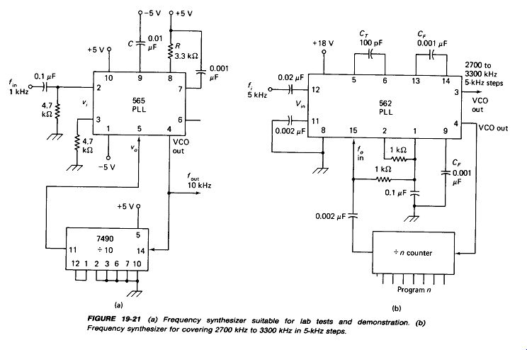
Figure 19-21
Figure 19-20(b) shows a practical FM detector for the 67-kHz SCA (subsidiary communications authorization) subcarrier that is broadcast by some FM stations.
This subcarrier is available at the detector of a regular FM receiver, but is generally attenuated through the audio-amplifier stages because of its high frequency. This service is sold on a subscription basis and carries background music suitable for offices, shopping areas, waiting rooms, restaurants, and so on. Note that it is illegal to use this service on a public or for-profit basis without paying the subscription fee.
C1 and R3 || R_in attenuate the high-level main-channel modulation components below 10 kHz,. R1 and R2 bias the inputs slightly below 5 Kcc, providing single-supply operation. C3, R5, and R6 are chosen to set the center frequency of the VCO at 67 kHz. C4 and the internal 3.6-kB filter resistor provide a capture range of 27 kHz and at the same time deemphasize the audio frequencies above 2100 Hz in compensation for the preemphasis used in broadcasting. R7 and C5 give a high-frequency rolloff starting at 8 kHz, which is the upper limit of the audio output.
A Signal Restorer can be built using the circuit of Fig. 19-20(a) with the output taken from pins 4 and 5 (square wave) or pin 9 (triangle). The output will be a pure waveform in spite of noise, modulation sidebands, or interfering signals at the input. The VCO can also be made to lock at odd submultiples of f_i (f0 = 1/3. f_i, 1/5 f_i, \ 1/7 f_i. etc.) although the lock range becomes progressively narrower. Locking at odd multiples (f_0 = 3 fi. 5 fi, etc.) is also possible if drives the input to saturation, because the resulting square wave contains these odd harmonics. Locking to even harmonics of f_i is possible if the input is nonsymmetrical or if the pin 3 input is dc shifted away from the pin 2 input to produce nonsymmetrical switching on a saturating input. Again, harmonic locking gives a narrower lock range than equal-frequency locking.
Frequency Synthesis is achieved by placing a digital counter in the feedback loop, as shown in Fig. 19-21(a). Note that, in this example, the VCO runs at 10 kHz but the input signal and the phase detector operate at 1 kHz. The output signal has the same frequency stability as the input signal, but is n times the frequency, where n is the division ratio of the counter.
Figure 19-21(b) shows a more elaborate frequency synthesizer using a 562 high-frequency PLL and a divide-by-n programmable counter. The values shown give over 120 frequencies in the range 2.7 to 3.3 MHz all at integer multiples of the 5-kHz input.
Additional ± 10% bands can be covered by simply changing C_T.
Frequency out is always f_i / n. A single-crystal oscillator can, by this means, yield hundreds of crystal-stable frequencies.