20.1 POWER-SUPPLY SPECIFICATIONS
Reasonably good power supplies can be built with the simple zener diode, zener follower, and feedback transistor amplifier circuits of Fig. 20-1, and many more complex discrete designs are also possible. However, the monolithic integrated circuit makes the superior performance of highly sophisticated regulators so inexpensive, reliable, and easy to implement that IC regulators are now more common than discrete types.
Before examining how these regulators can be applied, we will first define some of the terms by which regulators are specified and compared.
Ripple is normally specified by rms ac as a percentage of dc in the output at maximum rated load current:

(20-1)
It is common practice to measure V0(p_p) on an oscilloscope and divide by 2.828 to get rms, ignoring the error incurred if Va is not a sine wave.
Ripple Rejection is the factor by which a regulator attenuates ripple in the raw ac fed to it from the rectifier and filter. It is usually specified as: VJ Vm in mV/V.
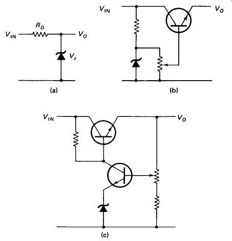
FIGURE 20-1 Representative discrete regulator circuits: (a) fixed voltage
zener; (b) zener with emitter follower; (c) error amplifier and series pass
transistor.
Load Regulation is the percent rise in dc output voltage when the load is removed.
The load is chosen to draw the maximum rated output current at maximum output voltage:
… where FL and NL stand for full load and no load, respectively.
Line Regulation is the factor by which the output voltage is stabilized against changes in input voltage. A line regulation of 20% means that a 10% line voltage change will produce only a 2% load-voltage change (10% X 20% - 2%).
... where O, I, H, and L stand for out, in, high, and low, respectively. For 117-V-input supplies, high and low inputs of 121 V and 110 V are recommended to produce a line change of 10%.
Output Impedance is the ratio of output-voltage change to output-current change for a fixed output setting and a changing load. This is already specified at low frequencies by load regulation, but at high frequencies the response time of the regulator may be too slow to maintain the low-frequency Z0.
Temperature Coefficient is the change in output voltage per degree temperature change. It may be expressed in mV / ° C or %-of-VQ/°C.
Alternatively, the total temperature stability may be specified for the entire operating range of temperatures, for example:
Temperature stability: 1.2%max, -25 to +83°C
20.2 GENERAL-PURPOSE IC REGULATORS
Quite a number of IC regulators are available, but their internal operation and external connections are generally similar. Figure 20-2 illustrates the basic regulator philosophy and shows the four sections included in most IC types.
The Voltage Reference is generally derived from a 7-V zener diode because the temperature coefficient is near zero at this voltage. The zener is fed by a transistor current source from the raw V + supply and is buffered by an emitter follower and compensating diode. Most regulators voltage divide the reference down to about 1.7 V before buffering to make it easier to obtain V_o below 7 V.
The Differential Amplifier compares a fraction of the regulated output voltage with the reference voltage and delivers an output signal which corrects for any difference. This dif amp is similar to the op amps of section 16 in its internal circuitry. It is powered by the unregulated input as +Vcc and ground as -Vcc, but the balanced nature of the dif-amp circuits allows it to reject the severe variations in this supply voltage.
The output voltage is selected by the ratio of the external voltage divider, Ra Rb. In Fig. 20-2, one fifth of V_O is fed back and compared to a 2.0-V reference, so V_O must equal 5 Vref or 10 V.
The Series Pass Transistor is integrated, but total package dissipation is limited to 0.5 to 0.8 W for most general-purpose regulators. The unregulated Vnw is required by the dif amp and pass transistor dive circuitry to be a minimum of 3.0 V above V0. Ripple and line-voltage changes will add to this difference, so that Vnw is likely to be 10 V average for V_O = 5 V. Maximum current is then P 0 5/ max = T -100 mA dif J
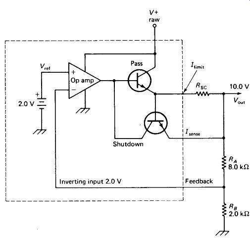
FIGURE 20-2 Representative IC voltage regulator showing Internal elements
and basic external circuit.
Higher currents must be handled by addition of an external series pass transistor with heat sink.
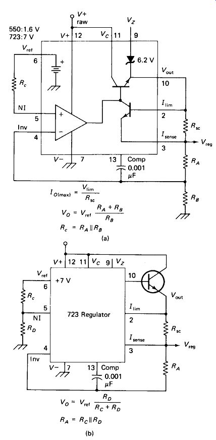
FIGURE 20-3 (a) Internal elements, pin Identification, and basic external
circuit for the 550 and 723 regulators in 14-pin DIP packages, (b) Placement
of Rc and RD for output voltages below 7 V with the 723 only, and placement
of external pass transistor for greater output current with 723 or 550.
The Current-Limit Transistor is integrated and is connected so that it can turn off the pass transistor by shorting its base to emitter. The current-limit transistor is activated when an external resistor Rsc (short circuit) in the output current path drops enough voltage to turn on its base-emitter junction.
Type 723 and 550 Regulators are pin-compatible, and are shown with their basic circuit in Fig. 20-3(a). The 550 outputs 1.6 V at pin 6, and the output of voltage divider RARB is compared to this reference. Rc is a compensating resistor to equalize the voltage drops caused by the bias currents of the two op-amp inputs.
Rb should be chosen somewhere near 5 k-Ohm and RA and Rc calculated from the formulas given.
The 723 outputs a 7-V reference, making ~ 7 V if = /?c = 0 and RB-*oo in the circuit of Fig. 20-3(a). Lower voltages are obtained by voltage dividing the reference down to the desired voltage and comparing this directly with Kreg, as shown in Fig. 20-3(b). Variable output can be obtained by using a pot for the upper arm of the voltage divider in either circuit. Enough fixed resistance should be used in series to avoid voltage demands and power dissipations beyond the rated limits of the IC.
Current Limiting is provided by selecting Rx to drop one VBE junction's voltage at maximum current. This voltage is about 0.6 V at 25°C, dropping to about 0.5 V at 100°C. Rsc can be replaced with a short circuit if minimum component count or minimum input/output voltage difference is desired and current limiting is not required.
High-Current Regulators can be built with the simple addition of a series pass transistor connected in a Darlington pair with the internal pass transistor, as shown in Fig. 20-3(b). Assuming a /?min of 20 for the power transistor and a drive current of 100 mA from the IC, the load current would be 2 A maximum.
The Vz pin and the internal 6.2-V zener are used in negative-voltage regulator circuits.
Type 300, 305A and 376 regulators are pin-compatible and are shown with their basic circuit in Fig. 20-4(a). All these types use a 1.7-V reference which is internally connected to the noninverting op-amp input, eliminating two package pins. The voltage-dividing resistors RA and RB should have a parallel resistance of about 2.2 k-Ohm to match the internal resistance driving the + input of the op amp.
The reference-defeat input, pin 5, actually accesses the + input of the op amp which is tied to the 1.7-V reference. This pin may be grounded to shut down the supply, or an external voltage may be forced upon it to vary the regulated output voltage.
The current-limit transistor is pre-biased in these ICs, reducing the RK shutdown voltage to about 0.35 V at 25° C, and about 0.30 V at 100° C.
Higher Output Currents can be obtained using the external Darlington-connected transistor, as shown in Fig. 20-3(b), but this increases the IN OUT difference requirement by one BE drop. This family of regulators has a boost output which will drive an external PNP pass transistor directly, as shown in Fig. 20-4(b). The medium-power PNP can in turn drive a high-power NPN, as shown in Fig. 20-4(c).
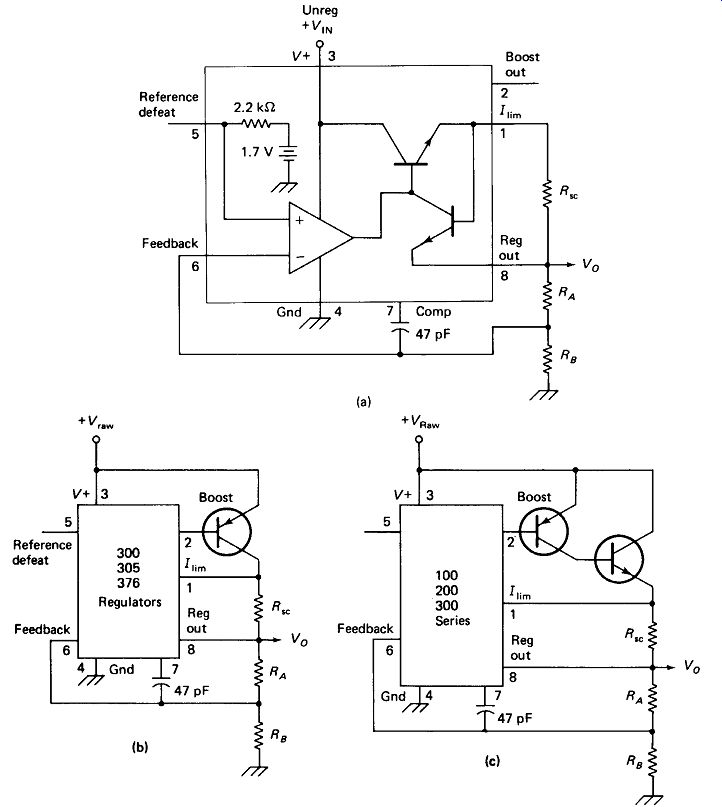
FIGURE 20-4 (a) Internal elements, pin identification, and basic external
circuit for the 300 and 305A regulators (0 to 70°C operating range) In 8-pin
round metal packages. The 200 and 205 (-2S C to 85 C) and the 100 and 105 (~55°C
to 12S°C) are similar. The 376 has the same pinout but comes in the low-cost
plastic 8-pin DIP package, (b) Adding an external PNP pass transistor, (c)
External NPN pass transistor.
20.3 FOLDBACK CURRENT LIMITING
In a regulated supply, even with current limiting, the power dissipation in the pass transistor can increase to many times the design limit if the load is short-circuited.
This is because the entire input voltage (not just the V_IN – V_OUT difference) now appears across the pass transistor. To prevent destruction of the regulator in case of a load short, foldback current limiting has been developed. Foldback limiting action decreases the current limit as the load resistance decreases, as shown in Fig. 20-5(a).
The Foldback Regulation Circuit is basically a Wheatstone bridge with the load resistance as one of its arms, as shown in Fig. 20-5(b). RK is quite a bit higher in value and drops more voltage than it does in the simple current-limit circuit, but with normal operating RL values this is compensated for by the drop across RE in the new voltage divider RERF, and the current-limit transistor is not turned on.
However, if RL drops to a short circuit, all of V_0 appears across RK, and most of this appears across the limit transistor. V_o is thus reduced to slightly more than sense- ant* the short-circuit current is much less than I_max because of the higher value of R_sc.
There is a trade-off here in that the input/output voltage difference requirement of the regulator circuit increases as the ratio of circuit increases. Roughly, folding 7SC back to 5 7max requires five V_sense drops across RK instead of one.
Foldback Circuits for Popular Regulator ICs are given in Fig. 20-6. The circuit for the type 550 deserves special comment because it eliminates the increased RK drop required with the other types and simplifies the foldback circuitry. This is possible because the 550 uses an integrated SCR instead of a transistor as the current-limiting element. Load currents in excess of the maximum will develop turn-on voltage of 0.6 V across Rsc which is fed to the SCR gate (current limit) and cathode (current sense) through Rc. Rc is necessary to prevent the SCR from being shorted by the low-resistance Rsc.
A value of about 4 k- ohm gives an 1 K about 15% of 7 max.
Rc can be dropped to 2 k-Ohm to give 7SC about 50% of 7m„.
This may be desirable, because once the SCR switches on, the load current must drop back below IK to turn it off again. If turn-on surges within the load circuitry exceed 7m.., and steady-state load current exceeds 7SC, the regulator will switch off and not come back on by itself.
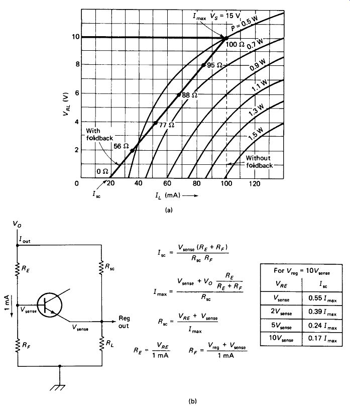
FIGURE 20-5 (a) Typical foldback current limiting: as R_L drops below 100 ohm,
load current decreases (diagonal line) instead of holding at I_max (dashed
line) as it does with conventional short-circuit limiting. Curved lines show
pass-transistor power dissipation for V_IN = 15 V. With foldback P_max 0.6
W at R_L = 88 ohm. Without foldback Pmax =1.5 W at RL = 0 ohm. (b) Basic foldback
circuit with analysis and design equations, and a chart for estimating I_sc.
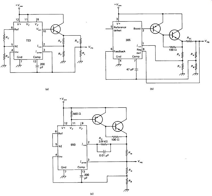
FIGURE 20-6 --- (c) Foldback current limiting circuits for the 723 regulator
(a) and the 300/305 regulators (b). Relevant equations are given in Fig. 20-5.
The 550 regulator achieves foldback with an internal SCR, hence the somewhat
simpler circuit (c). External pass transistors are shown since foldback is
most commonly used with higher-power regulators.
20.4 THREE-TERMINAL REGULATORS
Three-terminal regulators have an unregulated input pin, a regulated output pin, and a ground, which is usually the metal case for heat sinking. They are available in a variety of fixed voltages from ± 5 to ± 24 V, in the plastic TO-92 , the power tab TO-220, and the power TO-3 packages with output currents up to 3 A. Their low cost and extreme ease of application has brought them immense popularity in a very short time.
On-card regulation has become common since the advent of the three-terminal regulator. A heavy-current bus carrying unregulated voltage from a chassis-mounted supply's run past all the PC cards in an instrument with little regard for noise pickup or one drop. Each card then contains a small three-terminal regulator to supply its own circuitry, practically eliminating noise coupling via the supply lines.
Temperature Stability of the three-terminal regulators is markedly inferior to that of general-purpose regulators-output voltage changes of 1 to 2% over a 100° C temperature range are typical for three-terminal regulators, whereas general-purpose regulators have typical VQ changes of 0.1 or 0.15% over the same range. Guaranteed worst-case temperature stability is three to six times worse than these typical performance listings for general-purpose regulators, but few manufacturers will even put a guaranteed maximum temperature-stability specification on their three-terminal regulators.
Furthermore, a three-terminal regulator is more likely to experience wide temperature swings because it usually contains the series pass transistor. General purpose regulators can be kept at a relatively cool and even temperature by using an external pass transistor. In spite of all this, three-terminal regulators provide adequate stability for most logic and many op-amp power-supply requirements.
Most three-terminal regulators contain internal short-circuit current-limiting circuitry and will shut down automatically if the junction temperature rises above a safe value for any reason. Figure 20-7 shows some basic three-terminal regulator applications. The input capacitor is required for stability with some regulator types, and is especially recommended if the regulator is located more than a few inches from the power-supply filter capacitor. The output capacitor is seldom essential, but it does keep the output impedance low at high frequencies and improve the output purity when fast pulses of current (such as those produced by TTL) are drawn by the load.
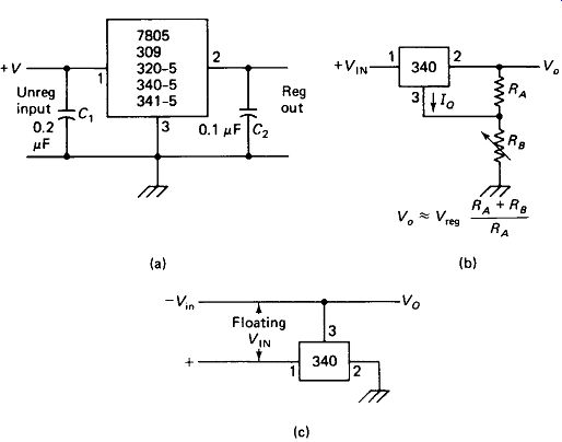
FIGURE 20-7 Three-terminal regulator circuits: (a) basic circuit: C, and C2
optional; (b) variable output voltage: keep Ira->Iq; (c) negative-supply
regulation with a positive regulator.
The Variable Regulator of Fig. 20-7(b) isolates ground pin 3 from the circuit ground, making heat sinking to the chassis a problem. Load regulation also suffers, because pin 3 delivers a quiescent current IQ, which is typically about 5 mA but which varies with temperature and input voltage. RA and RB should therefore be chosen to carry several times this current.
RB can be replaced by a zener diode to produce a simple regulated supply with V0 greater than the 24 V available in three-terminal regulators.
The negative regulator circuit of Fig. 20-7(c) requires that the input voltage not be referenced to ground (often an unreasonable demand in a large system), and it has its case terminal off circuit ground, presenting a heat-sinking problem. Negative regulators are available, but where only one low-current negative supply is required, Fig. 20-7(c) may make it unnecessary to inventory yet another IC type.
20.5 POWER INVERTERS AND CONVERTERS
A power supply operating at 60 Hz and requiring a 1-kg transformer and 1000 uF of filtering could, ideally at least, be built at 60 kHz with a 32-g transformer (1000 g/ V1000) and 1 uF of capacitance. High-frequency power supplies are understandably popular where space and weight must be conserved.
An Inverter is an oscillator driven from a dc source (typically a 12-V battery) feeding a transformer which outputs ac of the desired voltage. Figure 20-8(a) shows a simple 6-W inverter which operates at 60 kHz and was designed for a portable fluorescent lantern (fluorescent lamps boast light efficiencies of 12% compared to an incandescent , s 3%). The oscillator is an Armstrong type, and the sense of the 4-turn winding must be correct to give positive feedback.
The coils are wound on a 1-in. pot core.
Low-frequency inverters are used to produce 60 Hz at 120 V from 12 V dc.
Core saturation is more of a problem at low frequencies, so a push-pull oscillator is used to eliminate the dc current in the transformer primary. Frequency stability can be improved by driving the actual switching transistors from a separate low-power oscillator powered from the dc source.
A DC-to-DC Converter is simply an inverter with the ac output feeding a rectifier and filter. As noted above, the filter elements can be quite small if the oscillator frequency is high. Figure 20-8(b) shows a simple dc-to-dc converter using a push-pull oscillator.
Dc-to-dc converters can be regulated by feeding back a portion of the output to alter the bias point of the oscillator. Figure 20-8(c) shows a regulated dc-to-dc converter.
Flyback Power Supplies are step-down converters which operate directly from the rectified ac line voltage and provide line-to-load isolation by means of the high frequency pulse transformer. They are replacing conventional power supplies in many applications because of the size, weight, and cost advantages of eliminating the 60-Hz transformer. Figure 20-8(d) shows a flyback power supply designed to illustrate the principle as simply as possible. Dx and C, produce 165 V dc which is chopped at 30 kHz by Q3 and coupled via Tx to D4 which rectifies the kickback pulses produced when Q} turns off. The LED and photocell provide feedback which shortens the Q3 on-time if VQ rises. Section 5.6 explains the pulse transformer function in detail. R6 and D2 free R7 from charging C4, allowing sharp square waves at the collector of <22- Q prevents the disaster which would otherwise occur
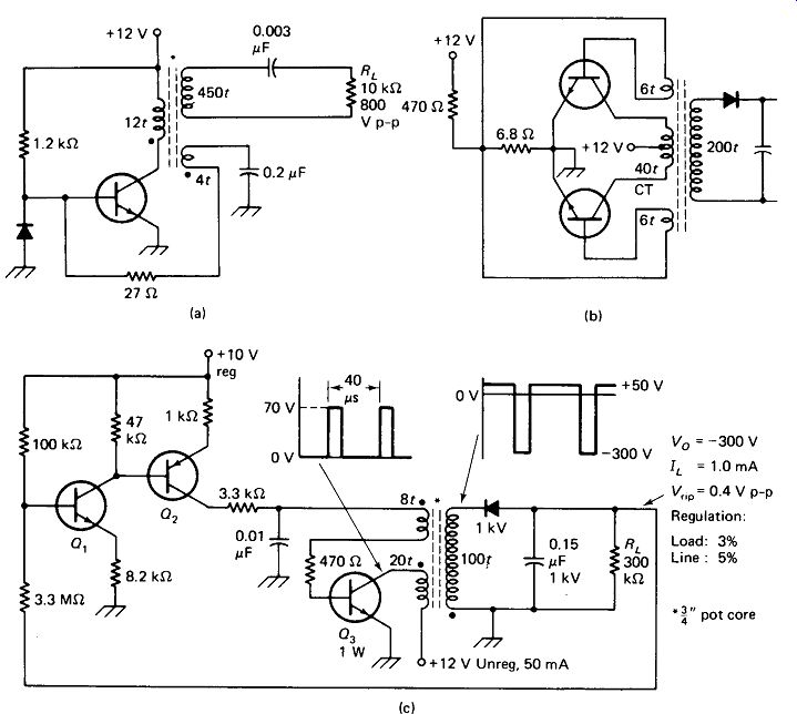
FIGURE 20-8 Inverters: (a) low-power Inverter; (b) high-power push-pull In
verter; (c) feedback-regulated dc-to-dc converter with half-wave rectifier
and simple capacitor filter.
Ripple: 60 mV rms, 30 kHz, at 220 mA Regulation: 0.4 V rise from 220 mA to 40 mA load Efficiency: 47% at 220 mA load Short-circuit toleration: 5 seconds Open-circuit toleration: Indefinite Transformer: Amidon PC3019-77 pot core; 70-turn primary, 7-turn secondary (d) ...
FIGURE 20-8 (d) Flyback supply eliminates 60-Hz transformer; (e) transformer
less dc-to-dc converter for supplying negative or boosted positive voltage
at low current.
... if multivibrator Qx - Q2 should "hang up" with Q3 turned on. More complex flyback supplies are capable of efficiencies above 80%.
A simple converter which can supply a negative or a boosted positive voltage at about 12 mA is shown in Fig. 20-8(e). The circuit uses no inductors, takes less than 10 cm2 of circuit board "real estate" and adds a parts cost of about $1.
The output current is enough to power five 741 op amps or a dozen 308s. Used on a + 5-V TTL line, it can produce enough bias for FET amplifiers or a CMOS 4016 analog switch. Note that Di and D2 should be moderately fast signal diodes, not conventional power-supply diodes.
20.6 SWITCHING REGULATORS
A switching regulator uses feedback to control the relative on and off times of a transistor, and thereby control the average current delivered to an inductor. This controls the average output voltage, which is filtered to pure dc by the inductor and an output capacitor. Figure 20-9(a) illustrates the basic principle. The diode is necessary to provide a discharge path for the inductor when the transistor turns off.
The inductor and capacitor need not be very large because the switching frequency is high. Typical values for a 1-A, 5-V supply are 0.5 mH, 200 uF, and 10 kHz. The diode, however, must be capable of turning off in less than a microsecond, so standard power rectifiers cannot be used. The filter capacitor must present a very low reactance and low equivalent series resistance at the switching frequency and its low-order harmonics. Low-quality electrolytics will degrade efficiency, reliability, and noise rejection.
Notice that there are no resistances in the circuit-the transistor and diode are essentially on-off switches, and L and C burn no power-so ideally the regulator is 100% efficient. Actual efficiencies up to 90% are practical. Linear regulators, operating from line voltages that vary ± 10%, or in extreme cases ± 15% using 5%-tolerance components, are hard-pressed to achieve a worst-case efficiency of 70%. Low-voltage supplies, such as the common + 5-V TTL supply, are lucky to exceed 50% efficiency considering the extra drops for external pass transistors and foldback circuitry. Remember that for 100 W of output, 90% efficiency produces 11 W of dissipation in the regulator, while 70% produces 43 W and 50% produces 100 W of wasted power.
Switching-Regulator Drawbacks: The fast switching of high currents generates noise spikes which can interfere with other parts of the system via stray capacitive or inductive coupling or the input or output supply lines. Shielding and filtering are often required. The consequences of a failure, particularly a shorted switching transistor, can be rather serious, so protective circuitry at the output and input is a good investment. Switching regulators are also slow to adjust to rapid changes in output current, making them less desirable than linear types where the load current contains fast pulses.
Step-Down Regulator Action is best understood by looking closely at the representative circuit of Fig. 20-9(a). It is easy to see that a 100% duty cycle (Q, always on) would produce Vo ~ IN> neglecting losses. Lower duty cycles will produce a rectangular waveform, as shown at the base of Q}, because Z), switches on as soon as Qt switches off. The average value of this waveform is:
(20-4)
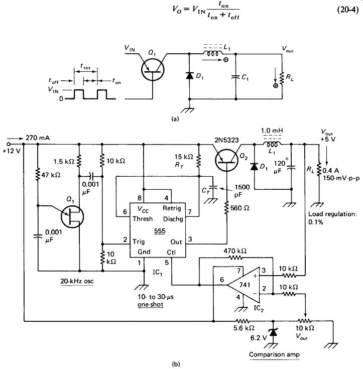
FIGURE 20-9 Step-down switching regulator: (a) representative circuit; (b)
practical circuit with Q, oscillator, IC-, pulse-width-modulated one-shot,
driven by IC2. which compares output with zener reference.
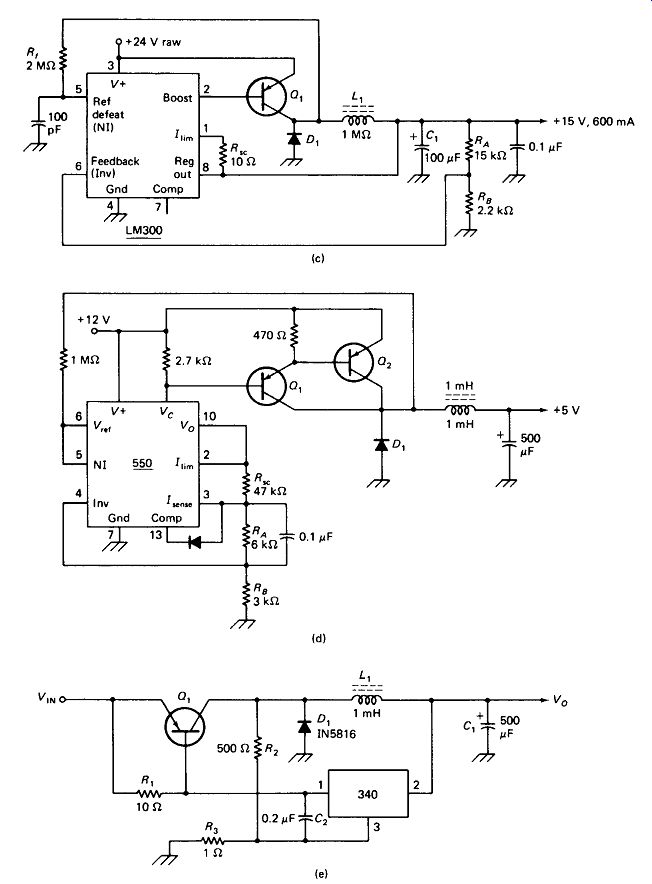
FIGURE 20-9 Step-down regulators may use the 300/305/376 IC (c), the 550/723
IC (d), or a three-terminal regulator (e) in a self-oscillating mode.
The LC filter transforms the pulses into dc of their average value. Load current has no primary effect on the duty cycle required. It is not necessary or even desirable that VQ be as near as possible to KIN, as it is with linear regulators. A ViN of 50 V with V_o of 5 V can be achieved with no loss of efficiency.
The time constant of the inductor and load resistance should be at least twice the off time of the switching transistor:
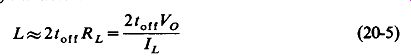
(20-5)
Notice that large load currents require smaller inductors. Peak inductor current may be 1.5 times the load current, and core saturation must be avoided, however.
The filter capacitor can be determined by considering L, and C, as a voltage divider with IN (p-p square wave) across XL and VQ (p-p ripple) across Xc. There is considerable error in treating the input rectangular waveform as though it were a sine wave, but the approximation is usually adequate, and reduces to ...
(20-6)
... where / is the switching frequency.
Figure 20-9(b) shows a complete switching regulator using a UJT oscillator to drive a 555 IC pulse generator. The width of the pulses is varied by the output of a 741 op amp whose input compares VQ with a fraction of the voltage obtained from a reference diode.
Figure 20-9(c) shows a simpler regulator using a type-300 regulator IC in a self-oscillating mode. The 2-MB resistor provides positive feedback to the noninverting op-amp input, switching Q1 on with a snap action. This part of the circuit is actually an op-amp Schmitt trigger, with Rf controlling the dead zone. When Q, turns on, VQ rises, but relatively slowly due to L, and C,. This rise is fed back to the inverting op-amp input via RA and RB, and Qx snaps off after the hysteresis is overcome. Some ripple at VQ is necessary to operate the Schmitt trigger. Lowering Rf will increase the ripple (hysteresis) and decrease the switching frequency. A second LC section can be added to remove this ripple. Figure 20-9(d) shows a similar self-switching regulator using a type-550 IC.
A simple switching regulator using a three-terminal regulator IC is shown in Fig. 20-9(e). Qx is turned on by the inrush of current from .N to pin 1 of the IC. A small part of FIN is applied to reference pin 3 of the IC via voltage divider R2R3 when the collector of Qx turns on. This decreases the voltage between reference pin 1 and output pin 2, ensuring that the IC will continue to conduct heavily until VQ rises by 1/500 of K1N. Once VQ does rise by this amount, the IC shuts off, turning 0, off. C, then discharges through RL until V_o is again low enough to cause the IC to conduct. Output ripple is in excess of 1 /500 of and a second LC section may be needed to bring it to an acceptable level. Lowering R3 reduces ripple but also increases switching frequency while lowering switching speed, resulting in reduced power efficiency.
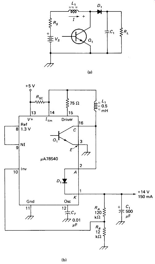
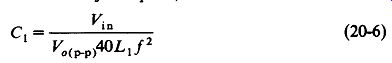
FIGURE 20-10 Step-up switching regulator: (a) representative circuit; (b)
practical circuit using 78S4QIC with integrated power transistor, fast power
diode, and oscillator.
A Step-Up Regulator is shown in principle in Fig. 20-10(a), with a practical version given in Fig. 20- 10(b). Q1 is turned on for a small fraction of a time constant Lx/Rs. When Q1 is turned off, L1 generates a kickback voltage which adds to Vs and is applied through D1 to C1 and the load. There is no hard-and-fast limit to the voltage-step-up-ratio- V_o can be several times Vs.
The practical step-up regulator uses an IC specifically designed for switching regulation. It contains an oscillator, a fast diode and switching transistor capable of handling 1.5 A, and a second op amp in addition to a 1.3-V reference and comparison amplifier.
An Inverting Regulator is shown in principle and in practice in Fig. 20-11 (a) and (b), respectively. When Q1 is turned on, conventional current flows down through L1 as shown. When Qx is turned off, this current continues to flow, producing a kickback voltage which charges C1 through D1.
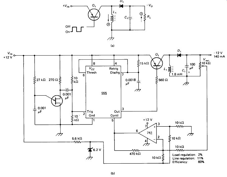
FIGURE 20-11 Voltage-inverting regulator: (a) representative circuit; (b)
practical circuit.