7.1 SEMICONDUCTOR MATERIALS AND JUNCTIONS
A diode is a two-terminal device whose current response to an applied voltage is different for the two possible directions of applied voltage. The original vacuum tube diodes were used almost exclusively as ac-to-dc converters, but today's semiconductor diodes have properties and varieties which invite a much wider range of applications. A few moments spent in studying the nature of semiconductor materials may bring some order to the bewildering range of characteristics exhibited by the different diode types, since the internal structure is similar for most of them.
Intrinsic Semiconductors: The electronic properties of a material are determined primarily by the outer layer of electrons (called the valence shell) of its atoms.
Conductors have many mobile electrons which are free to flow from atom to atom, while insulators have a place for each electron, and each electron remains in its place. Semiconductors have four electrons in the valence shell, although there is room for eight. This allows the atoms to pack together with four neighbors around each one, sharing electrons so that each inner atom has all eight spaces filled.
Figure 7-1 gives a two-dimensional representation of this crystal-lattice structure, although a. box packed with marbles would give a better idea of the actual three-dimensional form.
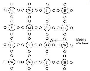
FIGURE 7-1 Representation of a silicon crystal with N-type impurity (mobile
electrons).
Intrinsic (perfectly pure) semiconductor material is nonconductive at low temperatures, since each electron is held in a fixed space. Heat, which is essentially vibration of the atoms, can cause some of the valence electrons to break out of the lattice, thus rendering the materials conductive.
TV-doped Semiconductors: Notice that the silicon crystal lattice represented in Fig. 7-1 is not perfectly pure.
One of the silicon atoms has been replaced by arsenic, which has five electrons in its valence shell. There is no fixed place in the crystal lattice for this electron. It is mobile, and is termed a negative charge carrier. We say that the silicon is TV-doped, rather than intrinsic.
Two points should be noted concerning this impurity doping. First, the introduction of negative charge carriers does not mean that the material is given a negative charge, since the arsenic atoms bring an extra proton for each extra electron. Second, impurity concentrations of a few parts per million are all that is required to transform the material from an insulator to a fairly good conductor.
P-doped Semiconductors: An equally effective method for rendering a crystal lattice conductive is P doping, in which an impurity such as boron, which has three electrons in its valence shell, is added. The lattice now has a vacant spot or hole, as shown in Fig. 7-2. If a positive voltage were applied at the light side of this lattice, an electron from the second column may be attracted to fill in the third column, leaving a new hole in the second column. The hole has thus moved away from the positive voltage, as a positively charged particle would. We term the hole a positive charge carrier.
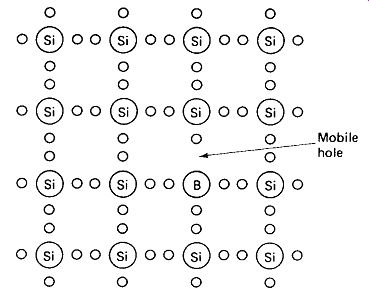
FIGURE 7-2 Representation of a silicon crystal with P- type impurities (mobile
holes).
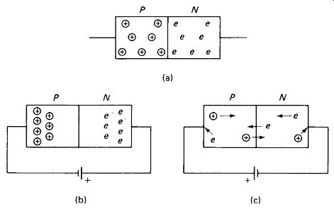
FIGURE 7-3 (a) P-N junction or semiconductor diode, (b) Reverse bias forms
an insulative depletion zone around the junction, (c) Forward bias attracts
charge carriers across the junction.
PN-Junction Behavior: When P- and TV-type materials are joined, a basic diode is formed. With no applied voltage, the charge carriers are distributed essentially as shown in Fig. 7-3(a). Notice that only the mobile charge carriers are shown. The lattice electrons and the inner atoms are not shown because they are immobile.
If an external voltage is applied as shown in Fig. 7-3(b), the charge carriers will be attracted toward the potential of opposite sign, leaving the region around the P-N junction depleted of all charge carriers. This depletion zone is insulative and no current can flow in this direction. The diode is said to be reverse-biased.
The opposite voltage polarity (positive to P, negative to N) results in charge carriers being pulled across the junction, and current flows easily, as depicted in Fig. 7-3(c). The diode is now said to be forward-biased.
7.2 FORWARD-VOLTAGE CHARACTERISTICS
Threshold Voltage: We have seen that a semiconductor diode will not conduct under reverse bias but will conduct readily under forward bias. It must not be assumed that any arbitrarily small forward voltage makes the diode appear as a perfect short circuit, however. There is a tendency for the electron charge carriers near the junction to migrate across to fill the holes on the other side. To the extent that this occurs, a negative charge appears on the P side, with a corresponding positive charge on the N side of the junction. These minority charge carriers produce a potential across the junction which must be overcome by the forward bias before current can begin to flow. This turn-on or threshold voltage is quite different for different materials, as shown in Fig. 7-4(a). For silicon diodes, which are by far the most common type, the forward current rises by an approximate factor of 10 for each 80-mV increase in voltage. This produces a linear curve on semilog paper, as in Fig. 7-4(b). For a typical 1-A silicon diode, the following table provides a good estimate of V versus I:
Small-signal diodes may show 0.1 V greater drop, and heavy-current rectifiers may show 0.1 V less. In addition, there will be a small amount of ordinary resistance in series with the diode because of the semiconductor material and connecting-lead resistivity. This resistance may reach 1 ohm or so for small-signal diodes, but is much smaller for power diodes.
Variations in Forward Voltage: Diodes with identical type numbers may commonly show voltage drops which are different by 0.1 V. Put another way, identical type diodes wired in parallel may carry forward currents that differ by a factor of 10. Parallel connection of diodes to increase current capacity is therefore not recommended. Matched diodes, which were formed side by side from the same wafer of silicon, are available for applications where it is absolutely necessary that the forward voltage-versus-current curves track. The diodes in commercially available bridge-rectifier packs track typically to better than 10 mV.
Temperature Variations: The forward voltage across a silicon diode may be expected to decrease by typically 0.1 V as operating temperature rises from 25° C to 100°C. For diode applications requiring closely tracking voltages, matched diodes physically mounted on a common heat sink should be employed.
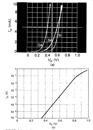
FIGURE 7-4 (a) Threshold voltage differs for different diode materials,
(b) Straight-line curve for silicon diode on semilog paper.
Diode Current Ratings: Diodes are generally rated for their maximum permissible forward current (average half-wave rectified to a resistive load, which is nearly the same as the dc rating). This limitation is imposed by the power product, P= IV, where V is the forward-voltage drop, and is a function of the physical size and heat sinking of the diode. The basic rating applies at or below the specified free-air temperature, and must be reduced according to a chart or derating formula if higher operating temperatures are anticipated. As a rule of thumb when manufacturers' ratings are unknown, lead-mounted diodes should be limited to case temperatures of 100°C, and stud-mounted types should be limited to 150°C. Paints and stick-on labels are available which melt or change color at specific temperatures to test case temperatures. Lead-mounted diodes can be kept slightly cooler if their leads are kept short (2 or 3 mm) and soldered to a relatively large-area binding post or copper pad.
Surge Currents: Diodes are capable of handling extremely large nonrepetitive pulses of current if their duration is too short to allow the diode junction to overheat. Surge current ratings 10 to 20 times 7av are typical for 8.3-ms pulses (half-cycle on a 60-Hz line), increasing to 50 to 100 times 7av for 2-ms pulses. Such pulses are commonly encountered when a power supply is turned on and the filter capacitors charge up from zero. The amplitude of the pulse can be calculated from the effective transformer resistance.
EXAMPLE 7-1 Determine the peak surge current for the diode in Fig. 7-5. Also estimate the number of cycles until the current settles to normal.
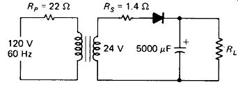
FIGURE 7-5 Surge current is limited only by transformer winding resistance
at turn-on (Example 7-1).
Solution
The primary resistance reflected to the secondary is Rref = n1RP = (j)2 X 22= 0.9 ohm
The total charging resistance, peak voltage, and peak current are
Rt= R r + R* = 0.9+ 1.4 = 2.3 ohm VpV = 24 x 1.
41 =34Vpk
The charging time constant gives an estimate of surge-time requirements.
r = RC = 2.3 0 x 5000 uF = 11.5 ms
This is considerably more than one half-cycle, so the manufacturer's chart would be consulted to find a diode with a 15-A surge rating for 2 cycles' duration.
7.3 REVERSE-VOLTAGE CHARACTERISTICS
Leakage Current: Silicon diodes are remarkably insulative in the reverse direction, but some leakage current does flow, as shown in Fig. 7-6. Notice that the leakage increases markedly with temperature.
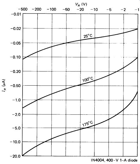
FIGURE 7-6 Diode reverse leakage current increases at high temperatures.
Reverse-Voltage Breakdown: If the reverse voltage across a silicon diode is increased, the charge carriers for the leakage current will be accelerated to higher velocities as they cross the junction. Some of these charge carriers will collide with atoms in the crystal lattice, and eventually a voltage will be reached which gives them enough energy to knock electrons loose from the valence band of the parent atom. The resulting hole-electron pair contributes to greater leakage and may itself be accelerated sufficiently to dislodge more electrons, and so on in an avalanche of conduction, as shown in Fig. 7-7.
This avalanche condition is not in itself destructive, but two factors dictate that extreme care be taken to limit the current that is permitted to flow in the reverse direction. First, the current necessary to produce destructive temperatures is much less at the relatively high avalanche voltages than at low forward voltages.
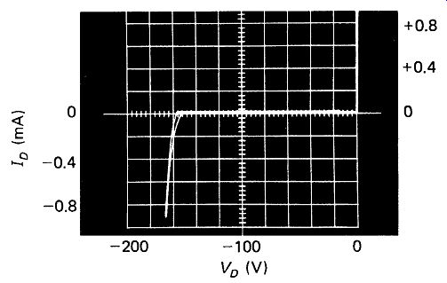
FIGURE 7-7 Beyond the rated PRV (peak-reverse voltage) of a diode an avalanche
point will be encountered at which the diode begins to conduct heavily.
A diode carrying 1A at 1V forward dissipates 1 W, but at reverse avalanche of - 500 V it need only carry 2 mA to dissipate the same power. Second, although it is possible to control the doping of the P-N junction so that all portions go into avalanche at the same voltage, not all manufacturers do so. Diodes without controlled avalanche characteristics may experience hot spots which seriously reduce their power-handling capability in the reverse direction. As might be expected, high-current diodes with their large junction areas are more troubled by hot spots than low-current diodes.
Diodes in series: Low-current diodes (1 A or less) operating from a 60-Hz sine-wave line may generally be connected in series to obtain higher peak-reverse voltage (PRV) ratings. The calculated PRV should always be multiplied by a safety factor of at least 2, since the ac line is notorious for occasional transient spikes of high voltage. The diode having the highest back resistance will, of course, hog the first of the rising reverse voltage, but this is not a problem since it will simply go into nondestructive avalanche when its limit is reached, throwing the remaining voltage to the other diodes in the string.
With high-current diodes and with high frequency or square-wave input voltages, the fact that diodes cannot turn off instantly becomes important, and shunting capacitors are required to protect the fast diode in the string, as shown in the next section.
7.4 DYNAMIC CHARACTERISTICS
Reverse Recovery Time: A diode that has been conducting in the forward direction has free charge carriers all along its length, in a density directly proportional to the forward current. To become nonconducting, all these charge carriers must be cleared from the junction area, leaving a depletion zone. This takes time, and the diode is capable of conducting in the reverse direction until it is accomplished. Figure 7-8 shows a test circuit and the recovery times measured for several power and signal diodes. Figure 7-9 shows that the recovery times of two identical-type-number 3-A diodes may differ by more than 3 us.
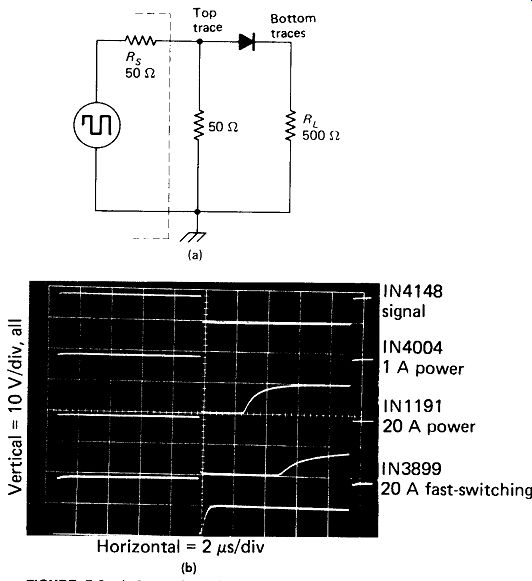
FIGURE 7-8 A forward-conducting diode requires a certain time t, to return
to the nonconducting state: (a) test circuit; (b) the storage time t, is
greater for higher-current diodes, although fast-recovery power diodes are
available for a price.
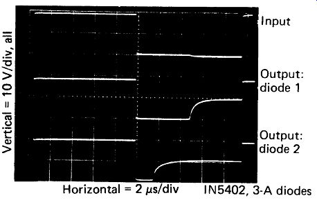
FIGURE 7-9 Identical diode types may have widely different storage times.
Fast Switching of series Diodes: If one diode in a series string turns off 1 jus faster than any of the others, and if the applied voltage is a square wave, so that it rises to full reverse value instantly, the fast diode will go into avalanche and will experience a current limited only by the series resistance of the source. The resulting instantaneous diode power can be alarmingly high. For 60-Hz sine-wave rectification, the reverse voltage rise is gradual and the diodes have ample time to turn off, but for switching inverters that have rise times on the order of 1 /is and frequencies of several kHz, it may be necessary to slow the voltage rise across the fast diode with a capacitor, as shown in the following example.
EXAMPLE 7-2
In the circuit of Fig. 7-10, it is possible that the diodes may have reverse recovery times which differ by as much as 1 jus. The inverter provides a 1500 V p-p 60-Hz square wave through a series resistance (transformer secondary plus reflected primary) of 100 0. The diodes are rated at 1 A, 1.0 V forward, maximum.
Determine whether shunt capacitors are needed for the diodes, and if so, calculate their value.
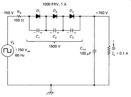
FIGURE 7-10 Fast-switching high-voltage diodes in series may have capacitors
(C1-C3) placed across them to give all diodes a chance to turn off before
applying reverse voltage to them (Examples 7-2 and 7-3).
Solution
Assume that the third diode has turned off while the first two remain on for l /is.
The filter capacitor maintains + 750 V at the right end of the diode string. With the source internally applying -750 V, we have a total of 1500 V across Rs, two turned-on diodes, and a diode in avalanche at 1000 V. The voltage and current for Rs and then the instantaneous power for Z)3 are calculated:
The average power due to the forward current is about 0.1 A X 1.0 V or 0.1 W, so the 1-W limit of the diode is not being exceeded. However, in the absence of any assurances that the diodes possess controlled avalanche characteristics, we should anticipate hot spots and be reluctant to accept a safety factor less than 10. Determination of the shunt-capacitor value follows.
With D1 and D2 conducting, we will ensure that R, does not charge C3 to more than one-third of the reverse voltage across the diode string during the 1 μs before D1 and D2 turn on. This maintains the PRV safety factor of two. In general:
C = n- delta t_s/R
... where n is the number of diodes and A/, is the difference in storage times (7-1).
Of course, equal-value capacitors are normally used for C1 and C2 since, in a production situation, it is not known just which of the three diodes is the fastest.
Note that these capacitors function as RC charging-rate limiters, and are not ac voltage dividers as they appear at first to be. Relatively broad-tolerance ceramic types are therefore quite acceptable.
Diode reverse-recovery characteristics also have consequences for the power transformer if the positive-to-negative voltage transition is faster than the diode turn-off time. For the few microseconds while the diodes are reverse-biased but still conductive, the transformer resistance Rs receives the sum of the filter capacitor voltage and the reverse transformer voltage. The average power dissipation in the transformer can be significant at high frequencies.
EXAMPLE 7-3
In the circuit of Fig. 7-10, the diodes may have reverse recovery times of 5 u.s.
Calculate the added power dissipation in the transformer due to reverse-current pulses.
Solution
= 22,500 W pk
The disadvantage of using overly large shunt capacitors is now apparent, as they add to the reverse conduction time:
A final consequence of shunt capacitors across series rectifiers is the added ripple across the filter capacitor when the charge stored in their series combination is dumped into C_filt at the start of each conduction cycle. The peak-to-peak ripple thus produced is:
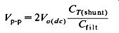
(7-2)
For the example of Fig. 7-10, this amounts to only 0.15 V p-p, but for light current supplies with low filter-capacitor values, the effect could be severe.
A few summary comments regarding diode storage time may now be in order:
1. Silicon power rectifiers (50-A rating or so) may be expected to remain conductive for typically 20 us after they are switched from forward to reverse bias. As long as the switching transition time (square wave) is several times longer than this (say, 50 ps), or the sine-wave frequency produces transitions similarly slow (say, 10 kHz maximum), reverse conduction should be no problem. One-ampere diodes can be expected to be 5 or 10 times faster than this, while silicon signal diodes have recovery times on the order of 1 to 100 ns.
2. If the switching time cannot be reduced by LC or RC circuit arrangements, fast-switching diodes are available for a price. For example, the 1N3913 switches 30 A in 100 ns, but costs about $5.
3. High-voltage rectifiers can be placed in series to obtain higher PRV, but they are vulnerable to high avalanche currents if subjected to fast turn-offs.
Generous safety factors (PRV rating two or three times actual expected) and line-transient suppressors (thyrector diodes or RC networks) are recommended to reduce the possibility of failure. Shunt capacitors are recommended for series high-current diodes where inductive loads or square-wave switching are involved. Such capacitors are not particularly helpful where the input is 60-Hz sine wave and the load is noninductive.
Forward Recovery Time: Diode turn-on time is typically at least an order of magnitude less than turn-off time, and the effects are generally not harmful in any case. In fact, forward turn-on is often masked by the charge stored in the diode's junction capacitance. This capacitance may be on the order of 10 pF for 1-A or 100 pF for 50-A diodes. It is charged on the reverse half-cycle, and this potential is added to the source during the first portion of the conduction cycle, as shown in Fig. 7-11.
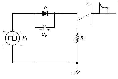
FIGURE 7-11 Charge stored on the diode junction capacitance CD in the reverse
half-cycle may add to Vs on the forward half-cycle, producing an overshoot
on the square wave output.
7.5 ALTERNATIVES TO THE SILICON DIODE
Although the silicon diode captures more than 90% of the market for rectifiers, there are applications where other types are used.
Schottky Barrier or Hot- Carrier Diodes: These diodes employ a silicon-to-metal junction to produce a rectifier with a forward drop typically half that of comparable silicon P-N-junction diodes, with virtually zero reverse-recovery time. Power Schottky’s are available that will handle 40 A forward with a drop of 0.5 V, so they are an attractive alternative for minimizing power waste in low-voltage/high-current supplies. Their zero turn-off time makes them ideal for high-frequency inverters and switching regulators. In this application, maximum frequency is limited, not by storage time, but by junction capacitance which commonly exceeds 0.001 uF for power Schottkys at low reverse voltages. Hot-carrier (Schottky) rectifiers also have relatively high reverse-leakage currents (as much as 0.01 of the rated IF at maximum operating temperature) and are limited, at present, to reverse voltages less than 100 V. Figure 7-12 shows the forward and reverse characteristics of a low-power Schottky diode at 25 and 150°C.
Schottky signal diodes are widely employed as microwave detectors and mixers because of their extremely fast turn-off characteristics. Additionally, a whole subfamily of logic elements (the 74S00 series) has been developed using integrated Schottky diodes to improve the switching speed of conventional TTL circuits.
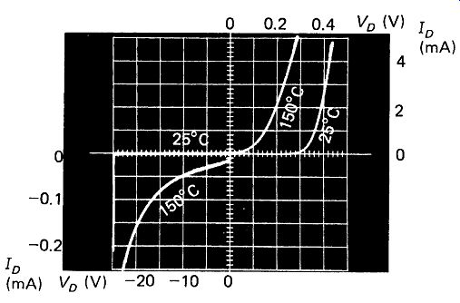
FIGURE 7-12 The Schottky diode has a lower turn-on voltage than the silicon
diode, but leakage is severe at high temperatures.
Germanium Diodes: Like silicon, germanium is an element with four electrons in its valence shell, and germanium /V/V junctions can be formed in a similar manner.
Germanium diodes start to turn on at a lower voltage than silicon, but the advantage becomes less important at high currents. More important is the tempera ture limitation: germanium devices generally have a maximum junction tempera ture specification from 80 to 110°C, compared to a specification of 170 to 200°C maximum for silicon devices. Silicon diodes can, therefore, handle higher currents for a given package size, even though they drop slightly more voltage. Reverse leakage current and storage time are also notably inferior to comparable silicon units.
Germanium point-contact diodes have been widely used as detectors in receiver circuits because of their low cost and low turn-on voltage. At currents above a few milliamperes, however, the resistance of the internal contact causes a voltage drop greater than that of silicon.
Selenium Rectifiers were popular in the late 1950s, but are seldom seen today. They have a limited life proportional to voltage and current stress, and they smell horrible when overheated. They drop about 1 V forward per cell, but each cell has a reverse-voltage limit of only a few tens of volts, making a stack of cells mandatory for high-voltage rectification.
7.6 ZENER AND AVALANCHE DIODES
Avalanche Diodes: The avalanche phenomenon, wherein high-speed charge carriers collide with and dislodge valence electrons, has been described in Section 7.3.
The result is the rapid transition of the reverse-biased diode from non-conduction to
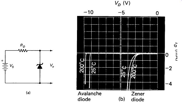
FIGURE 7-13 (a) Basic zener (or avalanche) diode circuit.
Changes in V8 are taken by RD, leaving V„ constant, (b) Avalanche and zener characteristics showing opposite temperature coefficients.
full conduction at the avalanche voltage. By changing the doping level and junction width, the reverse breakdown voltage can be controlled and brought down as low as 6 to 8 V. Such a diode, supplied from a higher-voltage source through a suitable dropping resistor, as in Fig. 7-13, will maintain a nearly constant voltage across its terminals, regardless of variations in the voltage source.
Avalanche Noise: The inherent violence of the collisions involved in the avalanche mode of conduction results in a good deal of random electron motion, which shows up as noise across the diode. This noise increases slightly at lower avalanche currents, but becomes extremely severe at the threshold of conduction, as seen in Fig. 7-14. The energy of the avalanche noise covers a wide frequency range, but it is the higher-frequency components which are most likely to cause problems by stray-capacitive coupling to other circuits. These can be filtered to an acceptable level by simply placing a 0.1-jnF capacitor across the diode. If elimination of the low-frequency noise is required, the zener will have to be followed with an RC filter, and the poorer load regulation due to the added source resistance will have to be tolerated.
Zener Diodes: The avalanche phenomenon does not occur below about 6 V, but it is possible to construct a regulator diode with similar behavior based on a different principle. If the P-N junction is made extremely narrow, the voltage gradient (volts/cm) across the depletion zone will be high enough to pull some electrons out of their valence bands, even though the total voltage is only on the order of 5 V. This high-field breakdown is properly termed zener conduction, and is shown in Fig. 7-13 in comparison to avalanche conduction. Notice that the zener knee (start of conduction) is much less abrupt than the avalanche knee. Note also that the zener voltage varies somewhat more with current than does the avalanche voltage, as indicated by the steeper vertical slope of the avalanche-mode curve.
Noise generated by the zener diode is typically an order of magnitude less than for the avalanche diode.
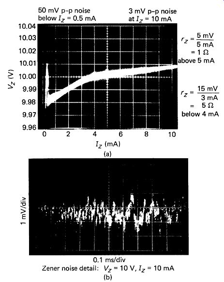
FIGURE 7-14 Dc flowing through an avalanche diode produces random noise
which becomes more severe at the threshold of conduction.
Temperature Coefficients: The distinction between avalanche and zener diodes is not often made by manufacturers, who tend to sell them both under the names breakdown diode, regulator diode, or zener diode. Besides the better voltage regulation of the avalanche diode and the lower noise of the zener diode, there is, however, a distinct difference in the effect of temperature on breakdown voltage for the two devices. Thermal agitation of the crystal lattice makes it easier for the high field to pull loose some electrons, so zener breakdown voltage decreases at higher temperatures (negative temperature coefficient). However, such agitation makes it difficult for an electron to find a long-enough clear path to acquire the velocity necessary to initiate avalanche collisions, so avalanche breakdown voltage increases at higher temperatures (positive temperature coefficient). The voltage change involved can easily be as high at 5 to 10% for 0 to 100°C temperature shifts.
Regulator diodes in the 6 to 7-V range exhibit a near-zero temperature coefficient because of a balance between the zener and avalanche effects.
Since the forward turn-on voltage of an ordinary silicon diode decreases with temperature, it is possible to produce a higher-voltage zero-temperature-coefficient regulator by placing an avalanche diode in series back to back with an ordinary diode having an equal but opposite temperature coefficient. They can be recognized by the fact that they do not conduct at 0.6 V in the "forward" or non-breakdown direction as uncompensated regulator diodes do.
Self-heating within the diode is usually the major cause of wide temperature variations, so it follows that better voltage regulation can be obtained by operating the diode at the lowest possible current levels. Cascading one regulator circuit after another will keep the current to the second diode nearly constant in spite of source voltage changes, thus improving output-voltage stability.
Dynamic Resistance of Regulator Diodes: Increasing the current through a zener or avalanche diode does produce a slight voltage increase across the device, as illustrated in Fig. 7-15. This AK/A/ ratio is the dynamic resistance of the device, Zz7. or RZT, which is useful in calculating its response to ripple or to changes in input voltage and load current.
Quality avalanche diodes operating at 500 mW can be expected to have RZT in ohms equal to or less than the numerical voltage rating (i.e., RZT of 10 B for a 10-V 500-mW diode). Zener diodes typically have a dynamic resistance several times lower than given by this rule of thumb. Dynamic impedance can be expected to be roughly inversely proportional to dc current. For example, a 10-V diode at 50 mA dc might exhibit R ZT = 10 ohm, rising to 100 ohm at 5 mA dc. A power avalanche diode operating at 10 V, 500 mA, would be expected to have RZT = 1ohm.
There is so much variation in this parameter, however, that it is wise to trust nothing but the manufacturer's guaranteed specifications on RZT, where they are available.
Voltage-Regulating Circuits: The basic regulator circuit of Fig. 7-13 provides ripple reduction and stabilization against line-voltage and load-current changes. Its limitations are (1) fixed output voltage, (2) limited output current, (3) temperature sensitivity, and (4) avalanche noise. Transistor or IC amplifier circuits can be used to remedy the first two problems. Temperature effects are best combated by limiting diode current to reduce self-heating to an absolute minimum. Tempera ture-compensated regulator diodes may also be employed. Noise can be limited with a 0.1-uF filter or by using the lower-voltage zener diodes.
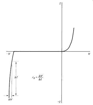
FIGURE 7-15 Dynamic resistance (resistance to changes in voltage) is given
by the slope of the curve AV/AI.
EXAMPLE 7-4
In the circuit of Fig. 7-16, an unregulated 18-V source containing 0.2-V p-p ripple feeds a regulator diode with the following parameters:
~ 10 V r ambient
= 25° C Pzmu=iw TC = 7 mV/
° C 7]nax
= 175° C /?zr= 7 iimax at 25 mA
The load current of 30 mA may drop to zero.
(a) Find RD to operate the diode at 250 mW.
(b) Find the minimum input voltage that will maintain Iz" 1 mA, and the output ripple at this point.
(c) Find the maximum input voltage that will keep Pz below maximum ratings, and the ripple at this point.
(d) Find the dc output voltage change from (b) to (c).
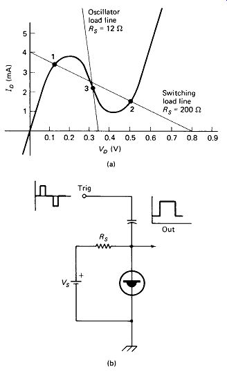
FIGURE 7-18 Zener regulator circuit with load resistance (Example 7-4).
Solution
(a) For a diode power of 0.25 W at 10 V, Iz is 25 mA:
R 18 ~ 10 _ Iz + h 25 mA + 30 mA
(b) If Iz drops to 1 mA:
Vrd = Uz + 'l)Rd = 31 mA X 145 - 4.5 V Kn
=Vz+ Vrd = 10 + 4.5 - 14.5 V
The value of RZT at 1 mA is estimated as 25 times that given at 25 mA:
Rzt= 25 x 7 - 175 0
Voltage division of 0.2 V across R D and the parallel combination of R2 and R1 gives the output ripple:
Rl = T = ° 333 f IL 30 mA Rl II Rz = 333|| 175= 1150
= Q2 T4T5TT5 = ®-®f8VP-P (c)
For a diode power of 1 W at 10 V, /z is 100 mA.
The worst case occurs when load current drops to zero:
Vrd = IzRd = 100 mA X 145 - 14.5 V Vin
= Vz + Vrd = 10 + 14.5 = 2AS V
Rzt is estimated as j of the 7 ohm, specified at 25 mA, or 1.75 0. RL is negligible in calculating V0:
V° = Q2 T45TT75 ™ t.f®24 V P"P
(d) From near-zero power at (b) to full-rated power at (c), the diode will experience a temperature rise from near 25 ° C to 175°C, or 150°C.
AK= rCAr=7mV/°Cx 150°C= 1.05 V
The foregoing analysis should make it clear that it is wise to avoid low zener currents in the interest of better ripple reduction and to avoid wide swings in zener current in the interest of better voltage regulation.
Thyrectors and Varistors: A variety of bidirectional voltage-clamping devices are available for suppressing transient overvoltages across ac or dc supply lines or sensitive semiconductors. The devices may consist of back-to-back avalanche diodes, or selenium diodes, or ceramic-composition materials, and may be marketed as thyrectors, varistors, VDRs, or other trade names. They are available with limiting voltages from ± 10 to over ± 1000 V. Energy ratings in joules are specified rather than power ratings in watts, because the transients they are expected to suppress are too brief to allow heat dissipation to the environment.
EXAMPLE 7-5
It is desired to suppress transients on a 120-V ac line which may be as high as 2000 V pk through a 150-ohm source impedance and may last as long as 100 /is.
Choose an appropriate thyrector.
Solution The peak ac line voltage may approach 190 V on a nominal 120-V-rms line, and the thyrector absolutely must not conduct under this voltage. A 250-V thyrector is chosen, giving a 30% safety margin.
V 2000 - 250 R 150 W = Pt = IVt = 11.7 X 250 X 0.707 X 100 /is = 0.2 J J-J, 250-V unit would be selected.
EXAMPLE 7-6
Select a thyrector to protect the switching transistor in Fig. 7-17 from inductive transients produced by the relay coil. Switching speed may be as high as 10 pulses per second.
Solution
The thyrector voltage must be greater than 24 V and less than 65 V. A rating of 40 V is chosen. The energy expended by the coil at each pulse is:
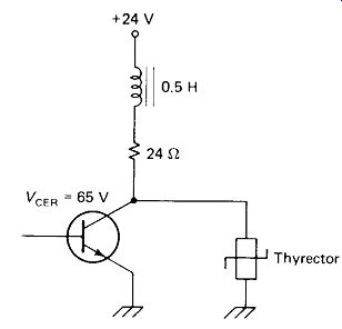
FIGURE 7-17 A thyrector diode prevents voltage surges Wh could be damaging
to other semiconductor
The average power may be as high as p _ W _
0.25 J/pulse X 10 pulse _ 2 5 yv ~~~ t Ts "
Part of this energy is delivered to the coil's internal resistance, so the ratings given above are somewhat conservative for the thyrector.
7.7 TUNNEL DIODES
The tunnel or Esaki diode is a two-terminal device capable of switching, oscillating, and amplifying at low power levels into the gigahertz region. Its unique characteristic curve, shown in Fig. 7-18(a), cannot be accounted for by traditional conceptions of atomic structure, and must be explained by the newer and more complex theories of quantum mechanics. The devices are formed as silicon, germanium, or gallium arsenide P-N junctions that are very heavily doped to produce extremely narrow depletion-zone barriers. The unexpected currents that were observed were facetiously said to be due to electrons tunneling under the barrier, since they supposedly did not have enough energy to "climb over" it.
A Switching Circuit is produced by biasing the diode from a relatively high-voltage source through a high-value resistance, as shown in Fig. 7-18(b). Two stable points (1 and 2) are thus available, and the diode can be switched between them by externally applied pulses.
An Oscillator is produced by biasing the diode from a low-voltage source through a low-value resistor, so that only one bias point (3) is possible. Since the source voltage required is generally 0.2 to 0.3 V, it is most convenient to use a voltage divider having the required Thevenin-equivalent voltage and resistance, as shown in Fig. 7-19(a). The parallel-tuned circuit L and C determines the frequency of oscillation and must be wired with an absolute minimum of stray inductance and capacitance if VHF self-oscillation is to be avoided. Oscillation below 1 MHz will be difficult to control in any case.
FIGURE 7-18 (a) A tunnel diode can be biased either as a switch or an oscillator,
(b) Tunnel-diode switch circuit.
FIGURE 7-19 (a) Tunnel-diode oscillator circuit, (b) Damped wave decreasing
as energy is lost in circuit resistance, steady wave in an ideal lossless
LC circuit, and increasing wave with energy supplied by negative resistance.
The oscillation mechanism is most interesting. It is well understood that the oscillations in an LC tuned circuit will die away due to the inherent resistive losses of the components unless energy is added in the proper phase from the outside.
Ideal L and C components would have zero resistance and would allow the oscillations to sustain themselves indefinitely, as in Fig. 7-19(b). The tunnel diode has a negative resistance at the oscillator bias point, since increasing voltage causes decreasing current. A tunnel diode suitably biased can thus be placed in series with a tuned circuit to cancel its positive resistance, allowing the ideal of perpetual oscillation to be realized. The amplitude of the oscillation is limited by the range of the negative-resistance region of the diode, which generally lies between 0.1 and 0.4 V.
Back Diode: Tunnel diodes with peak-point currents of only a few uA are called tunnel rectifiers or back diodes, and are used to rectify signals as low as 20 mV pk.
The conductive direction is the "reverse" direction by conventional diode terminology, and the nonconductive direction is " forward" direction. The terms "back direction" and "tunnel direction," respectively, are recommended to avoid confusion. Of course, if signals above about 0.4 V pk are encountered, the tunnel rectifier will begin to conduct in both directions, limiting the rectifier output to 0.5 V dc. A Schottky diode can be used to improve the rectifier's response at higher voltages, as shown in Fig. 7-20.
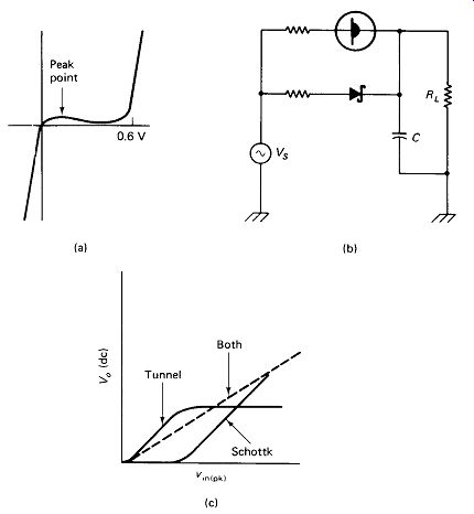
FIGURE 7-20 (a) Back-diode curves, (b) Low-level detector using back diode
for 0-to-100-mV range and Schottky diode for range above 100 mV. (c) Output
of detector circuit.
7.8 VARACTOR DIODES
As was shown in Fig. 7-3(b), a reverse-biased diode consists of two conductive N and P-doped zones, separated by an insulative depletion zone. These regions form, respectively, the plates and dielectric of a capacitor. Increasing the reverse bias widens the depletion zone, effectively increasing the plate separation and lowering the capacitance. Thus any P-N junction diode is a voltage-variable capacitor.
Typical power diodes have capacitances of a few tens of picofarads at low reverse bias. Diodes manufactured to exploit this variable-capacitance effect are called varactors and are available with maximum capacitance from a few picofarads into the 1000-pF range. Capacitance tolerance of ± 10% for a specified reverse voltage is common. Changes on the order of + 1 or + 2% for a 25°C temperature rise may be expected.
Maximum-to-minimum capacitance ratios may be as low as 2:1 or as high as 20:1. Device Q (reciprocal of dissipation factor) is generally a few hundred at low reverse bias, increasing to several thousand at high reverse bias.
Used as part of a tuned circuit in a radio-frequency oscillator, varactors can be fed by audio voltages to produce frequency modulation, or by dc feedback voltages to produce automatic frequency control or automatic color control in radio and TV circuits. As replacements for mechanical variable capacitors, they are smaller, more rugged, less affected by vibration, and often less expensive.
Figure 7-21 shows a typical voltage-variable tuned circuit and the K-versus-C curve for a representative varactor. Notice that maximum specified capacitance is achieved at - 0.3 V across the varactor, dictating a rather small rf signal (0.6 V p-p) to avoid forward-biasing the diode on positive signal swings. For a 6-V-p-p signal, the control voltage would have to be held greater than -3 V, making the maximum usable varactor capacitance 40 pF.
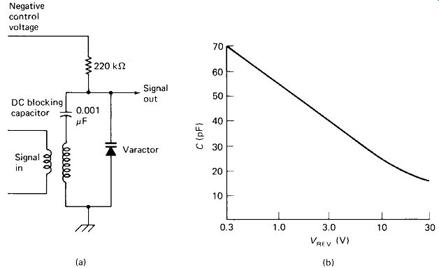
FIGURE 7-21 (a) Circuit diagram for varying the frequency of a tuned circuit
with a dc voltage to a varactor diode, (b) Typical C versus VR curve for
a varactor diode.
Varactor Multipliers: Power varactor diodes are useful for producing several watts of output power at frequencies in the l-to-3-GHz range, where power transistors are unavailable or prohibitively expensive. Efficiencies on the order of 60 to 70% are obtainable in the frequency doubler or tripler mode, so that 10 W at 500 MHz from a conventional transistor rf amplifier can be used to produce 6 W at 1500 MHz.
The principle of operation of the varactor multiplier is easy to grasp if the following basic facts are understood.
1. Nonlinear elements tend to distort sine-wave signals.
2. Distorted sine waves are really nothing more than fundamental sine waves with harmonic sine-wave components added (Fourier's theorem).
3. A diode, ideally at least, burns no power since it is always fully on (zero voltage) or fully off (zero current).
4. A capacitor burns no power, since it is a reactance.
5. A varactor is nonlinear, both as a diode and as a voltage-variable reactance.
Figure 7-22 shows an elementary varactor doubler. The input network is tuned to the fundamental while the outputs are tuned to the second harmonic. The 100-k ohm resistor keeps the varactor biased so that it is always driven just slightly into conduction by the input signal positive peaks.
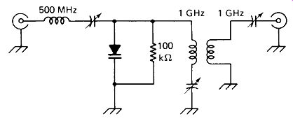
FIGURE 7-22 Circuit diagram for a frequency doubler using a varactor diode
to generate harmonics.
7.9 LIGHT-EMITTING DIODES
In a forward-biased P-N diode, hole-electron pairs are constantly being formed and recombining. The recombination process releases energy, which for certain materials is manifested as visible light. Although red is by far the most common, LEDs can produce yellow, green and infrared radiation.
Forward turn-on voltage for the most popular gallium-arsenide LEDs varies between 1.0 and 2.0 V. Forward current requirements vary with size and desired intensity, but generally fall between 2 and 20 mA. Reverse voltage must generally be limited to 4 V or less to prevent reverse breakdown.
Actual light power output from an LED is less than 1% of the electrical power input at 25°C. This efficiency nearly doubles for each 25°C reduction in temperature, and halves for each 25 °C increase. At any given temperature, light-output intensity varies directly and quite linearly with forward current.
Response speed for LEDs is quite good, 0.1-us rise times being typical.
Laser Diodes: Common light sources actually produce a confused jumble of radiation at many frequencies and in random phase. Laser light, by comparison, is generated at a single frequency and phase. The two types of radiation are termed incoherent and coherent, respectively. "Static" and "snow" are examples of in coherent signals in the RF range, as opposed to a radio-transmitter carrier which is coherent. By giving special attention to the precision of the optical surfaces during manufacture, LEDs can be produced which generate coherent light at forward currents in the range 10 to 100 A. The heating effect of such high currents makes desirable a pulsed mode of operation with a duty cycle on the order of a fraction of 1% to avoid overheating. Cooling the LED junction can reduce the required current for laser action by approximately half for each 50°C reduction.