8.1 BASIC TRANSISTOR ACTION
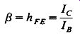
The original transistor is sometimes called a bipolar or bi-junction transistor (BJT), to distinguish it from the several other types of "transistors" which were developed subsequently. Its essential feature is current gain: a small input current from base to emitter acts to control a much larger current from collector to emitter. The existence of a dc collector supply capable of delivering the required current is assumed. The ratio of collector current to base current is the current gain, beta, of the transistor:
(8-1)
Notice that, to a good approximation at least, collector current does not depend upon collector-emitter voltage, but only on base current.
Transistors are available in two polarities. Assuming that the emitter is at ground, the NPN operates with positive potentials at its base and collector, and PNP operates with negative potentials, as shown in Fig. 8-1.
FIGURE 8-1 The basic transistor action is to use a small base current to control a large collector current.
FIGURE 8-2 Ideal (a) and real (b) transistor characteristic curves. Some
of the limitations are exaggerated in (b) for clarity.
Characteristic Curves: The ideal transistor would be completely described by its current gain, Ic = Beta I_B. Real transistors place many restrictions on this idealism, however, and the art of using transistors is largely the art of learning to operate within these restrictions. A graph of collector current versus collector-emitter voltage for a series of fixed-base-current values turns out to be remarkably helpful in assessing and visualizing the limitations of a transistor. Such graphs are called collector characteristic curves and can be displayed on a cathode-ray tube using a curve tracer or an inexpensive curve tracer adaptor for a conventional oscilloscope.
Figure 8-2(a) shows an idealized set of characteristic curves for a transistor having a /? of 100. Notice that Ic is 100 times IB, anywhere on the curves, regardless of collector-emitter voltage. Figure 8-2(b) shows, in exaggerated form, several of the limitations of a real transistor. Beta is not constant, but varies with Ic and with VCE. There is a minimum voltage, called V_CE(sat), below which the transistor's collector current falls off rapidly and beta becomes meaningless. There is a maximum voltage, called V_CE(sus), above which the collector current increases almost without limit. In addition, Ic does increase slightly with VCE, a condition that becomes quite severe at high Ic and low V_CE. The next several sections will detail these and other properties of real transistors.
8.2 VARIATIONS IN BETA
Unit-to-Unit Variations: Transistor-specification sheets generally include the minimum and maximum guaranteed beta for a specified collector current and voltage at a temperature of 25° C.
Minimum-beta specs may range as low as 10 for high-current types to several hundred for high-gain types. Guaranteed maximum beta may be less than 100 for some types and in excess of 1000 for others, but often no upper limit is specified. It is common to find that the range of possible betas for the same type of transistor spans a factor of 10. A factor-of-2 span (at a fixed current, voltage, and temperature) can be achieved by purchasing specially selected lots, but this is expensive, and the replacement problem causes premature baldness among field-service technicians.
Common practice is to design circuits that are independent of beta, as long as it exceeds some critical minimum value. The designer or service technician then need only select a transistor type such that any unit will have this minimum beta at any current, voltage, temperature, and frequency encountered in service.
Variations with Temperature: Transistor beta typically increases by 50 to 100% as temperature rises from 25°C to the maximum operating temperature (approximately 175°C for silicon or 85°C for germanium at the semiconductor junction).
By the same token, a decrease to 50 to 70% of specified beta may be expected at very low temperatures ( - 55°C). Figure 8-3 documents the effect for two popular silicon transistors.
Variations with Collector Current: A transistor with a beta of 100 at Ic = 10 mA may have a beta of only 50 at Ic = 0.1 mA, as illustrated in Fig. 8-3. Even more drastic drops in beta are evident at collector currents near the maximum ratings of the transistor. Specifications for minimum beta are often given only for a collector current near the peak of the Beta versus Ic curve, and it must not be assumed that this minimum applies at significantly higher or lower currents.
Dynamic or AC Beta: When used as ac-signal amplifiers,
transistors translate small changes in base current to large changes in collector current. The relevant property is not then total Ic over total IB, but change in Ic over change in IB. Thus we define ac beta:
(8-2)
Except at very high values of Ic or very low values of Vce, ac beta hfe and dc beta
hFE seldom differ by more than 20%, and we do not usually bother to make a distinction between their numerical values. Figure 8-4 shows how ac beta drops drastically where the characteristic curves are pinched together.
FIGURE 8-3 Variation of Beta with I_c for typical low-power (a) and high-power (b) transistors.
8.3 COLLECTOR SATURATION VOLTAGE
When a transistor's collector current is limited not by the transistor itself (I_c = beta I_B) but by the collector supply voltage and resistance (fc= Vcc/Rc), the transistor is said to be fully turned on, or saturated. Another way of saying this is that an increase in IB will not result in further increase in Ic. The ideal transistor would have Vce = 0 at saturation. Actual transistors will have C£ from 0.1 V or less at collector currents of a few milliamperes up to 2 V and more at collector currents above 10 A.
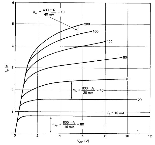
FIGURE 8-4 Variation of ac beta (h„) with collector current for a typical
power transistor.
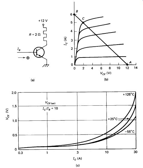
FIGURE 8-5 (a) Transistor used to switch a heating element, (b) Load line
for circuit (a) showing the minimum 2-V drop due to collector saturation
voltage
VcE(ttt)- (C) Variation of VCEf„,; with lc and temperature.
Low-saturation voltage at high collector current is important in a switching transistor, because most of the transistor's power is burned in this state. Figure 8-5 shows a transistor switching in a 2-ohm heating element on a 12-V supply, and the characteristic curves of the transistor. With the transistor turned off, no collector current flows and the full 12 V appears at the collector (point A). No power is burned in this state since there is no current. If the transistor could be made a perfect short from collector to emitter, the full 12 V would appear across R. The collector current would be:
= 6A
This is represented as point B on the curves. All possible conditions of voltage and current for this circuit must lie on straight line AB. Because of the saturation characteristics of the transistor, any reasonable base current leaves VCE = 2 V and the remaining 10 V across R. Thus:
= 5A
= 50
= 10W
The subscript Q is used to identify a transistor, every reasonable letter having been used elsewhere before their invention.
The definition of saturation voltage is somewhat arbitrary since continued increases in base current can always produce slight decreases in V_CE(sat).
Most manufacturers use IB = 0.1 Ic and specify minimum V_CE(sat) at some stated collector current. KCE(sat) generally remains uniformly low until a critical collector current is reached, whereupon it increases rapidly, as shown in Fig. 8-5. Increases in temperature generally cause increases in FC£.(sat), an effect that becomes more pronounced and more critical at high collector currents, again as illustrated in Fig. 8-5.
8.4 COLLECTOR-VOLTAGE LIMITS
Transistor collector-voltage limits may be given by any of more than a dozen different symbols. This section will attempt to sort out the confusion.
Off-State Limits: One method of setting the specification views the transistor not as an active device but as a pair of diodes. The avalanche voltage of the collector-base diode, with the remaining (emitter) lead left open, is then specified as the " collector-voltage limit "
VCBO, This specification method produces higher numbers than the active-state methods given below, and is therefore fairly popular among manufacturers seeking a competitive edge. A proliferation of specifications has grown up which supposedly involve both junctions, but in fact short the base to emitter (VCES), effectively short it with a low-value resistor (VCER), or even reverse bias it (VCEV). All these specifications produce numbers that are about equal to VCBO, and all are likewise misleadingly high.
To be sure, a transistor with a solidly turned-off base-emitter junction can withstand the collector-emitter voltages of these specifications, but at these voltages there is no smooth transition from the turned-off to the conducting state, as indicated by the dotted "negative-resistance" line in Fig. 8-6. Attempts to traverse the negative-resistance region may result in self-oscillation at some high frequency determined by stray inductance and capacitance. If the transistor and circuit parameters are tightly controlled, exceptionally fast on-off switching can be achieved by operating the transistor across this region in what is termed the avalanche mode.
Active-State Limits: The most commonly specified transistor voltage limit is K:eo> the collector-emitter breakdown voltage with the base left open. This specification is typically about one-half of VCBO or VCES for any given transistor.
These breakdown ratings may be given by various manufacturers as VCEO(m»x)>
K(Br)ceo> 0r BVceo<
With the same meaning. A smooth transition from off to on state can generally be made if the supply voltage is not greater than VCEO, although slight negative resistance and nonlinearity may be encountered at the high-voltage end if a low-value load resistance is used.
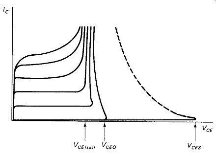
FIGURE 8-6 Three collector limiting voltages shown in approximate proportion:
VCEfsu,; with base forward-biased, VCEO with base open, and VCES with base
shorted to emitter.
The highest voltage for which a transistor's characteristics are a reasonable replica of the ideal curves of Fig. 8-2(a) is termed the sustaining voltage. To be complete, the collector current and the base-emitter conditions should be specified.
The most commonly given sustaining voltage specs for low collector currents are FC£0(sus) with the base open, or VCer(sus) with the base effectively shorted to the emitter. VCE0(sus) is typically about 80 to 90% of VCEO- VCer(su«) may be about equal to or slightly greater than VCEO, Notice from Fig. 8-6 that at higher currents the ideal shape of the curves gives way at less than half of Vceo- High-current voltage limits are, unfortunately, almost never specified by transistor manufacturers.
Choosing Transistor Voltage Limits: If a transistor is used strictly as a switch and the base is grounded or reverse biased at turn off, it will withstand a collector supply equal to VCBO, VCes> cer> 0r cev a" of which are about equal. If the base is left undamped to ground, the transistor will withstand a collector voltage ceo If linear operation with a resistive load is required, the collector-supply limit should be VCEO(sus).
If the load contains inductance, such as a choke, transformer, solenoid coil, or motor, the transistor collector-voltage rating should be double the supply voltage, since the inductive voltage adds to the supply voltage during turn-off.
Published voltage limits generally apply at 25°C and should be reduced to 75% of this value to cover maximum operating temperatures. Depending upon the reliability level required, an additional safety factor (up to a factor of 2) is recommended.
Secondary Breakdown, also called second breakdown, is a destructive effect caused by localized heating at certain points along the base-emitter junction. The problem is most often noticed when a high-voltage/high-current load is switched off rapidly, especially if the load is inductive and the pulsing is repetitive.
Since the edges of the junction turn off more quickly than the center portion, excessive current concentration and overheating occur in the center. Figure 8-7 shows a representative safe-operating-area curve for avoiding secondary breakdown.
As long as all portions of the load line lie within the specified area for the pulse conditions given, the manufacturer guarantees that secondary breakdown will not occur.
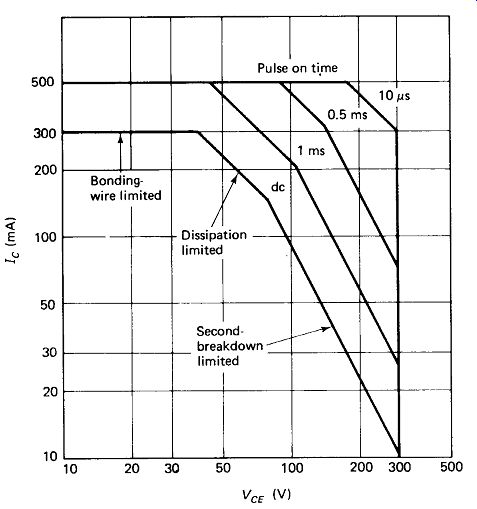
FIGURE 8-7 Safe operating areas for a high-voltage transistor.
8.5 POWER-DISSIPATION LIMITS
The power generated within a transistor is nearly equal to C CE> since base current and voltage are usually negligible by comparison. Maximum-power specifications for low-power types generally assume free-air mounting at room temperature (TA = 25°C). A second specification may be given assuming that the case is attached to a heat sink held at room temperature (Tc = 25 ° C). Derating factors are then given (in mW/°C) for ambient temperatures above 25°C. It is assumed that, if the transistor is attached to a heat sink, the temperature of the sink is not significantly raised by the heating effect of the transistor.
Heat Sinking: Power transistors are often rated for power dissipation at a case temperature of 25°C, with derating factors for higher temperatures. It is generally not practical to neglect the temperature rise of the heat sink for transistors dissipating more than 1 W, however. Figure 8-8 shows how the power limit can be calculated from the maximum junction temperature and the thermal resistance from junction to ambient. Heat, expressed in watts, can be visualized as flowing through thermal resistance, producing a temperature drop across the resistance.
This is analogous to electrical current flowing through a resistance, producing a voltage drop. The higher the temperature differential, the greater the heat flow. The higher the thermal resistance, the less the heat flow.
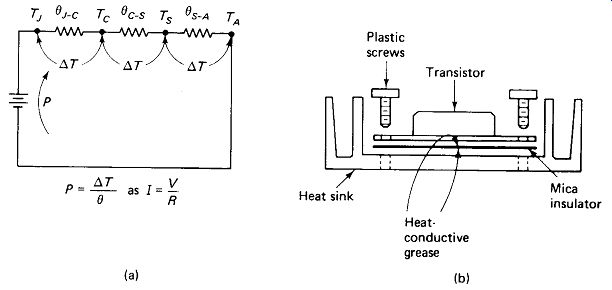
FIGURE 8-8 (a) Thermal power (watts) flows through thermal resistance (S),
producing a temperature differential AT. The subscripts refer to junction,
case, sink, and ambient. The use of an electric-circuit schematic to represent
the process is common, (b) Typical mounting of a transistor to a heat sink
with insulation of the transistor case.
Power-transistor specifications usually include maximum junction temperature Tj and junction-to-case thermal resistance 9j_c.
Manufacturers of heat-sinking devices supply case-to-sink resistance 0C_S figures for their insulators and sink-to-air resistance 0S_A for their heat sinks. Calculation of maximum power is then quite straightforward.
EXAMPLE 8-1
A transistor has a maximum junction temperature of 180°C and 0/_c of 1.5°C/W.
It is mounted through a 0.5°C/W insulator to a 3.5°C/W heat sink. Ambient temperature is 55°C maximum. Find the transistor power limit.
Solution
Total resistance and temperature differential are found first:
In many cases the transistor will be mounted directly to the heat sink, making insulator resistance 0C_ S equal to zero. Some data sheets may specify the maximum case temperature Tc, rather than 7}, thus eliminating junction-to-case resistance 0j_ c from consideration. If both of these possibilities are true, Ohm’s law for thermal circuits reduces to:
ATc_ a , , P = ~ JL M " s-A
This illustrates that the law is valid for part of the series circuit as well as for the entire circuit.
Thermal Resistance: In cases where a transistor is operated without a heat sink, the following table of case-to-air resistances may be used:
Case Style
9c_y, (°C/W) TO-92 (plastic) 350- 200 TO-18 (mini TO-5) 300 TO-5 (standard) 150 T0-60 (stud mount) 70 TO-66 (mini TO-3) 60 T0-220 (power tab) 50 TO-3 (standard power) 30 TO-36 (1 j" round) 25
Heat-sink insulators of the mica, plastic, or anodized-aluminum type typically have a thermal resistance of 0.35°C in.^2/W (2.3°C-cm^2/W). Note that smaller areas produce higher resistances, so

(8-4)
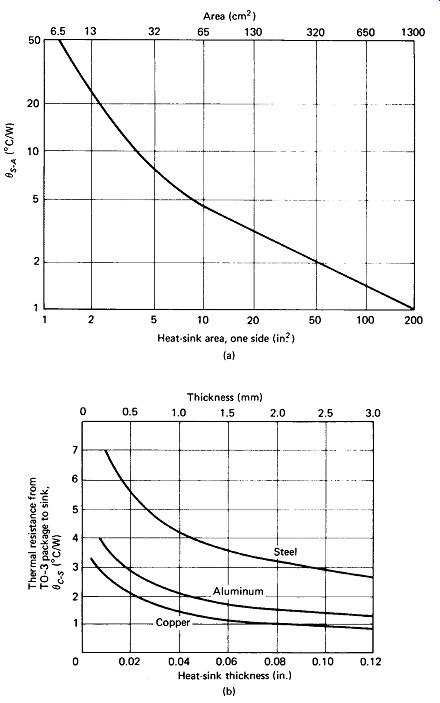
FIGURE 8-9 (a) Thermal resistance versus total surface area for a square
sheet painted black and mounted vertically in free air. (b) Thermal resistance
versus sheet-metal thickness for a TO-3 case mounted to a flat metal surface.
Silicon grease or a similar heat-sink compound should be applied to all the mating surfaces to prevent air spaces and consequent higher thermal resistance.
Commercial heat sinks are often more expensive than the transistor they serve, so it is common to use a simple square of aluminum or a part of the chassis or cabinet as a heat sink. The graph of Fig. 8-9(a) can be used to estimate the thermal resistance of such sinks. The values are approximate for a square aluminum sheet mounted vertically in free air to encourage convection and painted matte black to maximize radiation. For other conditions the following factors apply:
Condition | Multiply theta by
Horizontal mounting 1.3
Shiny aluminum surface 1.5
Fan-forced cooling 0.5-0.3
Figure 8-9(b) gives the thermal resistance due to heat conduction from TO-3 package to a thin metal plate. For manufactured heat sinks the metal is always chosen thick enough to make this resistance negligible compared to the dissipation resistance of Fig. 8-9(a). Where a chassis or cabinet is used to sink tens of watts of power, however, inability of the thin metal to conduct the heat to its large surface area may be the limiting factor.
Thermal Time Constant: If a transistor is pulsed with a large amount of power, the thermal capacitance of the case will absorb energy and prevent overheating of the junction for a short time until thermal equilibrium is reached. If it is assumed that the junction temperature rises according to the familiar time-constant curve of Fig. 8-10, the maximum power for a given pulse length can be readily determined, as shown in the example below. One should retain a healthy respect for the kind of trouble he is courting by operating beyond the steady-state limits, however. A relatively-harmless failure in a low-power drive circuit should never be allowed to avalanche into a catastrophic failure in the output stage, load, or power supply.
Note also that the cooling time constant is somewhat longer than the heating time constant. If the interval between pulses is not at least three cooling time constants, allowance must be made for cumulative heating.
EXAMPLE 8-2
A TO-3 package transistor is rated Tj = 200°C, 0y_c = 1.5°C/W and V_CE(sat) < 2.0 V at Ic= 15 A. How long can a 15-A on pulse be sustained without a heat sink, and how closely may such pulses be spaced?
Solution
Assuming that TA = 50°C and referring back to the table of thermal case resistance:
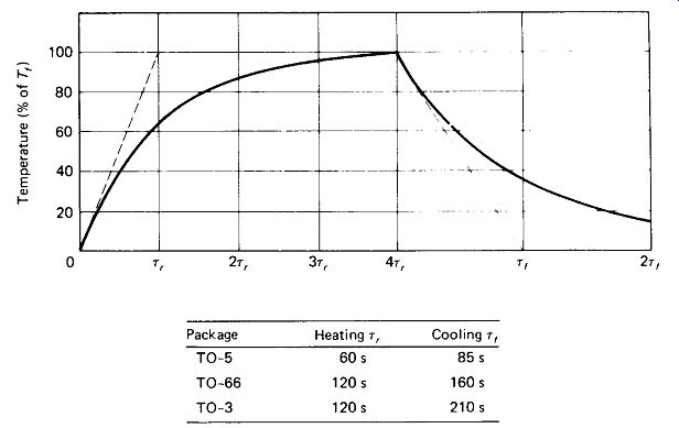
FIGURE 8-10 Heating and cooling time constants for various transistor packages.
The pulse power is considerably greater than this:
Ppulse
= IV = 15X2 = 30 W
The 30-W temperature-rise curve must be stopped at 16% of its full value to avoid overheating. The time-constant curve is in the linear region giving about 0.16rr as the time for this rise. Using the rr value from Fig. 8-10:
To allow a safety margin, an 8-s limit would be specified.
Cooling time between pulses should be
t_ min = 3T/(coo1) = 3 X 210 s = 10 min
A thermally-operated shutdown circuit is strongly advised to protect against driver failure.
Average Power: When a transistor or other device receives pulses of power at a regular rate much faster than its thermal time constant, it is common practice to compute the average power and treat it in the same manner as dc. Thus a 10-W pulse of 1-s duration recurring every 5 s would be treated as a 2-W continuous dissipation.
When a transistor is switched from the on to the off state, the power product IV becomes very large during the transition. If the switching rate is low, the time spent in transition will be negligible, and this will present no problem. However, at high switching rates the power burned in transition when averaged may far exceed the saturation-state power. Exact calculation of transition power is well nigh impossible, since switching waveshapes are usually irregular and stray capacitance and inductance causes time lags between voltage and current waveforms. However, for the idealized transition waveform of Fig. 8-11, the average power during transition time t r can be shown to be
P=IV/6 (8-5)
When a transistor is operated not as a switch but as a linear amplifier, calculation of transistor dissipation from the IV product at the collector is impractical for all but the simplest waveforms. Neither can average or true rms voltage at the collector be used, since the transistor does not have a constant value of resistance. The power input to the entire amplifier stage can be easily determined, however, since the Vcc supply is usually dc. The power output to the load is also fairly easy to measure if the load is resistive. Neglecting losses in any coils, transformers, and resistors in the collector circuit, the transistor power is simply the difference between the two, as illustrated in Fig. 8-12.
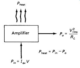
FIGURE 8-12 Relationship of dc Input power, signal output power, and heat
dissipation in an amplifier.
8.6 COLLECTOR LEAKAGE CURRENTS
In normal operation, a transistor’s collector-base junction is reverse-biased. A small leakage current flows, nevertheless, and is termed the collector cutoff current with emitter open, ICBO This leakage current must be stated for a specific voltage and junction temperature.
The transistor treats this leakage current entering the base just as it would a current injected through the base lead-it amplifies it by beta in the collector.
Thus the collector-emitter current, with the base left open (termed ICEO), is beta times Icbo. Remember that beta at such low currents may be quite a bit less than beta at normal current levels.
In germanium transistors ICEO is often a noticeable addition to the normal collector bias current at 25° C, and is likely to completely overrun the bias current at 80° C if stabilizing circuitry is not employed. In silicon transistors ICEO is usually negligible except at the upper limit of operating temperature range. Manufacturers generally like to specify ICBO rather than ICEO because it is a more fundamental (although less useful) piece of data, and because it yields lower and therefore more competitive-looking numbers. Some typical values of ICEO are as follows:
300-mW type
Germanium 25°C
100°C
Silicon 25°C
150°C 100 n A 5 mA
Manufacturers sometimes specify the collector leakage with the base shorted to the emitter (ICES), or with the base-emitter junction reverse-biased at a given voltage (ICev)< 0r some other base condition (ICEX). Each of these techniques has the effect of draining the ICBO current out of the base, thus preventing its amplification and lowering the value of the published "leakage" figure. In fact, these very techniques are used in operating circuits to combat leakage problems.
8.7 INPUT CHARACTERISTICS
The base of a transistor, which is most commonly used as the input, appears essentially as a forward-biased diode to the emitter and as an open circuit (reverse-biased diode) to the collector. The base-emitter voltage must therefore stay in the range 0.5 to 1.0 V for silicon and 0.1 to 0.6 V for germanium, unless the transistor is turned off. The following approximations are accurate enough for most calculations:
Unit-to-unit variation ±0.1 V Hi temp. -0.1 V Lo temp. +0.1 V
Reverse Base Voltage: Most modern silicon transistors are made by the planar process which requires a very heavy doping of the emitter region, on the order of that used in avalanche-breakdown diodes. As a result, these transistors will conduct heavily, typically at reverse base-emitter voltages of 6 or 7 V. A suitable resistance or a forward diode may be placed in series with the base if larger reverse voltages are expected. The term VEB or VEBO specifies the maximum allowable reverse base voltage.
Dynamic Input Characteristics: Resistance is defined as the ratio of voltage to current: R = V/I. Dynamic or ac resistance in a semiconductor presumes the presence of appropriate dc bias levels and examines the ratio of ac voltages and currents superimposed as small fluctuations on these dc levels, as illustrated in Fig. 8-13. William Shockley, who originally conceived the transistor, came to the theoretical conclusion that this dynamic resistance for either a silicon or germanium junction was a function of junction current, being at room temperature
0.026 V h
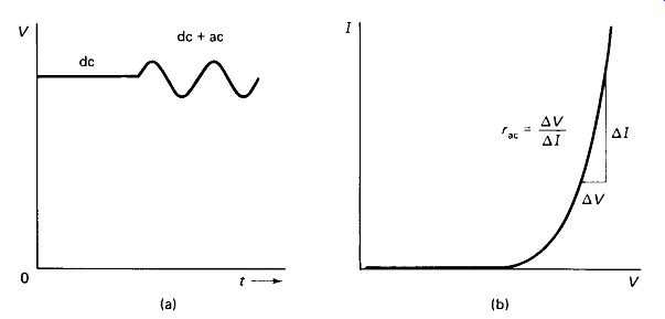
FIGURE 8-13 (a) Ac signal superimposed on a dc level, (b) The resistance
a diode presents to the ac component equals the slope AV/AI, which varies
drastically with the dc level on which the ac rides.
This ideal is not reached in actual transistors, whose dynamic emitter-junction resistance is more accurately given with values from 0.03 to 0.05 V substituted for Shockley's value in equation 8-6. /y, of course, is the dc emitter bias current. To help develop a feeling for this relationship it may be well to contemplate that, to a small ac signal, the base-emitter junction of a transistor presents a resistance of about 40 ohm when the dc emitter current is l mA, dropping to 4 B if IE is raised to 10 mA. The base supplies only l //? of the total junction current, so the ac resistance presented from base to emitter is /8/y. For a transistor with /3 = 100 this means a base input resistance to ac of 4000 ohm for IE = 1 mA, dropping to 400 B at IE = 10 mA.
A stab at this concept may appear on the data sheet as the somewhat futile hib specification, which is hardly a function of the transistor at all, but rather of its emitter current. hib is the junction resistance which we have termed rJy and hie is the base input resistance irj.
Remember that these "resistances" appear as such to small ac signals only. To dc and large ac signals, the base-emitter is a diode, dropping a fairly constant fraction of a volt.
8.8 OUTPUT RESISTANCE AND OBSCURE PROPERTIES
The ideal transistor has a collector current which does not depend upon collector voltage, but in practice Ic always increases a little with VCE-more so in germanium than in silicon, and more at high currents than low currents. This voltage/current ratio represents a dynamic resistance from collector to emitter, which appears in parallel with the regular load resistance, and may be a real limiting factor in very high gain circuits. Data sheets specify the reciprocal of collector resistance as hob for the common-base circuit or hoe for the common emitter. The relationships between them are t hoe hfehob The parameters vary widely for different collector voltages and currents, and can be compared only at identical operating points. Figure 8-14 illustrates r .
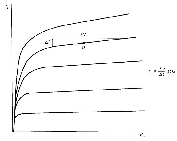
FIGURE 8-14 Transistor collector dynamic resistance generally decreases
at higher lc and lower VCE Reverse-Voltage Transfer: Ideally, a transistor
is a one-way device-input signals are fed to the output, but signals at the
output are not fed back to the input. In fact, however, a change in collector
voltage does reflect a slight in-phase change back to the input in the common-emitter
and common-base modes. Typically, the reflected input voltage is on the order
of 1/1000 to 1/10,000 of the output voltage, making the fed-back voltage
negligible in almost all cases. The ratios are given by the parameters hre
and hrb, respectively, in common-emitter and common-base configurations.
Odd-Quadrant Operation: Silicon NPN planar transistors are, of course, normally operated with positive voltages on both collector and base, but they will function with reduced performance when negative collector voltages are applied, as shown in Fig. 8-15. Beta is reduced from about 80 to 8, and the negative collector breakdown voltage is below 10 V, less than one-fifth of its forward value. The base voltage must still be positive. Negative base voltages simply turn the transistor off for both collector polarities.
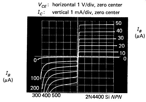
FIGURE 8-15 Quadrant 3 operation of an NPN transistor: positive lB but negative
VCE and lc. Notice the lB scale change.
SWITCHING-TIME LIMITATIONS
Transistors are often employed as high-speed switches, and the speed with which they respond to an input switching pulse is therefore of considerable importance.
Switching-time limits are divided into four parts, as illustrated in Fig. 8-16. Rise time always refers to the increasing currents at turn-on, fall time to decreasing currents at turn-off, regardless of the slope of the voltage waveform involved. Rise and fall times are defined as the transition periods between 10% and 90% of full current. Hopefully, the rise and fall times of the input pulse will be much shorter than those of the transistor under test, but if not, it will be necessary to pick beginning and end points on the input pulse for reference.
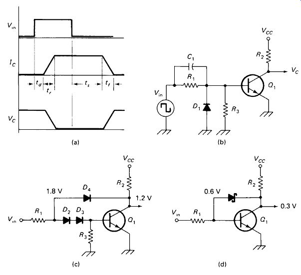
FIGURE 8-16 (a) Transistor switching-time definitions, (b) Capacitor C,
and resistor R3 drain charge carriers from the base, reducing storage time,
(c) Three-diode clamp to eliminate base saturation and stored charge, (d)
Schottky-diode clamp.
Delay Time, td, is the time from the start of the input pulse until the collector current reaches 10% of its final value. To start the turn-on process, the base-emitter voltage must be raised from its turn-off level to approximately 0.6 V. This requires that the input current first charge the emitter-base capacitance, and any associated stray wiring capacitance, to this level. Shorter delay times can therefore be achieved by:
1. Choosing transistors and circuit arrangements for low base capacitances
2. Using low-resistance drive circuits (low R1 )
3. Shunting diving resistors with capacitors to increase initial charging of base (C,)
4. Limiting the level of the off voltage to about 0.4 V, or at least preventing it from going negative (/>,) Rise Time: When the transistor begins to turn on, the collector voltage will drop, and the collector-base capacitance will couple this drop back to the base, limiting its voltage rise. This capacitance must be discharged from Vc(olf) to VC(on) by the base input current before turn-on can be completed. Rise time can be shortened by:
1. Selecting transistors and circuit layouts for low collector-base capacitance
2. Using low-resistance dive circuits (-Rj) and speedup capacitors (C,)
Storage Time: In a simple transistor switching circuit, storage time ts is usually much greater than the other components of switching time. Fortunately, storage time can be dramatically reduced by fairly simple circuit improvements. Storage time is a delay between the end of the base pulse and the beginning of collector turn-off. It is due to the fact that the base region of the transistor stores the extra charge carriers injected by base currents above the saturation requirement (IB = Ic/Beta). These carriers must be diffused or drained away before the transistor can even begin to turn off. One way to minimize storage time is to provide a low-impedance path to ground, or better yet to a negative source, to drain off the stored charge. This can be accomplished by:
1. Keeping dive resistor R1 (Fig. 8-16), and the off-state impedance of the source low.
2. Shunting the drive resistor with a speed-up capacitor, C,.
3. Providing a resistance R3 from the base to ground or to a negative supply.
4. Using a source pulse which swings negative, rather than simply zero in the off state. The resulting base discharge current is often termed /B2, as opposed to the base turn-on current I_B1. I_B2 can be calculated as (V_in(off) + V_BE)/ R_1.
Saturation Clamping: An even more effective method for reducing storage time is to eliminate the stored charge carriers by preventing the base current from exceeding the saturation requirements in the first place. This cannot be done reliably by choosing Vin and to produce exactly the required current I_C/Beta, because Beta varies so drastically from unit to unit and with temperature. Base current available must always be somewhat more than the maximum anticipated requirement, making it far in excess of the average requirement.
Figure 8-16(c) shows a three-diode saturation clamp which diverts all extra drive current through D4. Assuming that each diode junction drops 0.6 V, DA begins to conduct when VCE equals 1.2 V, routing all further drive current through the collector. Turn-off can therefore begin immediately upon removal of drive current. The minimum Vce is, of course, 1.2 V-considerably higher than in an undamped circuit. Eliminating D3 will reduce this to 0.6 V, but this should be attempted only in low-current applications where V_CE(sat) of the transistor is 0.3 V or less. In low-current applications where V_CE-(sat) of the transistor is 0.2 V or less, a Schottky diode can be used to clamp the collector at about 0.3 V, as shown in Fig. 8-16(d). This clamp is the basis for the 74S00 series of high-speed TTL integrated circuits.
Fall Time: t_f is controlled by the same factors as rise time and responds to the same treatments given previously.
Specifying Switching Times: Transistor manufacturers often combine td and tr into a single specification t_on. Less commonly, t_s and t_f may be combined as t_off.
In any case, the values given are valid only for the given test circuit, which must be specified down to the stray capacitances and inductances of the test fixture.
Manufacturers seldom use a single standard test circuit even within the same company, let alone between companies, so switching-time specifications are generally worthless for comparison purposes. Anyone seriously interested in switching times is forced to build a test fixture representative of his application, obtain a fast pulse generator and , scope, and start testing.
8.10 JUNCTION CAPACITANCE
Each of the leads of a transistor has a small capacitance to the other leads.
The exact value depends greatly upon the bias voltages across the junctions, being perhaps 3 to 10 times greater at zero bias than at high reverse bias voltages. Again, manufacturers have established no standard bias voltages to facilitate comparisons, but seem to specify test voltages according to the phase of the moon. Two parameters are of predominant importance.
Input Capacitance: This is measured between the base and emitter at the reverse bias voltage specified. The test circuit is common base or common emitter, and the collector is an ac short or open circuit, depending upon the subscript letters of the symbol: Cibs, Cibo, Cies, or Cieo. The most commonly given of these, Cibo or simply Cib, is essentially the base-emitter junction capacitance. This is generally low enough to have a negligible reactance compared with the shunting resistance of the base-emitter junction.
Output Capacitance: This is measured between the collector and ground at the specified collector-base voltage. The test circuit is common base or common emitter and the base is an ac short or open to ground, depending upon the symbol:
Cobs< Cobo> Coes> or Coeo.
These parameters essentially represent the collector-base junction capacitance, which may determine the upper-frequency limit of an amplifier. Figure 8-17(a) shows how Coe effectively shunts the load resistor (since the base voltage is near signal ground) and lowers the amplifier’s gain at high frequencies.
Miller Effect: The collector-base junction capacitance is especially troublesome in high-frequency common-emitter amplifiers because its value is effectively multi plied by (Av + 1), as shown in Fig. 8-17(b). In the illustration Av is 10, so the output signal is inverted from and 10 times larger than the input signal. The total voltage across Coe is thus (Av + 1) or 11 times Vm, and the current through it is 11 times what would be expected if Coe were connected from the input to ground.
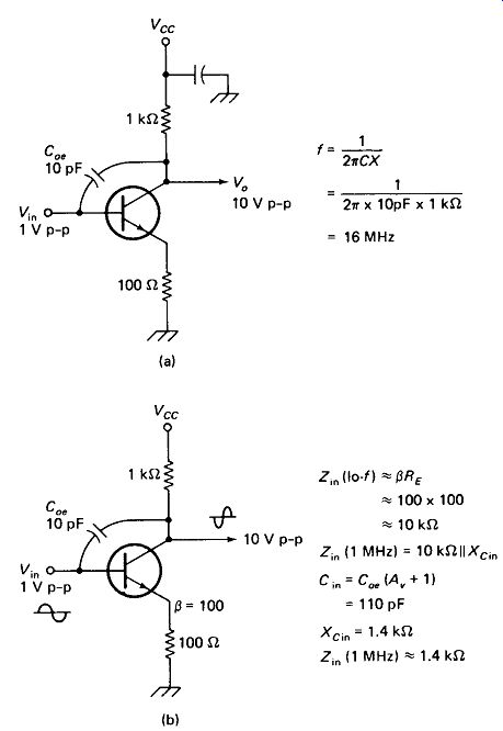
FIGURE 8-17 (a) Collector output capacitance loads the output when XCo.
- Rc. (b) The Miller effect makes C0, look (Av + 1) times larger than it
is, lowering amplifier Z_in.
Another way of expressing this is to say that the effective C_in of the amplifier is Cor ( A v + 1), which in this example is 110 pF. At low frequencies this capacitance has a negligibly high reactance, but at higher frequencies it lowers the amplifier’s input impedance, making it difficult to drive.
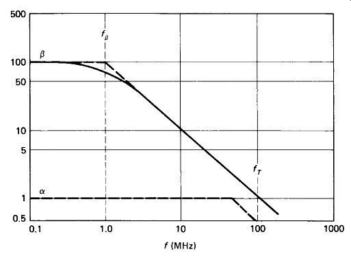
FIGURE 8-18 A transistor's gain begins to drop at fi, which equals f T//J,
and reaches unity at fT.
8.11 TRANSISTOR FREQUENCY LIMITS
At high frequencies the current gain of a transistor begins to drop off in a very predictable way, as illustrated by the curve of Fig. 8-18. There are only two variables that distinguish one transistor , s curve from another's: low-frequency current gain fi and unity-gain frequency fT. The slope of the curve in the roll-off region is always - 20 dB/decade, which is to say that the gain drops by a factor of 10 for every increase in frequency by a factor of 10. The product of current gain and frequency is constant and equal to fT in the roll-off region, so fT is termed " gain-bandwidth product."
If fT is known, current gain hfe at any frequency / can be calculated using this relationship: provided that hfe can never exceed the low-frequency current gain (i.
The frequency at which hfe begins to drop (the - 3-dB point) is termed or f_hfe, and can be calculated as The upper-frequency limit of a transistor in a common-emitter circuit lies somewhere between fp and fT and depends primarily upon the gain of the stage and the impedance of the driving source. As hfe drops off, the effect is not an actual decrease in Av but a decrease in Zin of the amplifier. As long as Zin can be maintained larger than the driving impedance Zs, overall gain will not suffer. This can be achieved by using an emitter follower to provide a " stiff" driving source or by leaving a large unbypassed emitter resistance to keep Zin high.
Common-Base Frequency Limits: The gain of a common-base amplifier depends not upon R1 but upon a, which is defined as:
(8-10)
Alpha (a) is near unity at low frequencies and is not reduced to 0.707 ( - 3 dB) until /? drops to about 2.4. The alpha cutoff frequency (/„ or f _hfb) for common-base amplifiers can be expected to be on the order of fT/2A. This is generally quite a bit higher than the cutoff for common-emitter amplifiers and accounts in part for the popularity of the common-base circuit at high frequencies.
8.12 FIELD-EFFECT-TRANSISTOR ACTION
Junction FETs: Field-effect transistors use an input voltage to control an output current. There is practically no input current except that due to stray capacitive reactance at high frequencies. The operation of an FET is quite easy to understand.
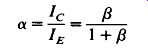
A channel of TV-doped silicon is left beneath a P-doped covering bar called the gate, as shown in Fig. 8-19(a). Normally, the channel has a resistance of a few hundred ohms, until a saturation current is reached, beyond which voltage increases produce little increase in channel current. However, if a negative voltage is applied to the gate, the P-N junction is reverse-biased, and the area around the junction becomes depleted of charge carriers as described in Section 7.1. The N channel thus becomes partially constricted; its resistance increases and its saturation current decreases. Further reverse bias causes further current restriction until the channel is finally "pinched off " entirely. Figure 8-19(b) shows a typical set of FET characteristic curves representing this process.
Notice that the elementary FET is symmetrical-the choice of source and drain is arbitrary and reversible. More important, notice that the input element is a reverse-biased diode, so the only input current is that due to leakage-typically 1 uA at room temperature and 1 uA at 150°C.
Like most semiconductors, the junction FET is available in complementary forms, in this case TV-channel and /1-channel. The P-channel devices operate with negative drain voltages and positive gate voltages with respect to the source.
MOSFETs: If a very thin layer of silicon dioxide, which is a nearly perfect insulator, is placed between the gate electrode and the channel of an FET, the leakage current is reduced by a factor of 100 to 1000, and in addition, it becomes possible to forward-bias the gate without causing gate current. When for ward-biased, the gate increases or enhances current from source to drain. This is in contrast to the depletion effect of reverse bias. These insulated-gate FETs may be termed IGFETs, or MOSTs (metal-oxide silicon transistor), but the most common verbal appellation is MOSFET (say moss-fet).
MOSFETs are available in two types.
Depletion-enhancement or Type B MOSFETs are normally partially conductive and can made to conduct more or less
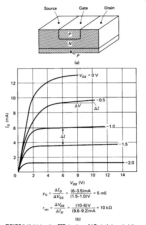
FIGURE 8-19 (a) Junction-FET structure ; (b) Typical characteristic current
by forward or reverse gate bias, respectively. Enhancement-mode or Type C
MOSFETs are normally nonconductive from source to drain and must be rendered
conductive by forward gate bias.
The Type A or depletion-mode-only FET is not designed for forward gate bias and is represented primarily by the junction FET. Figure 8-20 shows the schematic symbols for various types of FETs.
The substrate lead of the MOSFETs is generally connected to the source. The dual-gate FETs are especially suited for use as signal mixers.
FIGURE 8-20 Various types of FET.
FET versus Bipolar: Both the FET and the bipolar transistor have their advantages, and the choice between them will depend upon the characteristics required. On the plus side for the FET:
1. It has a much higher input resistance (> 100 M ohm compared to < 100 k ohm in typical circuits). Thus it is the first choice for voltmeter and oscilloscope input stages. This advantage disappears above a few MHz, where stray capacitance takes over.
2. It generates fewer and quite predictable distortion products when subjected to large input-signal swings. This has made it popular in radio-receiver RF amplifiers and mixers.
3. It is much less sensitive to radiation, making it highly desirable in military and space applications.
4. It is easier to produce in integrated-circuit form-requires fewer production steps and generally takes less chip area.
5. At low voltage levels the drain-source channel is essentially a linear resistor whose value varies with gate bias. No input (gate) current is injected into the output current path. This makes the FET more suitable for signal-chopping and control applications.
In favor of the bipolar transistor:
1. Bipolars are still less expensive and more readily available in a wide range of power levels, voltage levels, and package styles.
2. Bipolars can operate easily from a single supply of 1.5 V or less. FET amplifiers can be made to work on 5-V supplies, but they are much more comfortable with 10 or 20 V.
3. Bipolars can turn on "harder." Output saturation voltages of a few tenths of a volt versus a few volts for FETs are typical at 10- to 100-mA output currents.
4. Bias points are easier to stabilize with bipolars. Vbe is not likely to lie outside the range 0.5 to 0.9 V for any but brute-power transistors. By contrast, a typical low-power JFET lists Vas for ID of 0.4 mA as -1.0 V min, -7.5 V max. This means that we must tolerate poor bias stability, operate with high supply voltages, use current-source or dc-feedback circuitry to stabilize bias, or resort to selecting FETs for the desired VGS.
5. Voltage gains of 100 or more per stage are easily realized with resistive-coupled bipolar amplifiers. A similar FET stage would yield a gain of perhaps 10.
6. An FET's drain current is a function of the square of gate voltage. This means that gain is higher at higher bias currents [note the unequal spacing of the lines in Fig. 8-19(b)]. The result is distortion of large-swinging signals.
7. Some MOSFETs can be destroyed by a touch of the finger due to static electric charges. The caution required around these devices is explained in the next section. Many MOSFETs are protected against this hazard by integrated avalanche diodes.
8.13 FET PARAMETERS
Maximum Power and Voltage: FET ratings of maximum internal temperature T_opr, thermal resistance to case Theta j- c, and device dissipation P_T are similar to those for bipolar devices.
Avalanche breakdown is guaranteed not to occur below BV_DS for drain to source. Figure 8-21(a) shows avalanche breakdown, which is nondestructive if drain current is limited by external resistance.
For a junction FET the maximum forward gate-source voltage is that of a conducting silicon diode-about 0.6 V. The reverse limit, V_GSS, is the avalanche voltage of the gate-channel junction and is typically between -25 and -75 V.
Care must be taken that this limit is not exceeded, or that a very high impedance appears between the gate and any possible higher-voltage source, as a few milli amperes at this voltage could destroy the gate.
FIGURE 8-21 (a) FET characteristic curves showing breakdown voltage B V_DS. (b) At low reverse drain voltages, r_DS is controllable by V_S.
MOSFETs have a somewhat different gate-voltage limit. The gate-insulating layer is of necessity extremely thin, and can be arced by voltage on the order of 100 V or less. Static voltages far beyond this are commonly present on ungrounded metal objects, clothing, plastic table and chair surfaces, and so on. The destructive mechanism here is an actual capacitive-dielectric arc, not a semiconductor avalanche, and the damage is generally irreversible. Some MOSFETs have a pair of back-to-back zener diodes integrated from the gate to the source, but this protective measure adds stray capacitance, and the leakage current of the zeners reduces the input resistance of the insulated gate (although it is still many orders of magnitude higher than bipolar input resistances). Unprotected MOS devices are shipped with protective clips or pads shorting the leads to prevent destruction of the gates by static charges during handling. These should be left in place until the device is in the circuit ready for operation. Servicing of instruments containing such devices should be done on grounded metal benches with grounded soldering pencils. Operators should wear a discharging strap to ensure that their bodies do not acquire a static charge. For safety to the operator there should be a 1-M-ohm resistor between the strap and earth ground.
DC Parameters: Leakage current from the gate to the source with the drain grounded is termed IGSS. A maximum specification is made at a stated temperature and gate-source voltage.
VGS(off) also termed pinchoff voltage Vp, denotes the voltage that must be applied from gate to source to effectively " pinch off " the channel. The point of zero drain current is rather indefinite, so an effective off current of 10 or 100 uA is commonly used. This parameter often varies drastically from unit to unit, so a maximum guaranteed value is always specified, with typical and minimum values sometimes included. Yds is specified well above the saturation region for this test.
IDSS is the drain current with the gate shorted to the source. Vds is specified well above saturation. A maximum value for this zero-bias drain current is always given, with typical and minimum values sometimes included.
Drain current 1D and gate bias Vgs are related as follows:
(8-11)
Note that drain current is a function of the square of gate voltage, as indicated by the progressively closer spacing of the curves in Fig. 8-21(a).
Enhancement-mode MOSFETs use a turn-on threshold-voltage specification in lieu of VGS(off) and IDSS. This is VTH, the forward gate-source voltage which produces a specified threshold drain current (usually 10 or 100 uA) at a given VDS.
Gain Specifications: The drain-current change caused by a given small gate-voltage change (VDS being held constant) is a measure of the gain of an FET and is termed mutual conductance gm, forward transconductance gfs, or forward trans-admittance y_fs. This specification is always made with a high V_ds as its value decreases severely in the saturation region. The value of y_fs also depends on bias point, being largest at high drain currents and approaching zero at pinchoff.
In particular:
(8-12)
Figure 8-19(b) shows how yfs can be measured from a characteristic-curve display.
This parameter is also liable to vary considerably from unit to unit, and minimum guaranteed values are generally given on the data sheet.
Output Resistance: The drain of an FET presents a resistance to any ac signal appearing there because a drain-voltage change causes a drain-current change, VGS being held constant. This is illustrated in Fig. 8-19(b). This dynamic output resistance, called r0„, appears in parallel with whatever external load is connected to the drain. If the load resistance is very high, rOSJ may become the limiting factor in amplifier gain.
The output resistance decreases drastically as Vds approaches the saturation region. At VDS = 0 the parameter is called r_ds(on).
Stray Capacitance: A capacitance of typically a few pF appears from the gate to source (Cg]) and from the gate to drain (Cgd) of an FET. Manufacturer*s data sheets often specify total input capacitance C,„, which is the sum of Cgd + CgJ, and reverse-transfer capacitance Crss, which equals Actual input capacitance of an amplifying circuit may be many times larger than C,„ because of the Miller effect, as explained in Section 8.10.
Control Applications: As shown in Fig. 8-21(b), FETs have a drain-to-source resistance which transitions smoothly from a few hundred to many thousands of ohms if VDS is kept in the range of ± IV or so. The FET can thus be used as an electrically-operated variable resistor, with gate voltage determining resistance.
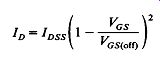
Figure 8-22(a) shows a simple automatic gain control for an audio preamp utilizing this property. The control input is dc-rectifie4 and filtered from the audio output.
The dc becomes more negative at high audio levels, thus automatically turning the gain down. In another application, the control signal could be derived from a microphone picking up crowd noise in a lobby. Less negative dc would be delivered for higher crowd noise levels, thus automatically increasing the gain of the PA amplifier.
FIGURE 8-22 (a) FET used as an electrically variable resistance to control
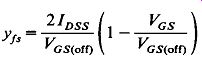
the gain of a bipolar amplifier, (b) Pair of FETs used o switch two Inputs
alternately to a single line.
Figure 8-22(b) shows a simplified dual-trace oscilloscope chopper. The gates are fed from the oppositely phased outputs of a multivibrator, turning on alternately the channel A and channel B FETs. Since the gates are never forward-biased, the chopping square wave is not passed to the output. The chopping frequency must be kept reasonably low, however, to prevent from passing the chopping signal to the 10-k-ohm resistor. The A and B input signals must not become large enough to interfere with the on-off switching signal. For JFETs, this limits the inputs to a few tenths of a volt. MOSFETs will handle much larger signals, since the switching square waves can be of both polarities (say, ± 10 V) without causing the gate to conduct. Integrated circuits containing several of these MOS bilateral analog switches are available.