9.1 THE UNIJUNCTION TRANSISTOR
Next to the diode and the bipolar transistor, the UJT is the oldest of the semiconductor devices. It is a switching device with two stable states: on and off.
The main current path is from emitter to base 1, as shown in Fig. 9-1. This path is normally an open circuit, but it switches to a near short circuit if the emitter-base-1 voltage reaches a critical percentage of the inter-base voltage Vn_BV This percentage is determined by the intrinsic standoff ratio 17 (eta), a property of the UJT which generally lies between 0.85 and 0.55:

(9-1)
... where VD is the silicon-diode drop, approximately 0.6 V.
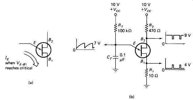
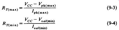
FIGURE 9-1 (a) Schematic symbol, lead identification, and main current path
for the unijunction transistor, (b) Basic UJT oscillator with representative
waveforms at the three terminals.
The similarity of the UJT symbol to the junction FET symbol is unfortunate, because the two devices have almost no similarities from an operational point of view. The UJT is not usable as an amplifier, since it triggers abruptly from off to on and has no continuous range in between as do bipolars and FETs.
UJT Oscillator: The circuit of Fig. 9-1, in one form or another, probably encompasses more than three-fourths of all UJT applications. It is an RC oscillator whose advantages include simplicity, frequency stability with temperature and supply-voltage change, and sawtooth and pulse-shaped outputs. The operation of the circuit is as follows:
1. Timing resistor RT charges CT toward cc according to the familiar iC-time-constant formula. The UJT is off, so the emitter draws no current.
2. When the emitter voltage reaches the critical level, the emitter to 2?, path becomes a very low resistance, and CT discharges through Ru producing a positive pulse across R1 . The voltage across CT drops much more quickly than it rose, because it discharges through R1 which is much smaller than R_T.
3. When the UJT turns on, the inter-base resistance drops, causing a negative going pulse at B2. For a typical UJT in the circuit shown, this may consist of a drop from 9 V to 6 V.
4. When the capacitor is nearly discharged, the emitter current drops below a minimum hold-on value, and E-B_1 returns to its normal open-circuit state, allowing another charging cycle to begin.
Outputs may be taken from any of the three UJT leads, provided that the impedance of the load is several times the value of the associated circuit resistor. This imposes a stringent requirement on the sawtooth output at the emitter because R_t is usually a high value.
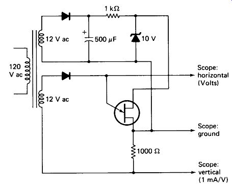
FIGURE 9-3 UJT curve tracer adapter for use with a conventional dc-coupled
oscilloscope.
It may be difficult to obtain more than a few volts at Bi because of internal-device resistance. R1 can be eliminated if the positive pulse output is not required.
The circuit will function without R2, but it has two other functions besides producing a negative-pulse output. The failure rate for semiconductors is much higher than for resistors, and without R2 an inter-base short amounts to a destructive power-supply short. R2 also provides frequency stability against temperature variations by compensating for decreases in the VE_BX diode drop at elevated temperature. The inter-base resistance rBB rises at high temperature, increasing VB2~B\i which tends to increase the firing voltage. With proper selection of R2, this effect will just offset the decrease in emitter-diode drop, keeping the firing voltage constant. R2 is determined by:
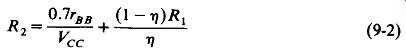
[9-2]
UJT Characteristics and Limitations: Figure 9-2(a) shows the structure of a bar-type UJT. The bar is TV-doped to have a resistance generally between 1 and 10 k-ohm. A P-doped pellet is alloyed to the side of the bar, its position determining the firing voltage-to-interbase voltage ratio rj. A schematic representation is given in Fig. 9-2(b). The ratio rB1/(rB1 + rB2) equals rj. Upon firing, rBl decreases drastically. The emitter diode has a drop of about 0.55 V at room temperature for typical UJT firing currents. Figure 9-2(c) shows a planar-UJT structure which generally has lower reverse leakage in the emitter diode than the bar type.
A complete description of a UJT's parameters is given by its characteristic curve of IE versus VE_BX, shown in Fig. 9-2(d) with the low-current range expanded for clarity. This curve can be displayed on a conventional transistor curve tracer if a separate + 10-V supply is connected from B2 to £,. The " collector " terminal feeds the UJT emitter, and the "base" step output is unused. The circuit of Fig. 9-3 can be constructed to display the curve on a standard oscilloscope. The curves will be upside down, but this should present no problem.
Following the curve from the lower left, 1E_B20 is the reverse leakage current through the emitter diode when VE is zero and Vbi is the +10 V. Its value is typically a few nano-amperes at 25 °C, remaining less than 1 /xA even at maximum operating temperature for planar UJTs. Bar-structure UJTs may have several pi A leakage, even at 25 °C. This current must be small compared to the current supplied by the external timing resistor if timing and waveshape at the emitter are to be unaffected by leakage.
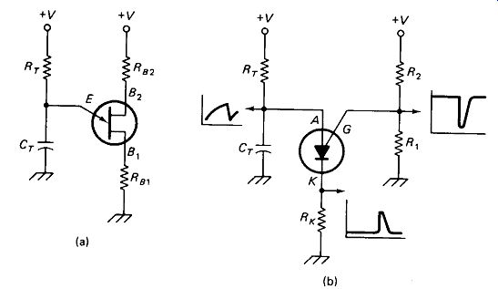
FIGURE 9-4 Comparison of the basic oscillator for the conventional UJT (a)
and PUT (b). R, and R 2 determine the firing voltage VA(crll).
As emitter voltage is increased, the emitter diode becomes forward-biased and forward current begins to flow. The current required to fire the unijunction is called the peak current and Kpk is the firing voltage. The standoff ratio can be obtained from as
Peak current is typically in the neighborhood of 10 uA for bar UJTs, down to 1 uA or less for planar types. It is essential that the timing resistor be able to supply adequate firing current (V_pk) with the emitter at the threshold of firing (Fpk). To maintain timing accuracy and waveform purity at the emitter, IRT must be many times larger than I_pk.
Upon firing, the UJT switches very rapidly to the on state, as indicated by the dashed line. This transition cannot be displayed accurately by the curve tracer, but that is not important. VE_ Bi is typically between 1 and 2 V in this region, rising slightly with rising emitter current. The critical parameter of this on region is the minimum or valley current required to maintain the device in the on state. This may be 10 mA or so for bar-type down to 1 mA for planar-type UJTs. In the oscillator circuit it is essential that the timing resistor not supply enough current to hold the UJT in the on state with VE_Bl at the valley voltage.
Using these facts, we can develop formulas for the maximum and minimum values of the timing resistor in the UJT oscillator circuit:
[9-3]
Vcc is the supply voltage.
Note that these formulas contain no safety factors. Good design practice would keep RT between half the maximum and twice the minimum calculated values.
FIGURE 9-2 (a) Bar-structure UJT. (b) UJT equivalent circuit, (c) Planar
structure UJT. (d) UJT characteristic curves.
Programmable UJTs or PUTs offer certain advantages over the bar and planar UJTs. Figure 9-4 shows the comparison. Internally, they are four-layer PNPN devices similar to the SCR (Section 9.3). Externally, they behave like a conventional UJT, with these differences:
1. There is no intrinsic t] factor. The device turns on when VA becomes greater than VG by an amount specified as offset voltage VT, a value that may lie between 0.2 and 1.6 V.
2. The firing voltage is selectable or "programmable" by adjusting the gate voltage with a voltage divider R1-R2. (Actually, the term program refers to a sequence of events, not a selection of a single event, but we seem to be stuck with this perversion of the word.) The firing-voltage variation thus depends upon resistor tolerance, not semiconductor tolerance, and can be held at 10% or 2% from unit to unit if you are willing to pay for the precision resistors (5% or 1% tolerance, respectively). This is a great improvement over the conventional UJT. The gate leakage current IGA0 is typically 10 uA at 25°C, increasing to around 100 uA at maximum temperature.
3. Valley current Iv is a function of the Thevenin equivalent of Rx || R2 (termed Ra) and, to a lesser extent, of gate voltage VG (also termed Fs).
There seems to be no formula relating Iv to Rc, but for one PUT type lv was 300 /nA at RG = 10 ki, decreasing to Iy = 18 ft A at RG = 1 Ml. Other PUTs have Iv as low as 25 /nA at RG = 10k ohm. These values are in general much lower than for conventional UJTs, dictating a much higher minimum value of RT.
4. The turn-on time is generally somewhat less for a PUT than for a UJT.
PUT oscillators are nevertheless limited to frequencies below about 50 kHz because of the low hold-on current and consequent high minimum Rt. Conventional UJTs can oscillate up to about 500 kHz.
5. The on-state voltage drop (VAK, also termed VF) is typically about half the VE-b\ a conventional UJT.
6. The gate is brought forcibly to within a few tenths of a volt of ground in the on state, producing a very respectable negative-going pulse output. By
contrast, the conventional UJT brings B2 to only a few volts above ground through an impedance of perhaps a few hundred ohms.
7. Leakage and firing currents IGAO and /pk are similar or slightly lower than those of the UJT.
Complementary Unijunction Transistors (CUJT) are available, although their popularity seems much less than that of UJTs and PUTs. Internally, they consist of a four-layer NPNP sandwich (complementary to the PNPN layers of the PUT) with integrated resistors and R2 determining the intrinsic standoff ratio tj. CUJTs can be applied in the standard circuit on a negative supply, or inverted on a positive supply, as shown in Fig. 9-5.
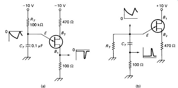
FIGURE 9-5 Oscillator circuits for the complementary UJT: (a) with negative
supply; (b) positive supply.
FIGURE 9-6
UJT Circuit Applications: UJTs are used as oscillators and sweep generators with frequencies from one cycle every few minutes up to a few hundred kHz, as timers over the same range, as voltage-sensitive triggers, as pulse generators (especially for triggering power devices such as SCRs), and as simple frequency dividers (by relatively small integers, such as 7 kHz to 1 kHz). Figure 9-6 shows a number of these applications.
9.2 THE 555 TIMER
Since its introduction in 1972, the NE 555 timer IC has achieved such widespread industry acceptance that we feel justified in treating it as a standard component.
Although called a timer by most manufacturers, the 555 is a general-purpose device with additional applications as an oscillator, free-running or triggered pulse genera tor, ramp generator, frequency divider, and frequency, pulse-width, or pulse position-modulated oscillator, to name a few.
--------- 213
Outputs: The pin connections for the 555 timer and pin function names are shown in Fig. 9-7. The device operates on a positive supply between 4.5 and 16 V.
It has a low-impedance (totem-pole) pulse output which switches between Vcc and ground, less 0.1 V or so for transistor saturation.
A second discharge output is connected to an open-collector transistor which pulls low when the output goes low. This is generally used to discharge the timing capacitor at the end of a cycle.
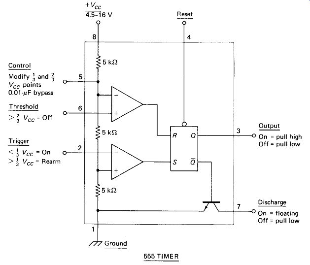
FIGURE 9-7 Pin connections and representation of internal functions of the
popular 555 timer IC. Inputs are on the left, outputs on the right.
Inputs: There are two primary inputs, one to begin and one to end the cycle. The trigger input initiates a high output when its input is driven below 1/3 Vcc. The output then remains high, regardless of any further changes in trigger voltage. Notice that the trigger input voltage must be returned to a level above 1/3 Vcc to re-arm the trigger function. Successive triggering cannot be accomplished by simply holding the trigger input low.
The second input (threshold) resets the output to low and turns on the discharge transistor when its voltage level goes above f Vcc. This input is most often connected to the timing capacitor to reset the device when the capacitor voltage rises to 2/3 Vcc.
Reset and Control Functions are not used in elementary timer applications, but these input pins must be properly connected in any case. A low voltage (below 0.4 V) at reset directly turns on the discharge transistor, ending the cycle prematurely and bringing the output low. Normally, reset is connected directly to the Vcc pin hi level.
The voltage at the control input is normally held at 2/3 Vcc by the three internal 5-k-ohm voltage-dividing resistors.
Varying this voltage by either dc or ac coupling alters the trigger-on and threshold-o/jf voltages. A more positive control lengthens the on time, and increases the trigger level. Voltage control of oscillator frequency, pulse duration, and pulse position are possible via this input. Normally, control is bypassed to ground with 0.01 uF to prevent noise pickup.
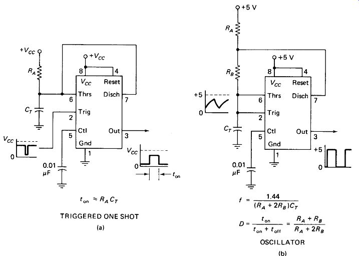
FIGURE 9-8 The two basic 555 circuits upon which most others are developed:
(a) one-shot; (b) oscillator.
Applications: Figure 9-8 shows the two basic 555 circuits upon which most others are based. The triggered one-shot of Fig. 9-8(a) is the basis of most time-delay, pulse-stretching, frequency-dividing, and sweep-generating applications. An input pulse less than 1/3 Vcc at pin 2 initiates the output. Pin 2 may be held at 1/2 Vcc with two 100-k Ohm resistors between V_cc and ground, and the pulse coupled in via a capacitor to increase sensitivity. When RA charges CT to 2/3 Vcc, threshold pin 6 turns pin 7 on to ground, and the output goes to zero until the next trigger pulse. A positive voltage at the control input will lengthen the output pulse. An ac signal several times lower in frequency than the trigger rate will produce pulse-width modulation. If the time between trigger pulses is less than t_on, the circuit will lock to a sub-multiple of the trigger rate, serving as a frequency divider.
Figure 9-8(b) is a free-running oscillator. The circuit triggers itself because the trigger input is connected to the timing capacitor. The voltage across CT oscillates between | C (the trigger-on level) and 2/3 C (the threshold-off level). The discharge of CT can be made almost instantaneous by reducing RB to zero. Frequency modulation can be achieved by coupling a low-frequency signal to the control input through a capacitor. A voltage-controlled oscillator is produced if a dc level is connected directly to pin 5.
Specifications: The following table summarizes the chief characteristics for the 555 IC timer:
9.3 SILICON-CONTROLLED RECTIFIERS
In the section on transistors we made quite a point of the fact that the power burned in any device is zero if the voltage across it is zero, regardless of the current it may carry. Likewise, the power is zero if the current is zero, regardless of applied voltage. A device that switches instantly from a perfect short circuit to a perfect open circuit can thus be used to control large amounts of power without burning any power itself. The mechanical SPST switch is the perfect example of this, but it is terribly slow and suffers from wear of the moving parts.
An SCR is like a very fast electronically actuated switch in series with a diode.
This switch is turned on by applying a brief current to the gate lead, as shown in Fig. 9-9. Turn-off cannot be accomplished by gate control; rather it results from interrupting the forward current through the device.
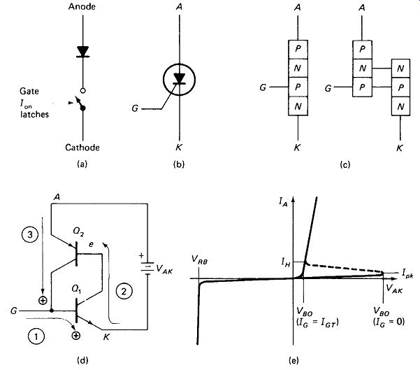
FIGURE 9-9 (a) Representation of the SCR function, (b) SCR symbol and lead
identification, (c) Internal SCR structure and similarity to coupled PNP-NPN
transistors, (d) Two-transistor equivalent of the SCR showing self-latching
current paths, (e) SCR V versus I characteristic curve.
Two-Transistor Equivalent: Internally, an SCR consists of a four-layer sandwich of PNPN-doped silicon [Fig. 9-9(c)]. This is equivalent to two complementary transistors interconnected as in Fig. 9-9(d). Notice that once a gate turns Qx on, the Qx collector supplies turn-on current for the base of Q2. Once turned on, Q2 supplies turn-on current for the Q, base, holding it on regardless of any current from the gate. Reducing or even reversing the gate current will not turn an SCR off once it has fired.
SCR Applications most commonly make use of phase control of an ac line. This is illustrated in Fig. 9-10. If the SCR is fired early in the ac positive half-cycle, the average load power is one-half of that obtained by connecting the load directly to the line. However, if the SCR is gated on later in the half-cycle, the load power is reduced-to one-fourth at 90°, and eventually to zero as the " firing angle" approaches the end of the positive half-cycle at 180°.
Most of the fun of designing SCR circuits lies in finding more clever ways to trigger the gate at the desired point of the cycle. The objectives of the game are:
1. Trigger with a fast-rise pulse rather than with a ramp or sine wave. The gate firing current varies widely among units and with temperature, making pulse triggering the only stable way.
2. Make the pulses strong and brief. High gate currents make faster turn-ons, and hence less power is dissipated in the device. The average gate power limit must not be exceeded, however, so large gate currents must come and go quickly. Negative gate voltages waste gate power and are a definite no-no.
3. Cover the entire range of firing angles from 0° to 180°, but do not waste too much of the control range on the 0 to 30° delay angles, since there is little power difference between them.
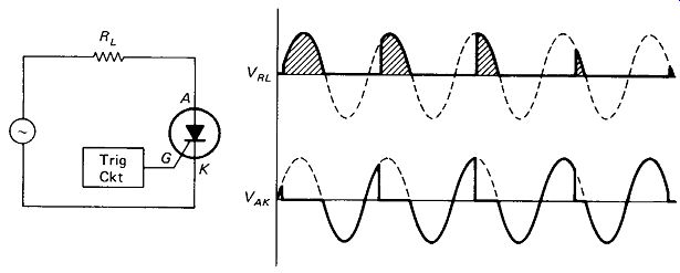
FIGURE 9-10 Decreasing average load power as SCR firing-delay angle progresses
from 0 to 180°. Real-life progression generally takes hundreds of cycles.
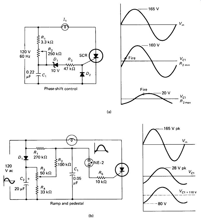
FIGURE 9-11 (a) Simple but rather unreliable method of triggering an SCR
by varying the phase and amplitude of the voltage across C,. (b) More stable
and reliable SCR trigger circuit with constant phase shift across C, but
a variable dc voltage tapped from C2 by R3.
Figure 9-11 (a) shows a phase-shift firing circuit which violates most of the foregoing rules. Triggering is not done with pulses, but with a sine wave phase-shifted so that it rises sufficiently positive to trigger the gate at the desired point. R1 R2, and C are chosen to provide a capacitor phase lag adjustable from about 15° to 75°.
With R2 at its minimum, the voltage rises quickly and the SCR triggers before 20°, giving nearly 50% of full-wave ac power to the load. With R2 at its maximum, the voltage is delayed by 75° and rises more slowly, so triggering may be delayed to ...
FIGURE 9-11 (c) Highly stable SCR trigger using a UJT and variable charge
time on C.
... about 160°, giving less than 5% of full output. The circuit requires a sensitive-gate SCR (0.5 mA or less trigger current) and is quite sensitive to temperature and unit-to-unit variations. The diode on the gate prevents negative gate current and equalizes the load in the positive and negative directions.
Figure 9-11(b) shows an improved SCR lamp control using a neon lamp to generate a fast-rise gate-trigger pulse. R1 R2, and the 120-V line have a Thevenin equivalent of approximately 60 V through 75 k ohm, feeding a 70° lagging sine wave of 28 V pk to C,. This wave is on the rise (-28 to +28 V) during most of the positive half-cycle of the line. The NE2 lamp fires at about 80 V, dropping immediately to 60 V, and the 20-V difference generates a 2-mA pulse through the 10-k ohm resistor.
The 80-V level is achieved by adding a variable dc level to the 28-V-pk sine wave across C,. /),, C2, R3, and R4 comprise a +64- to + 160-V dc supply, which, through division with R2 and R1 , supplies a maximum of +80 V dc to C,. Varying the amount of dc imposed varies the point at which the sine wave will bring the total voltage to the critical 80-V level.
Figure 9-11(c) shows a different approach to triggering an SCR which allows the load to be placed directly in series with the entire SCR circuit. This is quite an advantage, since it means that an existing remotely located light switch can be replaced with the "dimmer" control. Assuming an 8-k Ohm rBB for Qt, Dx and R1 bring the top of D2 up to + 10 after the first 10° of the positive line cycle. Zener action holds this point at + 10 V for the remaining 170° of positive line.
R 2 and R 3 charge C to the UJT firing voltage (about 7 V) after a time that can be varied from 0.2 to 10 ms. This spans essentially the entire positive half-cycle (0 to 8.3 ms for a 60-Hz line). When the UJT fires, a short fast-rise pulse (duration «/?4C or about 2 jus) triggers the SCR gate. At the end of the positive half-cycle the UJT B2 voltage falls to zero, causing the emitter to fire and discharge the capacitor in preparation for the next cycle.
This circuit is not sensitive to variations in gate trigger current, and trigger pulses are bief, keeping average gate power low. The RC network is isolated from the SCR gate by the UJT, so that there is no hysteresis effect. A power diode D3 is shown switchable across the SCR to allow the negative half-cycle through the load, providing Variable control from 50% to 100% of full power. This same technique can be applied to the previous two circuits.
Figure 9-12 gives several additional SCR applications. The first is a full-wave version of the UJT-triggered lamp dimmer. A diode bridge converts the ac line to all-positive pulses before application to the SCR and control circuit. This technique is not generally applicable to phase-shift triggering circuits such as those in Fig. 9-11(a) and (b). The load current is ac with the circuit wired as shown, but dc load current can be achieved by placing the load in series with the SCR anode.
Figure 9-12(b) is an automobile battery charger with automatic shutoff. When the battery voltage charges up to about 13.5 V, the gate-to-cathode voltage becomes too low (0.5 V) to trigger the SCR.
Figure 9-12(c) is a speed control for universal (series field and armature) motors, such as are common in hand dills, sewing machines, and food mixers (but not in household fans, record players, and bench tools). The circuit balances the induced voltage produced by the motor against the wiper voltage from R2. As the motor slows down due to increased load, induced voltage is reduced, and the SCR fires earlier in the positive half-cycle. Raising the wiper voltage raises the required induced voltage and hence motor speed.
Figure 9-12(d) provides a 30-second time delay before turning on the SCR, which is used as a rectifier in a high-voltage supply. Such a circuit is useful in systems containing a CRT or other heated-filament device, to allow warmup time before applying high voltage. The UJT fires the low-power SCR, after a delay time set by R1 C,. SCR, then remains on as long as the +5-V supply remains on. This turns on the LED, which is optically coupled to the photoresistive cell, lowering its resistance and allowing the high-power SCR2 to fire on each positive half-cycle. Note that the photocell must be able to withstand the peak secondary voltage until C2 becomes charged.

FIGURE 9-12 Six SCR applications. Transformerless low-voltage supply ; Crowbar
overvoltage protection.
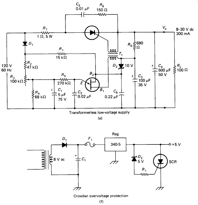
FIGURE 9-12 (Continued).
Figure 9-12(e) is a low-voltage dc supply operating directly from the ac line without transformers or power-wasting series-dropping resistors. Since one side of the line is connected directly to the negative output of this circuit, adequate precautions should be taken to ensure that contact between the circuit and earth ground cannot occur. On the positive half-cycle, £>,,/{,, and D2 bring the B2 reference of the UJT rapidly to + 10 V above VQ, which is initially zero. R2, R3, and RA form a variable voltage divider charging C, to a positive value between 20 and 50 V. The time constant for charging C, is about 0.25 s. This slow rise is important because it raises the output voltage demand slowly, preventing destructive voltage and current surges at turn-on. Rs charges C2 toward reaching the firing point of the UJT just as the positive half-cycle of the line is nearing its end. The discharge of C2 through pulse transformer T, fires the SCR, charging C4 after several cycles, to (let us say) + 20 V. R6 and C3 filter the ripple from VQ and D2 now clamps the B2 voltage at VQ + 10, or 30 V. VBB is still 10 V, since Bx is referenced to VQ.
If VQ rises (due perhaps to loss of load) R5 takes longer to fire the UJT because of the lesser slope of the charge curve at higher voltages and the fact that the R5 source voltage is referenced to ground, not VQ. This later firing means that the line voltage drops nearer to zero before it charges C4, tending to bring V0 back down. Load regulation of 10% for a 200-mA load at V0 = 20 V is achieved by this feedback. Line regulation could be added by zener regulating the voltage from C, before applying it to Rs. C6 maintains control voltage at B2 for a millisecond or so after the line drops below V0 + 10 V, allowing the UJT to be emitter-triggered even at delay angles approaching 180°. R-, limits surge current at turn-on. Conduction angles are on the order of 10 to 15° , and current pulses are about 20IQ for this circuit. C5 and Rs suppress line transients which could cause false triggering of the SCR. A trigger at the early part of the positive half-cycle would apply a 170-V peak to C4 and RL, which could be quite bad.
Figure 9-12(f) is a "crowbar" circuit, which has become quite popular in spite of its crude approach to circuit protection. If VQ rises above +5.6 V (due perhaps to failure of the 5-V IC regulator), the entire system it supplies is threatened with destruction. The SCR saves the system by shorting Vo dead to ground, blowing the fuse Fx.
SCR Ratings: There are well over a dozen commonly used specifications describing SCR performance. The following table of sub-script usage should be of some help in sorting out the parameter symbols:
------------
Subscript Meaning
Average Breakover Off state Forward Gate Hold-on Maximum peak Gate open Reverse (first subscript) Repetitive (second subscript) Surge (nonrepetitive) On state (First subscript) Trigger (second subscript)
---------------
Now we are prepared to examine the various ratings in detail.
Anode-Cathode Voltage
*Vrsom afd Vrrom arf maximum reverse peak surge voltage and peak repetitive voltage which the device can block without drawing reverse current. The gate must not have a positive voltage applied while a large negative voltage exists on the anode, as this causes reverse anode current of a magnitude on the order of IG. Thus a 20-mA gate current during the negative half-cycle of a 120-V line could cause an average additional power dissipation of over one watt:
= W(av)~0.5 X 0.02 X 0.9 X 120= 1.1 W
Note that the current flows for 0.5 cycle and that VAY = 0.9 Vms. A diode in series with the anode will stop reverse leakage if the gate must be positive during the negative half-cycle.
* Vdsom and Vdrom are maximum forward blocking voltages, nonrepetitive surge, and repetitive or continuous, respectively.
*V(bo)o forward breakover or firing voltage with the gate open. This firing voltage decreases for small forward gate currents below the gate trigger current, but little use is made of this fact because of extreme sensitivity to temperature and unit-to-unit Variations.
" Vtm is the forward on-state voltage, anode to cathode, for a specified forward current and junction temperature. It may be as low as 0.8 V for low currents, rising to around 2.0 V at /t-(AV) and 3.0 V at ITSM.
Anode Current
. Irom afd Idom arf maximum reverse and forward off-state anode leakage currents at a specified voltage and temperature.
. Itsm maximum rated forward on-state surge current for a specified short time, usually one cycle. ITSM is typically at least 10 times /r(AV)-
. I2t is a nonrepetitive surge-current rating intended for use in calculating fuse sizes for the protection of the SCR. If the product of fuse-blow current squared times blow time is less than I 2 t, the fuse will blow before the SCR.
. t(av) a°d /r(im!) are the average and rms maximum on-state currents allowable. Values from 0.5 A to over 2000 A are available.
These ratings are generally dependent upon conduction angle and line frequency, and are detailed in charts supplied by the manufacturer. They are given in lieu of total device power-dissipation limits, although power dissipation can some times be obtained from additional charts. All of this is quite a bit of trouble, so it may be assumed in most cases that the maximum average load current at the 180° conduction angle equals the maximum average anode current. Average power is then approximately /avKTm-
For circuits such as those shown in Fig. 9-12(e), where conduction angles are never longer than a small fraction of a cycle, the average-current specification will have to be derated because of junction heating on high-current peaks.
The exact derating depends upon the thermal time constant of the SCR in use, but the following schedule is typical for 1- to 50-ampere SCRs.
. Iho iS anode holding current, below which the SCR reverts to the off state. IL, which is typically about 50% greater than IHO, is the forward latching current which is necessary for the SCR to initially assume the on state.
Gate Characteristics
. Vgt is the dc gate voltage required to trigger the device. It is generally between 0.7 and 1.5 V positive with respect to the cathode.
. K?dm> sometimes called VGNT, is the maximum gate voltage guaranteed not to trigger the device, and is generally specified at a low value, around 0.25 V. Some spec sheets list Kcr(min) for this value.
. VGRM is the maximum reverse voltage guaranteed not to cause reverse current in the gate. It is typically in the vicinity of 5 V.
. I GT is the dc gate current required to trigger the device, and IGTM is the peak triggering current required for a specified pulse width.
. g(av) iS the maximum allowable average gate power (IGVG X duty cycle).
PGM is the maximum peak gate power for a specified short pulse time.
Time Considerations
-- t_g, is the gate-controlled turn-on time for a specified gate current and anode current. Values of a microsecond or two are typical. Time is measured from ise of the gate pulse to fall of the anode voltage. Tgl is sometimes split into delay time td (gate pulse to 10% anode current) and rise time t_r (10% to 90% anode current). Turn-on time can be reduced significantly by increasing gate trigger current.
-- t_w is the gate pulse width required to trigger the SCR for a specified gate pulse current. The relationship between tw and IGTM is generally shown in a manufacturer's chart.
t_q is circuit-commutated turn-off time for a specified IT (on current), VR (off voltage), and VD (forward blocking voltage). The SCR is triggered carrying anode current I_T. Then a reverse (or zero) anode voltage is suddenly applied. Finally, a forward voltage VD is applied. The test is repeated to determine the minimum time the forward reapplied voltage can be delayed to allow the SCR to turn off and gain forward-blocking capability. This time tq has a typical range of values between 5 and 100 usec, depending upon SCR type.
Critical dv/dt is the maximum allowable rate of rise in forward current at turn-on. Because the junction area near the gate is turned on before the rest of the junction area, localized hot spots can appear if the initial current at turn-on is allowed to rise too quickly.
Critical dv/dt is the maximum rate of change of forward anode voltage that the SCR can withstand without false triggering due to gate currents coupled in by the device , s own stray capacitance. Transients on the ac line are often responsible for such false triggering. The accepted solution for this problem is to use an RC "snubber" across the SCR, as shown in Fig. 9-13.
The values of R and C for a 120-V line can be obtained from the formulas:
_dv/dt R = 3 C=0.
1 (dv/dt)2 where R is in k ohm, C is in /xF, IL is in amperes, and dv/dt is in V/jus.
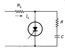
FIGURE 9-13 RC snubber to prevent false triggering of the SCR on fast-rise
line transients. Component values are given by equations 9-5 and 9-6.
SCR Power Calculations: In dealing with the chopped-up sine waves produced by SCRs, we often need to know the average and rms values of current involved in order to calculate SCR power and load power, respectively. The graph of Fig. 9-14 gives these values for conduction angles from 0 to 180° , assuming a 1-V-pk source applied to a 1-oh load, giving a 1-A-pk current at full conduction. Other peak voltage and current sources can be scaled accordingly. For do-it-yourselfers, the formulas used to obtain the chart are given:
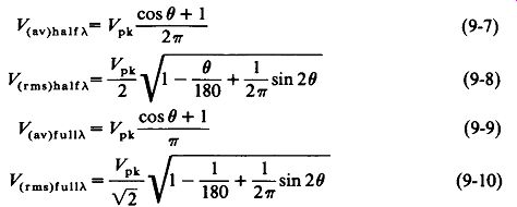
[9-7, 9-10]
… where theta is the firing-delay angle in degrees from the zero-crossing point (0°in half wave, 0° and 180° in full wave) and V_pk is the peak value of the applied line voltage.
EXAMPLE 9-1
An SCR is to supply 300 W to a 10-0 load on a 120-V-nns line by controlled half-wave rectification. Determine the firing-delay angle and the SCR power. The SCR drops 2.0 V in conduction.
Solution
The required rms current as a fraction of peak current is found:
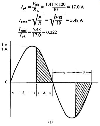
FIGURE 9-14 (a) Firing-delay angle 8 and conduction angle theta.
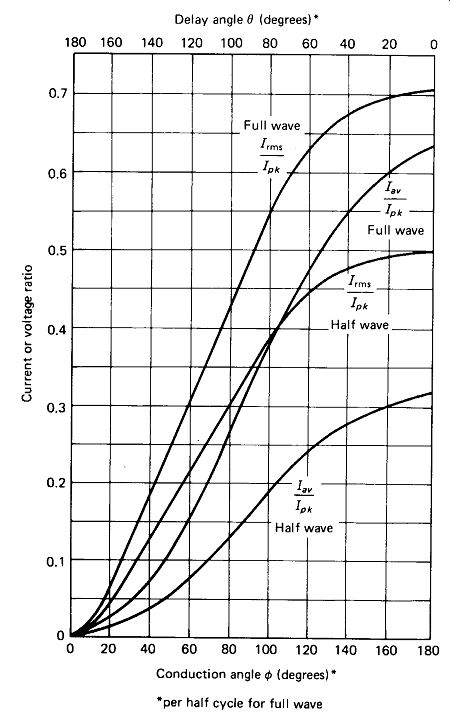
FIGURE 9-14 (b) Ratios of rms/peak and average/peak voltage or current for
SCR waveforms as a function of conduction angle.
This value appears in Fig. 9-14 at a delay angle of 97°, and the corresponding average current ratio is 0.14.
Pscr = 2.4 x 2.0 = 4.8 W
9.4 TRIACS AND OTHER THYRISTORS
The SCR was the first of the family of semiconductor devices collectively known as thyristors. None of the later additions has near the power-handling capability or the popularity of the SCR, with the exception of the triac, which is available with ratings up to 40 A and is widely used in full-wave lighting and motor controls.
Figure 9-15 summarizes the lesser-used thyristors.
Amplified-Gate SCRs: The ratio of maximum average anode current to gate triggering current is several hundred to a thousand for most SCRs, but is increased to several thousand in the amplified-gate SCR. Major operational characteristics remain unchanged.
Gate-Controlled Switch (GCS) or turn-off SCR: The anode current of this device can be turned off by a negative gate pulse while forward anode voltage is still applied. However, the negative gate current required is on the order of one-tenth the anode current, and only low-power devices are available.
Complementary SCR: The CSCR has the gate near the anode and fires with a negative pulse applied between gate and anode. It is a true complement to the SCR, operating on negative voltages as the SCR does on positive voltages.
Silicon-Controlled Switch: The SCS combines the features of the GCS and CSCR.
Both anode and cathode gate leads are accessible. It can be turned on by a positive voltage from GK to A" or by a negative voltage from GA to A. The cathode gate is extremely sensitive (/C7-k~1 ju.A), the anode gate less so (ICTA-100 /iA for a 200-mA device). The SCS can also be turned off by a negative current of approximately 0.1 IA from the cathode gate. False triggering due to high dv/dt at the anode can be completely eliminated without use of an RC snubber by the simple expedient of connecting GA to the anode supply through a 100-kl resistor and using the SCS as a conventional low power SCR. One notable application of the SCS is the latching high-voltage diver of Fig. 9-15(b). A pulse of a few microamperes at GK turns the neon lamp on, and it latches until 1A is removed.
Alternatively, IA can be pulse-width-modulated at 100 Hz or so to vary the brightness of the lamp. IGK must be continuous in this case.
Silicon Unilateral Switch: The SUS is a complementary SCR with an integrated zener diode connected from cathode to gate so that the device triggers without a gate signal when VAk exceeds the zener voltage. Commonly available SUSs are set to trigger at 8 V. The gate lead is brought out so that triggering below 8 V is possible with a negative voltage from gate to anode, although this is infrequently done. The primary application for the SUS is as a gate trigger in SCR circuits, in the way the neon lamp was used in Fig. 9-11(b). The advantages of the SUS trigger level of 8 V over the NE-2 level of 70 V are obvious.
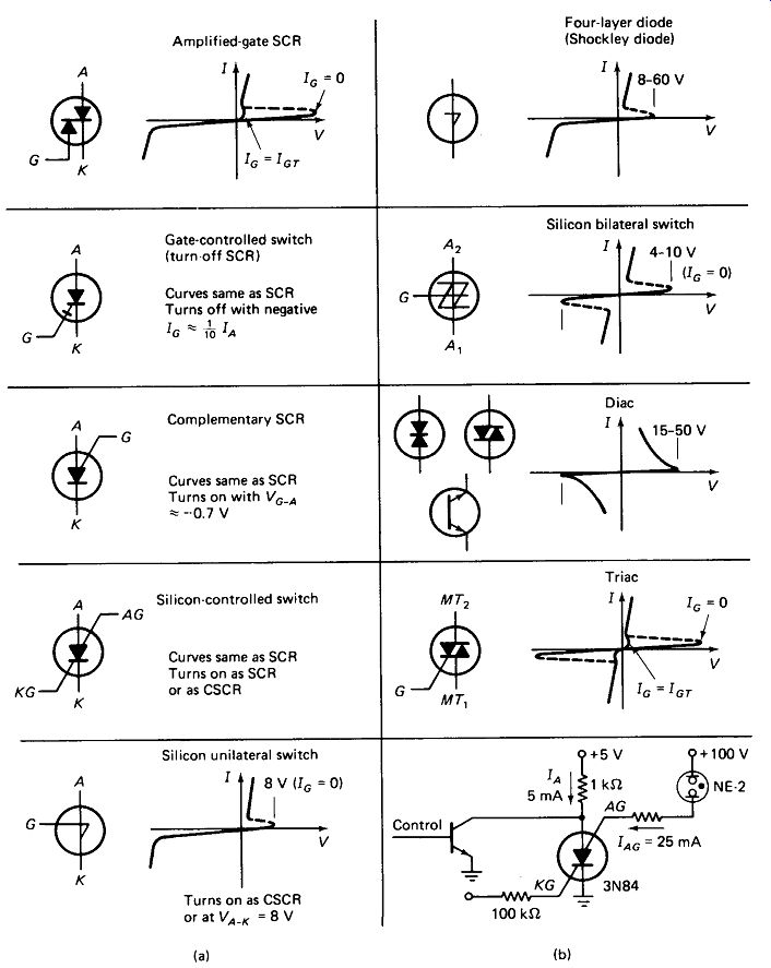
Fig. 9-15
Shockley or Four-Layer Diode: This device is similar to the SUS and finds similar applications. It has no gate control and is available in a range of breakdown voltages from 8 to 60 V. It is faster than the SUS, switching in about 0.1 fis.
Silicon Bilateral Switch: The SBS is a parallel connection of two oppositely facing SUS devices. It triggers at the specified voltage in either direction if the gate is left open, but can be triggered earlier by a negative voltage from the gate to the currently positive anode. Self-triggering voltages from 4 to 10 V are common.
Diac: This is a three-layer silicon trigger device similar to SBS but without a gate lead. Commonly available trigger voltages range from ± 15 to ±50 V. The device voltage does not necessarily drop to a low value upon triggering, but " switches back" at a specified rate AV/AI as shown in Fig. 9-15. There seems to be quite a fight over what symbol to give the diac, so all three contenders are shown in the figure. The primary use for the diac is as a trigger for a triac.
Triac: As the name implies, the Triac is a three-lead device designed to handle ac.
It might also be called a bidirectional SCR, because that is exactly how it functions. The Triac can be triggered by either a positive or negative voltage from gate to main terminal 1 for either a positive or negative voltage on main terminal 2.
The four triggering modes are referred to as the four quadrants of the Triac, from a presumed graph of IMT2 versus IGMTt, as shown in Fig. 9-16. Such a graph is seldom given in practice, but the concept helps keep things straight. Some manufacturers refer to quadrants 2 and 4 as I - mode and III + mode, respectively, so these labels are given, too. Triggering current IGT is quite different for the various quadrants, being generally lowest in quadrant I and highest in IV. Where a single polarity of gate trigger pulse is used to trigger on both polarities of the line, negative gate pulses are generally used to avoid the high current demand of quadrant IV and the inequality between quadrants I and IV. Some Triacs are not guaranteed to trigger at all in quadrants II and IV. Gate voltages and currents, on-state voltage, and response times for triacs are similar to corresponding values for comparable-size SCRs.
Triac Applications: Figure 9-17(a) shows an elementary Triac light dimmer. With R2 at maximum, Vc lags the line by about 85°, but never becomes large enough to trigger D, and the Triac remains off. As R2 decreases, Vc increases, until at its peak (84° + 90°) it is high enough to trigger D and fire the triac. The line voltage now appears across the lamp, the RC voltage being clamped to zero by the triac. The capacitor voltage thus drops as the diac discharges it, and holds until the negative half-cycle of the line, when the triac turns off and voltage again appears across RC.
The discharge of C by the triggering of D has brought Vc nearer to its next (negative) triggering point, however, and triggering occurs quite a bit earlier than it did on the positive half-cycle, as shown in Fig. 9-17(b). The negative trigger likewise brings Vc nearer to the positive trigger level, resulting in conduction angles ...
FIGURE 9-16 Triac symbol and the two competing systems for naming the four
possible firing modes. Note representative magnitudes of firing current I_G
in each mode.
... between 30° and 40° per half-cycle. Rotating R2 thus produces nothing at first, until the lamp suddenly pops on at about one-tenth brightness. Backing off on R2 then produces lower brightness. This effect is called hysteresis.
Figure 9-17(c) shows a simple way of reducing hysteresis to an insignificant level. R} and C2 provide isolation so that C1 is not seriously discharged when £), triggers. R3 and C2 also provide an additional 20° lag in triggering voltage so that *C2 is on a steeper rise at the point of trigger.
Switching a Triac or SCR on in the middle of the ac half-cycle causes very abrupt current changes which produce interference in nearby AM radios. The circuit of Fig. 9-17(c) has a hash filter LXC3 to suppress this.
Figure 9-18(a) shows a simple scheme for eliminating sparking and pitting when switch contacts are used to control an inductive load. The 1-k-Ohm resistor turns the triac on near the beginning of each half-cycle (or in the middle of a half-cycle if the switch is closed then), but when the switch is opened the Triac waits until the current alternates through zero before turning off.
Figure 9-18(b) shows a scheme for turning the power on and off only at the zero-voltage crossings of the ac line. The initial current inrush to a cold lamp filament is 5 or 10 times its hot-filament value, so the thermal shock if the switch happens to close when the line is near its peak voltage is quite severe. Synchronous switching at the zero-voltage point thus extends lamp life, and if the lamp is part of a flashing sign on an 80-ft pole in midwinter, the cost of the circuitry will seem amply justified. R1, R2, and D1, feed turn-on current to the gate of the Triac on positive half-cycles. The 3-mA IGT is reached at about 25 line volts. However, if the switch is closed, R1, D2, and R3 provide the 2-mA IGT for the SCR at about 12 line volts, firing the SCR and diverting the Triac gate current. D3 and R4 charge C on positive half-cycles if the Triac fires, and Z>4 discharges C through the Triac gate on the subsequent negative half-cycle, providing quadrant IV triggering. Rs speeds the turn off of the Triac at the zero-voltage crossings.
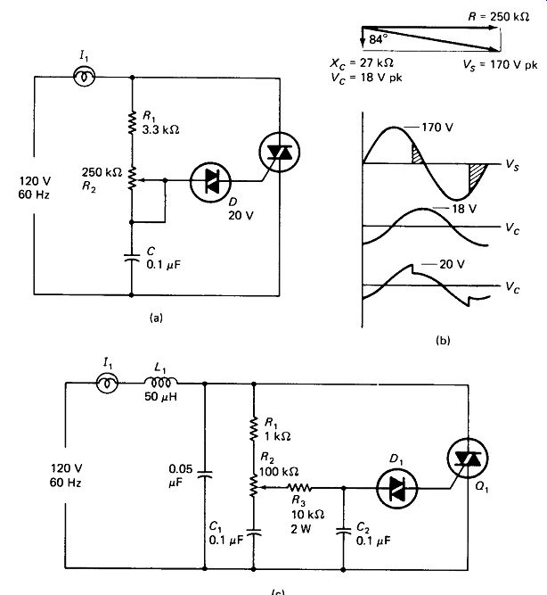
FIGURE 9-17 (a) Simple triac trigger using a disc and single RC phase-shift
network, (b) Phase-shift diagram and waveforms at threshold of tiring. Indicating
cause of " pop-on " hysteresis, (c) Two-RC network with diac trigger
minimizes hysteresis.
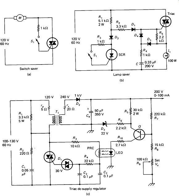
FIGURE 9-18 (a) Turning off an Inductive load at the zero-line-voltage point
to avoid kickback, (b) Turning a lamp on and off at the zero-line-voltage
points to minimize thermal shock, (c) High-voltage regulated supply using
a triac on the low-voltage side of the transformer and optical coupling to
the trigger circuit.
Figure 9-18(c) shows a Triac solution to the problem of regulating high-voltage power supplies. Consider a 3000-V 1-A supply for a medium-power radio transmitter. Assuming a ±15% line-voltage Variation, we would require a 900-V 1-A series pass transistor and a 900-W heat sink using conventional techniques.
By regulating on the primary rather than the secondary side of the power transformer, we can get by with a 350-V 12-A Triac on a 25-W heat sink. The circuit shown and tested is somewhat more modest because of the cowardice of the author, but the same principles are evident.
R1 supplies hold-on current for the triac after the brief charging pulse of rectifier D2CA is over. R2 and C, form a snubber preventing false triggering of the Triac. R3, C2, R4, C3, and Z>, form a triggering-delay network as in Fig. 9-18(c), except that the Variable resistance is a photoresistive cell driven by an LED which senses the output voltage. R5 and D3 fix the emitter voltage of Q while R6 provides degeneration to prevent self-oscillation. R7, Rs, and R9 form a voltage divider applying a fraction of VQ to the transistor base. If the output voltage drops, because of added load or drop in line voltage, VB drops below VE, turning Q more on, lowering the resistance of the PRC and increasing the triac conduction angle.
Output ripple is 30 V p-p at full load for this circuit, so an LC filter may be required between C4 and R5. Full-wave rectification would be of no avail because the triac inevitably triggers a bit earlier on the positive half-cycle, and the charge held on C4 obscures the smaller pulse from the negative half-cycle. A filter choke between D2 and C4 could eliminate this problem, but its value must be kept small and the load current must not drop near zero if regulation is to be maintained.