
By J. A. "Sam" Wilson, CET
NOR gates, EXCLUSIVE OR gates, six trouble shooting questions, and two digital experiments are covered this month. Also, details are given about using NAND and NOR gates to produce NOT gates.
NOR Gate
With NOR gates (Figure 1), the only way of obtaining a logic 1 output is to have logic 0 at both inputs. All other combinations of inputs produce a logic 0 at the output. The NOR formula is derived from: NOT A OR B EQUALS L.
NOR gate symbols are the same as those for OR gates, except for an indication that the output is inverted. In the MIL symbol, the small circle at the output shows inversion.
This is an important point, because it hints that a NOR gate can be constructed from an OR gate followed by an inverter (NOT gate).
In the basic industrial circuit, the normally-closed relay contact is energized (logic 1 at the load) only when both switches are open (logic 0). When either or both switches are closed, the relay opens the contact, producing a logic 0 at the load. This is in agreement with the truth table.
The math formula is read: NOT A OR B EQUALS L. The overbar must be across both the A and B, or the equation is written incorrectly.
Changing a NAND to a NOT
In the February article, I said that any of the basic logic gates could be constructed, if a sufficient number of NANDs (or NORs) is used. In other words, specific wirings of the NAND gates can produce any of the basic gates that we have described so far. The same is true of NOR gates.
It's easy to wire a NAND gate so it performs as a NOT (inverter), as shown in Figure 2. The two inputs are connected together; therefore, both inputs always have the same logic level. A conventional truth table is used, except the two conditions when the inputs have different logic levels are not possible. In Figure 2, these entries are removed from the truth table, leaving only the one with both inputs at logic level 0 (producing a high output) and the other with both inputs at logic level 1 (for a logic 0 output). Whenever the output always is reversed from the input, the circuit is an inverter (or a NOT gate).
Changing a NOR to a NOT
A NOR gate also can be wired to operate as an inverter. Figure 3 shows the two entries of the truth table that are impossible when the two inputs are connected together.
The only valid inputs are logic levels 0 and 0, which produce a level 1 output, and logic levels 1 and 1, Producing a logic level 0 output. These characteristics fulfill the requirements for a NOT gate (inverter).

Figure 1 These are the four basic characteristics of NOR gates.
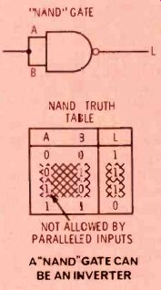
Figure 2 Connecting both inputs of a NAND gate together eliminates half
of the truth table, allowing it to function only as a NOT gate.
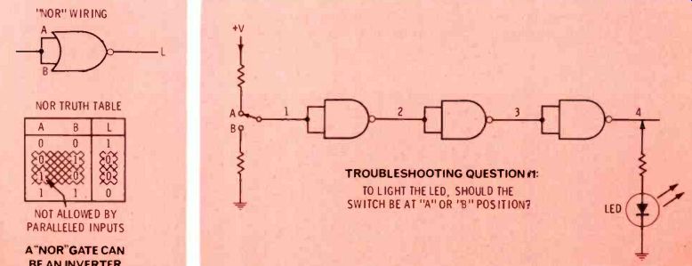
Figure 3 Connecting both NOR gate inputs together also eliminates half
of the truth table, leaving only the function of a NOT gate (inverter).
These last two illustrations prove that NOT gates can be constructed by connecting together the inputs of either NAND or NOR gates.
Troubleshooting
Question #1 Figure 4 asks a question about a series of NAND gates that are connected as NOTs.
What is your answer?
Troubleshooting Question #2
Answer the troubleshooting question of Figure 5, concerning two NOR gates connected as NOTs that feed the two inputs of another NOR gate.
Exclusive OR Gate
The symbols, truth table, basic circuit, and math symbols for an EXCLUSIVE OR gate are shown in Figure 6.
During a previous discussion of INCLUSIVE OR gates, we mentioned the two different meanings of the English word "or." When someone says, "John or Mary may go to the store," it could mean, "John or Mary or both may go to the store." This is the inclusive form. On the other hand, the intent might be to say, "John or Mary, but not both, may go to the store." This is the exclusive form of "or." The OR gate discussed in the January issue was the inclusive type where either or both of the inputs having a logic 1 produces an output of logic 1.
From the truth table in Figure 6, we learn that a logic 1 at either (but not both) input produces a logic 1 at the output. Another way of defining an EXCLUSIVE OR gate is that the inputs must be at opposite levels to obtain a logic 1 output. Notice that a plus sign is used both in the NEMA symbol and the first formula. In logic symbols, the plus sign indicates OR.
The basic industrial circuit needs some explanation. Two relays are provided, each with one normally-open and one normally-closed set of contacts. The normally-open con tact of M is in series with the normally-closed N contact. Also the normally-closed contact of M is in series with the normally-open N contact.
When neither relay is energized, no path exists through either pair of contacts (one normally-open is in each path). When both are energized, all of the contacts re verse, but still there is no path through the series contacts. The only way to light the lamp (logic 1) is to energize relay coil M or N, but not both.

Figure 5

Figure 6 Here are the basic characteristics of EXCLUSIVE OR gates.
Three-way switch
Let's analyze the operation of the so-called three-way lamp circuit of Figure 7A. It's used often to operate a hall lamp from the top or bottom of the stairs, or to control a garage light from the house or the garage.
With the light switches flipped as shown, the circuit is completed, and the lamp will light. Also, if both switches are flipped to the opposite positions, the circuit again has continuity (although through a different path) and the lamp is energized.
However, if just one of the switches is flipped, the power source and the lamp are connected to different wires. Therefore, the lamp does not light.
The logic of the circuit can be understood more easily, if the circuit is redrawn (Figure 7B) in industrial style similar to the basic circuit of Figure 6. The results agree with the truth table of Figure 6.
Troubleshooting Question #3
In Figure 8, given the B input level and the output level of the EXCLUSIVE OR gate, what must be the logic level at the A input?
Combinational Logic
Many logic circuits are made by combining gates. These are called combined-logic gates or combinational-logic gates. One example is shown in Figure 9. The two inputs of a NOR gate are tied together, making it function as a NOT gate, and it is located between the A input and one input of an OR gate.
The B input goes direct to the OR gate.
It's important that you determine what the output level should be, so you can know if it is operating properly or not.
There are several ways of deter mining the output logic level (one is by Boolean algebra, but it will not be explained now). Perhaps the easiest method is to draw up a truth table (see Figure 9). Write in all combinations of logic levels for the two inputs.
We know that a NOT gate inverts the state, so we can fill in the NOT A column, as shown in Figure 10. The original A column is not used anymore, because the NOT A and the B logic levels are the input of the OR gate. Next, knowing that the only way to obtain logic level 0 at the output is to apply level 0 to both inputs, we can complete the truth table (Figure 11). The last step is to ignore the column, and to use the A and B logic levels plus the output level.
Notice that the inputs and outputs were taken a step at a time starting with the NOR which is wired as a NOT, continuing on to the two inputs of the OR gate (allowing us to know the output, and finishing by going back to the original A and B inputs.)
Troubleshooting Question #4
Figure 12 shows the logic circuit of Figure 9, but both inputs are supplied with logic level 0. What level should the probe indicate at the output?
Troubleshooting Question #5
In the circuit with three NAND gates of Figure 13, what should be written in the blank spaces of the truth table? Experiment #1
This experiment is in two parts.
The circuit of Figure 14 shows a 7400-series IC containing four NAND gates that have beer wired to make them perform as NOT gates. First, use your knowledge of digital circuits, by completing the truth table at the left, both for an input of logic 0 and for logic 1.
Second, wire the circuit as shown.
Apply a ground (logic 0) to input A and use a logic probe to test each of the four points, writing down the logic states. Repeat the test with the A input connected to +5 volts (logic 1), and write down the other four logic levels, as measured by the probe, in the spaces of the truth table at the right.
Of course, the experimental results should be identical with the predicted performance.

Figure 7
This "three-way" lamp wiring (A) has been used for years. It is a practical example of an EXCLUSIVE OR gate. (B) Drawn in industrial style, the circuit is almost identical to that in Figure 6.

Figure 8
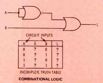
Figure 9 Logic circuits composed of two or more logic gates are called "combination
logic." A NOR gate is wired as a NOT, and it feeds one input of
an OR gate. From this information, compete the truth table.
Troubleshooting
Question #6: When you have completed the truth tables in Figure 14 (and both are the same), have you completely checked all of the NAND gates? Experiment #2 Construct the circuit of Figure 9.
Using a logic probe, measure the output when the inputs have the logic levels shown there. (Obtain a logic 1 by connecting the input to +5 volts of the power supply.
Simulate a logic 0 by connecting the gate to common of the power supply. Complete the truth table, trying each combination of inputs separately. The finished truth table should be identical to the one in Figure 11.
--------------
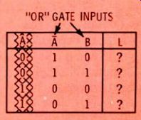
Figure 10 The NOT A column can be filled in easily, since the output
of an inverter al ways is opposite to the input.
As shown, this identifies the two inputs to the OR gate (NOT A and B inputs). From the information complete the output logic states.

Figure 11 After the OR output is determined, the NOT A column is not
needed. Use the A and B columns of the truth table as the inputs of the
combinational logic system.
------------
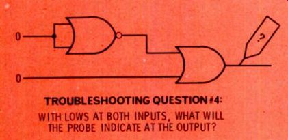
Figure 12

Figure 13
Answers to the Troubleshooting Questions
Answer #1. The switch of Figure 4 must be in the "B" position to produce a logic 1 at test-point 4, thus lighting the LED. The NANDs are wired as NOTs, so a logic 0 at point 1 produces a logic 1 at point 2, a logic 0 at point 3, and finally a logic 1 at point 4 for the LED.
Answer #2. The probe of Figure 5 should indicate a logic level 0. NOR gates #1 and #2 are wired as NOTs, which places a logic 0 at "A" and a logic 1 at "B" of NOR gate #3.
With inputs of 0 and 1, the output must be logic 0, which can be confirmed by the truth table of Figure 1.
Answer #3. The logic level at input "A" in Figure 8 must be 0, if the gate is operating properly. The output is level 1, and the inputs of an EXCLUSIVE OR gate must be opposite to obtain that result. In put "B" has logic 1; therefore, input "A" must be logic 0.
Answer #4. In Figure 12, the logic probe should show a logic 1 output.
The NOR gate has been wired as a NOT, making the inputs of the OR gate a logic 1 and a logic 0. This calls for a logic 1 output level, which can be verified by the truth table of Figure 11.
Answer #5. The completed truth table of Figure 13 is shown in Figure 15. That answers the question, but there's more. Eliminate the NOT A and NOT B columns, and the truth table that remains (Figure 16) is for an INCLUSIVE OR gate. An OR has been constructed from three NANDs! Other examples of gates made from combinations of other gates will be given next month.
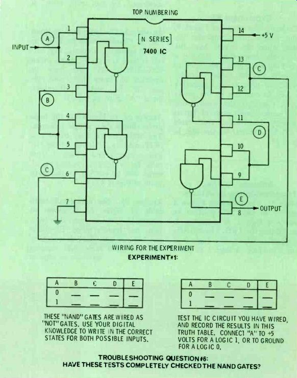
Figure 14
Calculate the truth table at the left. Then, con struct the experimental circuit and use a logic probe to deter mine the logic states at each point, filling in the truth table at the right. If the four NAND gates are not defective, the two truth tables should be identical.

Figure 15 This is the truth table of Figure 13, after it is completed.

Figure 16 (far right) After the NOT A and NOT B columns of Figure 15
have been eliminated, the truth table that remains is the one for an
INCLUSIVE OR gate. Therefore, three NAND gates have been wired to produce
an INCLUSIVE OR gate.
Answer #6. No, you have not completely checked all of the NAND gates. You have proved correct operation when both gates are switched together, but not with inputs of opposite logic levels.
However, it's likely that NANDs which pass this test actually are okay. Quick tests have value, but keep in mind that additional testing might be required (for example, to determine the propagation delay).
(adapted from: Electronic Servicing magazine, Mar. 1978)
Next: The Basics of Industrial Electronics, Part 10
Prev:
Also see: Sam Wilson's Technical Notebook