
By J. A. "Sam" Wilson, CET
Sam shows how Schmitt triggers can be obtained from NAND latches. Disallowed conditions of flip flops are explained, also experiments and troubleshooting questions are presented.
TTL IC Pinouts
The experiments of this article require TTL NAND gates. We will specify the IC number; however, the pinout numbering won't be listed.
As shown in Figure 1, many different pinouts have been used for the 7401 NAND-gate ICs, with the actual pinout identified by a letter or two after the IC number. We can't know which version you have.
Therefore, you must consult a TTL manual for the correct pinout diagram.
All TTL logic devices require a regulated 5-volt power-supply source, so be certain your supply voltage does not drift more than a few tenths of a volt.
More Uses for TTL
Latches NAND and NOR latches, such as the ones described last month, can be wired to operate as Schmitt triggers, and other useful circuits.
For Schmitt triggers, a D-type flip flop can be used.
D-Type Flip Flops
NAND and NOR latches are called "R-S flip flops." When such latches are wired with a new D input which feeds one input directly and the other through a NOT gate, the total circuit (Figure 2) is called a D flip flop.
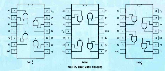
Figure 1 ICs with several gates often have more than one pin-out diagram,
as shown here for the 4-gate NAND IC. Therefore, the pin numbers won't be
given for later experiments.
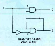
Figure 2 Adding a NOT to the R input of a NAND latch changes the circuit
to a type-D latch, that operates with pulses or square waves from a single
source.
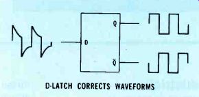
Figure 3 One advantage of D-latches is the ability to correct distorted
digital waveforms.
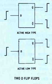
Figure 4 D-latches are available in either active high types or active low
types. The one in Figure 2 is an active low type.
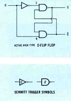
Figure 5 This is one possible way of constructing an active high type of
D-latch (flip flop).
Figure
6 The turn-on voltage of a Schmitt trigger is different than the turn-off
voltage. Therefore, the hysteresis symbol is used.
Last month, we pointed out that R-S flip flops never should have the same logic level at both inputs.
Identical inputs produce either a quiescent (inactive) or a disallowed output state. (Disallowed inputs cause an output that can't be determined with certainty.) Inversion of one input (by a NOT) prevents both quiescent and disallowed conditions.
A square wave at the D input of Figure 2 will result in a square wave at the output. Now, that doesn't seem like much of an accomplishment, but it also can produce good output square waves even when the input waveform is badly distorted.
For example, in Figure 3 the input signal has tilted square waves with overshoot (because of low-frequency attenuation), but the output waveform has perfect square waves.
This is an advantage of digital operation. The output at Q can be ONLY high or low. In fact, a proper sine-wave input produces square waves at the output.
Duplication of Terms
Digital gates often have many names. Usually a tech writer will use only one, to avoid confusion. However, you should understand all such terms.
For example, R-S flip flops have been called:
latch
memory latch
bounceless switch
SR flip flop (rare).
In the same way, D-type latches have been called:
D-type latch
D low latch
D high latch
D flip flop
Schmitt trigger.
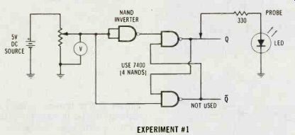
Figure 7
Construct this circuit to test the operation of D-type active high latches. Use your simple probe to determine the output state.
High and Low D Latches
Figure 4 shows the symbol for a D "high" latch (the output goes high when the D input goes high), and another symbol for a D "low" latch (the output goes low when the D input goes high).
Notice the small circle at the D input of the D low latch. In digital schematics, such circles indicate inversion. Therefore, a D high latch can be changed to a D low latch by adding a NOT gate at the D input.
However, if you are constructing a D latch from NANDs and NOTs, you can save one NOT gate by wiring the active high D flip flop as shown in Figure 5. Compare this to the active low D flip flop of Figure 2. The difference is whether the S or the R input has the inverter.
Schmitt Trigger
Schmitt triggers are fast-acting digital switches that change output state from low to high when the input signal rises above a certain voltage level. Therefore, the high D latch circuit of Figure 5 has the essential Schmitt trigger characteristics.
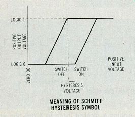
Figure 8 The Schmitt trigger symbol is a type of hysteresis graph, with
the input and output levels shown together. When the DC input voltage is
increased to the switch-on level, the output goes high (shown by the line
sloping upward-it's sloping because time is required). At the top, the horizontal
line extends to the right to show that further increases of input voltage
do not change the output voltage. Next, the input voltage is decreased (shown
by extending the line to the left) until the output goes low (line sloping
down to zero).
This switch-off input voltage is lower than the switch-on voltage. The difference between the two switching voltages is called the "hysteresis voltage."
Schmitt triggers can be constructed by several different methods. Even NOT or NAND gates can operate as Schmitt triggers. However, most Schmitt triggers in ICs have additional circuitry.
The symbol inside the NOT and NAND drawings of Figure 6 is the one most often used for Schmitt triggers, although it actually is the symbol for hysteresis. Hysteresis refers to any action that occurs at a different point according to whether an activating condition is increasing or decreasing.
In the case of Schmitt triggers, when the input voltage is increased gradually, the output suddenly will go high at one certain input voltage. Then, as the input voltage is decreased gradually, the output suddenly becomes low, but at a different input voltage than the one that caused the high. The next experiment demonstrates this hysteresis effect.
Experiment #1 The circuit of Figure 7 allows you to measure the input voltage that causes a high output from this D latch, and the decreasing voltage that switches the D latch output to low. The voltage difference between these two trigger points is called the hysteresis voltage. A simple LED logic probe is used to determine when the output is high (the LED is lighted).
Step 1 Starting at zero volts, slowly increase the input voltage by turning the potentiometer. Watch the voltmeter and the probe LED.
Notice and write down the voltage that triggers a high at the output.
Step 2 Increase the input voltage to +5 volts, then gradually decrease it until the LED goes dark. Write down the voltage at turn-off.
Conclusion
The voltages you recorded at turn-on and turn-off should not be the same (if you measured accurately and carefully). Because these voltages are different, the hysteresis symbol is appropriate for the Schmitt trigger.
Figure 8 shows how the hysteresis symbol is developed.
Experiment #2
The waveshaping characteristic of Schmitt triggers is shown by this experiment.
A 6.3-volt RMS heater transformer is used to supply a sinusoidal input voltage (Figure 9). 6.3 volts RMS is about 8.9 volts per peak. After rectification, each peak will measure 8.9 volts minus about 1.2 volts drop across the two diodes in series, or about 7.7 volts. This is too high for TTL gates, so you should begin with the voltage control turned down. Then, increase the signal voltage until it reads 5 volts peak-to-peak on a calibrated scope. If you don't have a calibrated scope, use a VOM or VTVM and adjust it for +3.6 volts DC (which will give about 5 volts PP for that waveform).
When the full-wave rectified voltage is applied to the D-type high flip flop, the output consists of square-tipped pulses, as shown in Figure 9. The output does not have square waves, because the input waveform is not symmetrical, and also the triggering point for turn-on and turn-off are not centered between zero and +5 volts.

Figure 9 Parabolic wave forms from unfiltered full-wave rectification can
be used as an input signal to an active high D-latch, producing square-tipped
pulses at the output.
Use your scope to set the control for 5 volts peak-to-peak, before you connect the D-latch.
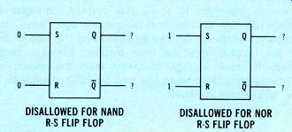
Figure 10 These are the disallowed input conditions for NAND and NOR R-S
flip flops.
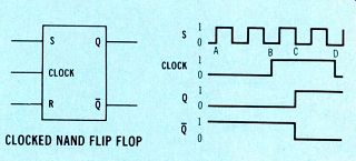
Figure 11 Adding a clocked input to a flip flop prevents false triggering.
Use a triggered-sweep scope to measure the rise time and the decay time of the output pulses. (Remember that the rise and decay times are measured between the 10% and 90% points of the pulse or square wave total amplitude.) Record the measured times here:
rise time was nanoseconds.
decay time was nanoseconds.
(Nano is exactly between pico and micro; so multiply microseconds by 1,000 to obtain nanoseconds.) IC D-type flip flops typically have switching times of 20 to 30 nano seconds. However, your D-type circuit might have slower switching (more nanoseconds) because of added stray capacitance.
Clocked Flip Flops
One disadvantage of RS flip flops is that certain combinations of inputs are disallowed. In this case, "disallowed" doesn't mean it's impossible, but that it's not advisable.
Different flip flops react in various ways to these wrong inputs. One might have a flurry of output highs and lows before settling down to a steady high or low output. But the output state is not predictable; it might be either high or low. Some flip flops draw extra current and destroy themselves. Regardless of the results, you should not deliberately cause a disallowed condition.
As shown in Figure 10, NAND R-S flip flops never should have lows at both inputs simultaneously, and NOR R-S flip flops should not have highs at both inputs.
NAND flip flops normally have highs (logic 1) at both inputs during the stable states, and the appropriate input is switched low momentarily to change the output condition. NOR flip flops are just the opposite; the inputs have lows, and one input is switched momentarily to high.
When R-S flip flops are stable in either a high or a low output condition, they remain steady until the proper input signal is delivered to the appropriate input terminal.
However, a noise signal at the input, or an accidental input from some source that is not supposed to trigger the flip flop, can cause it to change condition. Any triggering at the wrong time is very undesirable.
To prevent accidental triggering, a clock input terminal can be added to a flip flop, as shown with a NAND in Figure 11. (NANDs are triggered by a low at the proper input terminal.) At the beginning, the flip flop is in the low condition, with a 0 at Q output and a 1 at 'the Q output. Before it can be triggered to a high condition, a high must be applied to the clock input and a low applied momentarily to the S input.
Digital square waves are at the S input, thus furnishing a series of highs and lows. But none of the lows can trigger the flip flop. That is, not until the clock input first is high. Only then can the next low at the S input trigger the flip flop to the high condition.
Between time point A and point B of the waveform, the flip flop is forced to remain in the original low condition, because the clock re mains low. Then at point B, the clock signal goes high. However, the flip flop still can't change because the signal at the S input is low (remember NAND flip flops can change only when the input signal goes from 1 to 0). At point C, the S signal goes low, and the flip flop changes to high, with a high at Q and a low at Q.
The clock signal returns to low at point D; however, the flip flop re mains in the high condition. In fact, it will remain high until the R input is switched to low while the clock input is switched to high.
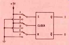
Figure 12 Troubleshooting Question
#1: Assuming that the clock input must be high for triggering to occur, how should you adjust the input switches to produce a low output from the clocked latch?
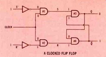
Figure 13 This is one method of constructing a clocked flip flop, using
NANDs.
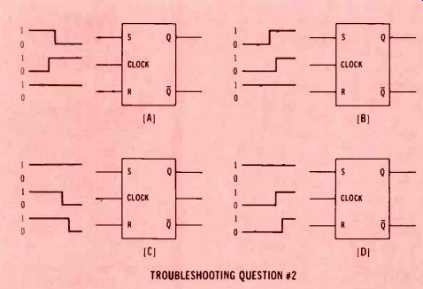
Figure 14 Troubleshooting Question #2: Given these input conditions, what
should be the output state of each clocked flip flop?
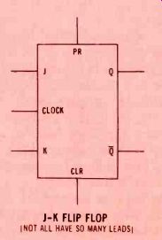
Figure 15 J-K flip flops do not have any disallowed input states. Some versions
have fewer pins.

----------- Two schematics were reversed in Figure 2 of page 52 in the
May issue of Electronic Servicing. The two figures are correctly reprinted
here, in the original size. You can cut them out and paste them over the
wrong ones, if you like.
Figure 1 An AND gate followed by a NOT gate becomes a NAND. The math formula for AND gates is read, "A AND B = L." The NOT gate at the output negates that so it reads, "NOT A AND B = L." As shown in the drawing, the overbar should cover both letters and the expression which is in between. (It might be more clear written "NOT (A AND B) = L.")
Figure 2 Inverting both inputs of an AND gate does not produce a NAND gate (notice the differences in the truth tables). Instead, it is another way to construct a NOR gate. The formula is read, "NOT A AND NOT B = L.
Remember: NOT A AND B = L isn't the same as NOT A AND NOT B = L.
----
Troubleshooting
Question #1
The R-S flip flop of Figure 12 is in the high output condition. How should you flip the three switches to trigger a change to the low condition? Assume that the clock must be in a logic 1 (high) condition to allow the flip flop to change.
----
Adding a Clock
Figure 13 shows one way of adding a clock input to a R-S flip flop. NANDs #3 and #4 are the two cross-coupled gates making up a R-S flip flop. Additional NANDs #1 and #2 are added to control the R and S inputs.
Remember that a logical low (0) at either or both inputs of a NAND automatically produces a high (1) output. So, the outputs of NANDs #1 and #2 will be logic 1 so long as the clock input is maintained at a 0 input.
The true inputs to the circuit are at S' and R', and they are inverted by the NOT gates before reaching NANDs #1 and #2.
Except when the condition of the flip flop is being changed, the S' and R' inputs normally are maintained at logic 1. Therefore, both inputs of #1 and #2 are at logic 0.
The flip flop is in the low condition, as shown, so switching the clock to logic 1 places a 1 at both clock inputs of #1 and #2. If S' now is switched to 0, there will be two l's at the input of NAND #1, therefore, the output will switch to 0.
NAND #3 now has a 0 input from NAND #1 and a 1 input from the 0 output terminal, causing a 1 output at Q. NAND #2 has not changed (a 0 and a 1 give a 1 output, just as the previous 0 and 0 did). NAND #4 has a 1 from the Q output and a 1 from the output of NAND #2, so the output changes to 0. The clocked flip flop now is in the high condition.
Telling all of these actions in sequence requires much time, but the switching time from the first input change to the stable high output requires about 20 nano seconds (0.00000002 seconds) for TTL logic systems.
--- ----
Troubleshooting
Question #2
What are the R-S flip flop outputs of Figure 14? The S R terminals are not marked with primes now, as they were in Figure 13, for they are considered to be the inputs to the clock flip flop. Assume that the flip flop is in a low condition when the switching signals arrive, and that a logic 1 must be at the clock terminal in order for the flip flop to change condition.
--- ----
The J-K Flip Flop
The most versatile of the IC flip flops is the J-K type. (The letters J and K have no, special meaning.)
J-K flip flops do not have any disallowed input conditions. This improvement is possible by using one R-S flip flop to switch another. The schematic symbol of J-K flip flops is shown in Figure 15.
The two R-S flip flops in the J-K type are called the master and the slave, with the slave connected to the output terminals. Also, the preset (PR) and clear (CLR) terminals predominate. A logic 0 delivered to the PR terminal places the flip flop in the high condition, regardless of the logic levels at the other terminals.
We'll take up J-K flip flops in more detail next month, and also describe a simple counting circuit.
Answers to Troubleshooting Questions
Question #1
To change the flip flop to a low condition, the S switch of Figure 12 should be high (as shown), the clock switch should also be high (as shown), and the R switch momentarily should be switched to low (position F of the R switch). One reason for this specific sequence is to avoid disallowed conditions. For example, if S is low when R is switched to low, then both would be low simultaneously; and that's a no-no. So, it's best to keep them both high between switchings.
Question #2
The A flip flop of Figure 14 will switch to a high condition. The B flip flop will re main in a low condition. The C flip flop will stay in the low condition.
The D flip flop will stay in a low condition.
(adapted from: Electronic Servicing magazine, Jun. 1978)
Next: Part 13
Prev:
Also see: Sam Wilson's Technical Notebook