Timers, Clocks, and Toggled Flip Flops
By J. A. "Sam" Wilson, CET
Most versatile of all flip flops is the J-K type, which was introduced last month in this series. One important application for J-K flip flops is in electronic counters. But, before electronic counters, we must consider electronic timers.
Electronic Timers
Usually, we think of timers as mechanical or electronic devices (such as a clock radio) that are used to start or stop an operation of some kind. And, these devices are used extensively in industrial electronics. The electronic or mechanical timer of a spot welder, for example, controls the length a time that the current flows, to insure proper bonding of the metals.
Many home appliances have timers. Each automatic washer has an electro/mechanical timer that controls the minutes of each cycle.
Where only a single on/off or off/on cycle (or a continuous series of identical cycles) is needed, an electronic timer can do a better job by allowing shorter or longer timed periods and accurate repeatability.
For photographic purposes, some electronic photo timers offer a selection of times from 0.1 second to several minutes. However, in digital circuits, a timer usually is a "clock," which is a square-wave or pulse generator.
The 555 IC is very popular for various kinds of electronic timers.
It can produce a single on/off cycle of any time up to several hours, or continuous square waves with rise times of 100 nanoseconds. This rapid rise and decay time makes the 555 able to function efficiently as a generator of clock signals for counting and display circuits.
The 555 Timer A square-wave generator is our first application for the 555 timer IC.
Other IC timing devices and an in-depth study of the 555 can be found in the IC Timer Cookbook, by Walter G. Jung (Howard Sams book number 21416).
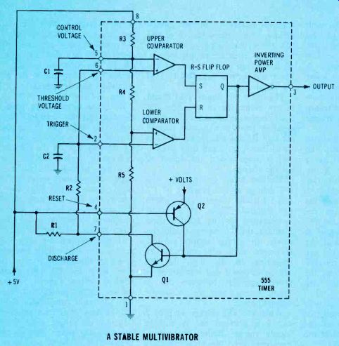
An astable multivibrator circuit using a 555 IC is shown in Figure 1. The word "astable" indicates the circuit has no stable state. In other words, it is a free-running multi-vibrator oscillator. Many tube oscillators of similar basic principle were used in the vertical and horizontal sweep circuits several years ago.

Figure 1 The 555 timer IC is versatile.
When wired this way, it becomes a multi-vibrator (time-constant) oscillator, with an output that's compatible with TTL circuits.

Figure 2 Op-amp symbols are used also for voltage comparators. When voltage
at the "A"' input is more positive than the voltage at "B",
the output goes low. Conversely, when the "A" voltage is less positive
than the voltage at "B", the output goes high. This is illustrated
by the waveforms, which are shown with the correct phase between input and
output.

Figure 3. The sawteeth are shaped by C2, and they are connected to pins 2
and 6. The square-tipped pulses are the waveform at pin 3, the IC output.
Remember, the flip flop output state and the IC output state are opposite.
T1 begins when the lower comparator drives the flip flop output low. During
`1, the flip flop output remains low. At the end of Ti, the upper comparator
triggers the flip flop to a high output. This starts T2 During T2, the flip
flop output remains high. At the end of T2, the output of the flip flop is
driven low again. This is the end of one cycle of operation, and also the
beginning of a new T1.
Inside the 555
The dotted lines of Figure 1 enclose the internal circuitry of the 555 IC, while the external components allow the timer to operate as an astable multivibrator oscillator.
(However, if pin 2 is disconnected from pin 6, the circuit can't oscillate continuously. Instead, the pin 3 output state will reverse each time a negative-going pulse is applied to pin 2. This is called "monostable" operation.) The values of the R1/R2/C2 time constant determines the free-running frequency of the oscillator.
Capacitor C1 is not essential for many applications, although it does minimize the possibility of noise triggering the multivibrator.
Two voltage comparators are in the IC. The output state of a voltage comparator changes according to which input has the highest voltage. Some comparators are merely operational amplifiers (op amps) that don't have any feedback to reduce the gain. In fact, the op amp and- input identifications sometimes are used also for voltage comparators, as shown in Figure 1.
Where used, the "-" indicates the inverting input, and the + is for the non-inverting input. In such cases, the output state of the comparator is low when the input has a higher positive voltage than the + input has. Also, the output is high when the - input has a lower positive than the + input has. Because of the very high gain, only a few millivolts of voltage difference between the two inputs can trigger an output change of state.
Figure 2 shows one way to operate a voltage comparator. The B (or + non-inverting) input has a fixed DC voltage, and the A (inverting) input has a triangular waveform. When the triangle voltage rises above the DC voltage, the output goes low. And when the triangle waveform is below the DC comparison voltage, the output is high. These relationships and the corresponding output states are shown by the drawing. If the DC voltage had been centered on the triangles, the output would have been square waves.
Notice that the output has only the usual two digital states: high or low. Reversing the signals at the inputs also reverses the state of the output pulses or square waves.
The 555 as an oscillator
Returning to the circuit of Figure 1, one input of each comparator receives a fixed amount of DC voltage from the R3/R4/R5 internal voltage divider. The - input (pin 5 of the 555 IC) of the upper comparator has about 2/3 of the supply voltage, while the top (or +) input of the lower comparator has about 1/3 of the supply voltage.
The other two inputs (pins 2 and 6) are connected in parallel, and both receive a varying DC voltage coming from the power supply through R1 and R2. However, C2 is wired from pins 2 and 6 to ground, and it slows down the speed of voltage change.
Without either comparator, the DC voltage at the junction of R2 and C2 would be zero when power was applied. Then, at a speed determined by the R2/C2 time constant, the DC voltage would rise slowly up to the supply voltage.
However, with the comparators triggering the flip flop, the DC voltage at pins 2 and 6 is forced to move regularly between the 1/3 supply voltage and the 2/3 supply voltage points.
When the DC voltage at pins 2 and 6 is between the 1/3 and 2/3 supply voltage limits, both comparators have identical outputs (necessary to keep the flip flop in a stable low state). Let's start analyzing the cycle with the C2 voltage rising at 1/2 supply voltage. When it rises a few millivolts above the 2/3 supply voltage at the other input, the upper comparator switches to the opposite state, triggering the S input of the flip flop, and causing the flip flop output to go high. Part of this high is inverted by the power amplifier, and it appears as a low at pin 3 of the IC.
Also, the output high from the flip flop supplies forward bias for transistor Q1, and it conducts heavily as it begins to discharge C2 through R2. As the C2 voltage decreases slightly below the 2/3 reference voltage at pin 5, the upper comparator reverses the S input state of the flip flop. Of course, the flip flop does nothing; this step is necessary to prevent a disallowed condition when the R input is changed later.
If not stopped by some other action, the C2 voltage eventually would be discharged to zero. however, when the C2 voltage drops slightly below the 1/3 reference voltage (at the junction of R4 and R5), the lower comparator changes output state, thus resetting the flip flop to a low output state. In turn, the inverting power amplifier supplies a high to the IC output at pin 3.
Also, the low output of the flip flop at Q removes the Q1 forward bias, and stops the bleeding of the C2 charge by the Q1 conduction.
This allows the C2 voltage to begin rising again. As the C2 voltage rises slightly above the 1/3 reference voltage at R4/R5, the lower comparator reverses the output state, and with it the state of the flip flop R input. This is the end of one operating cycle. Of course, the cycle is repeated over and over again, as long as power is supplied to the IC, thus the 555 timer is functioning as a continuous oscillator.
Figure 3 gives the waveforms of the 555 multivibrator, along with the formula for the C2 charge and discharge times. Notice that the ramp portion of the sawtooth requires more time than the retrace portion, because the charging of C2 is done through both R1 and R2, while C2 is discharged through R2 only.

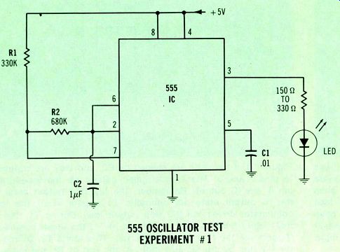
Figure 4 To make a digital clock for the experiment, wire the 555 IC with
these values.

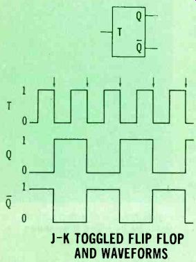
Figure 5 These waveforms of a J-K toggled flip flop prove that the toggle
is triggered by the falling side of the input (notice arrows), and that the
toggling acts as a divide-by-two.

Figure 6 (at right)--This is the pinout diagram of the 7446 IC, which has
two separate J-K flip flops.
However, the flip flop and the power amplifier can have nothing but high and low states. The output at pin three consists of square- tipped pulses (because the charge and discharge times are not equal), which are satisfactory for TTL operation.
Don't be misled by the output "power amplifier." It is not a high-output amplifier, since the entire 555 IC only draws about 200 milliamperes at 5 volts. However, the output is sufficient to operate LEDs.
In practical circuits, C2 can be an electrolytic type, when a low repetition rate is wanted. The resistors should be rated at % watt, or larger.
Experiment #1
Construct the astable multivibrator of Figure 4, using these values:
680K for R1, 330K for R2, 1 microfarad for C2, and .01 for C1.
Calculate the values of time 1, time 2, and time 3. Write the figures at the edge of Figure 4. You should obtain about 0.7 seconds for time 1, about .23 seconds for time 2, and about .93 seconds for time 3.
Measure the time of one complete cycle (time 3) by watching the LED in the circuit you have constructed.
Toggled Flip Flops
J-K flip flops are valuable be cause they can be toggled, as shown in Figure 5. The symbol is that of a toggled flip flop. However, it might be a J-K flip flop which has been wired in a specific way. Either square waves or square-topped pulses should be applied to the toggle terminal (T).
As stated before, TTL flip flops trigger at the trailing edge. In Figure 5, the trailing edges have been marked with arrows. Each time a trailing edge appears at the toggle terminal, the output changes state. However, notice that the Q output at the first arrow changes from 0 to 1, while the change is from 1 to 0 at the next arrow.
The output repetition rate at the Q output is exactly half of that at the toggle terminal. That's why this operation is sometimes called a divide-by-two.
A popular IC is the 7446, which has two separate J-K flip flops in a 16-pin DIP package. The pinout is given in Figure 6.
When used as a normal J-K flip flop, each section of the 7446 can be triggered to a high condition by a low at the preset terminal. And, a low at the clear terminal drives the flip flop to a low condition. Obviously, the preset and clear never should be allowed to have lows at the same time. These terminals are the equivalent of the set and reset in a R-S flip flop.
The Figure 6 pinout shows a common B+ and a common ground for the two flip flops. Otherwise, the two flip flops can be operated independently. In other words, you can wire and operate one flip flop, but connect nothing to the other terminals.

Figure 7 A J-K flip flop can be made to toggle by wiring it as shown.
Don't ground unused terminals
The previous paragraph suggests an important point about practical logic wiring.
With vacuum tubes and transistors, it is good practice never to allow any terminals to float without connections. An unused grid in a tube usually was connected to cathode or ground. This prevented the floating element from picking up an undesired signal, or from developing a negative charge from swarming electrons.
Not so, with logic circuitry. DO NOT GROUND ANY OF THE UNUSED TERMINALS. For example, think of any logic device that has a Q and a 0 output. These terminals have signals of opposite polarity. If you grounded the 0 terminal because it wasn't being used, then sooner or later it would attempt to go high. A high terminal that's connected to ground is the same as shorting the supply voltage to ground through the IC. THE IC WOULD BE RUINED.
Toggling the J-K Figure 7 shows how to wire a J-K flip flop for toggling. The clock terminal becomes the toggle input; then the preset, clear, J, and K terminals are wired to the positive side of the power supply.
Notice that this wiring is not in contradiction to the previous advice about not connecting to any unused terminals, because these terminals are used.
CMOS J-K flip flops should NOT be wired for toggling by this method. In fact, it won't work for all types of TTL J-K flip flops. You should check the pinouts of each type, and observe the manufacturer's recommendation for wiring any J-K flip flop for toggling.

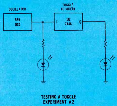
Figure 8 Combine the 555 multivibrator oscillator and one of the 7446 J-K
flip flops (which is wired to toggle) as an experiment to prove that a J-K
can be made to toggle.
Experiment #2
Earlier, the 555 IC timer was explained, and an experiment verified that it can operate as an astable multivibrator. In this experiment, the 555 multivibrator is used as a clock to toggle the J-K flip flop.
Both of these circuits were detailed before, so Figure 8 shows only a block diagram of the interconnections and the logic probes.
If you have wired everything properly, the second LED at the output of the toggle will flash at exactly half the rate of the first one.
If the first LED flashes too fast for good observation, parallel another capacitor or two across C2 until the flashes slow down.
Binary Numbering System
Until now, we have ignored the binary numbering system because it did not help explain the digital circuitry. Now, however, we must pause and learn the basics of binary counting. The next subject is about counters and display systems, which are designed to operate in the binary system.
People count by tens because the norm is ten fingers. But, there are other systems of counting. For example, many electronic devices have just two states of operation, such as on/off, saturated/not saturated, glowing/not-glowing, energized/not-energized, and many more. So, a system of counting by twos (binary) can be very useful.
Table 1 shows the decimal count from 0 to 15. The decimal system has ten individual symbols-one for each number 0 through 9. Then, when you reach the count of 9, all of the symbols are used up, and it's necessary to start a new column at the left. The new column uses the same ten symbols over again. To count up to decimal 15, then, two columns are required.
The binary system has only two symbols: 0 and 1. The first four columns are numbered 20, 21, 22, and 23, which correspond with the decimal numbers 1, 2, 4, and 8.
Later, you'll discover an important reason for identifying the columns in this way.
Patterns of the counts In the binary columns, the first number corresponding to decimal 0 also is 0 in binary (or 0000, for all four columns). The next number is 0001 for decimal 1. This has used up both symbols in the 2° column, so a new column must be started at the left, making 0010 for 2. Adding a 1 to the last column changes it to 0011 for 3. Next, a 1 is added to the 22 column, for a 0100 (or 4). It's followed by 0101 for decimal 5, and 0110 for 6, and finally filling the three columns, 0111 for decimal 7.
And so on, until the binary number is 1111 for decimal 15.
Did you notice the progressive pattern? In binary work, you will find it very helpful to identify this pattern.
The ones in these columns have decimal values, but at the beginning I suggest that you learn the pattern for counting. In a pinch, you can start with a number you know and write down the numbers in sequence until you reach the one you want.
Next Month: More information about binary counting and how to use toggled flip flops as frequency counters will be presented next month. If possible, keep the circuit of Figure 8 set up for the next experiment.
(adapted from: Electronic Servicing magazine, Jul. 1978)
Next: Part 14
Prev:
Also see: Sam Wilson's Technical Notebook