Magnetic Memories Store Digital Logic, and the Basics of Charge Coupling
By J. A. "Sam" Wilson, CET
Storing Digital Levels
In Magnetic Memories After several months spent re viewing magnetic principles, we're ready to apply some of them to the design of a simple magnetic memory for digital information.
Of course, computers and micro-processors use the same two levels of signal as do the digital-logic circuits explained in my industrial electronics series. The higher of the two voltages often is called "logic 1" or simply a "high." The near-zero voltage is called "logic 0" or a "low." Any device capable of attaining and holding two levels of operation can function as a memory. An on/off switch has only two levels of operation, the handle position is the readout, and it remains in the last state until forced to change again.
Many other devices have some type of memory.
Last month, we observed how a square-loop magnetic material will retain considerable magnetism, even after the magnetizing force has been removed. From that beginning, we'll show step by step how to store and retrieve digital signals.
Storing logic in magnetic cores Figure 1A shows the polarity of magnetism needed to store a logic 0, while Figure 1B illustrates the opposite polarity required for storage of a logic 1. Additional components are necessary before the flux can be changed and the state identified.
Proper flow of electron current in a winding around the magnetic material can produce the polarity of magnetism needed for a logic 0 (Figure 1C) and for a logic 1 (Figure 1D).

Figure 1. This is one method of storing logic 1 and logic 0 in magnetic
cores, according to the polarity of the flux. STORING LOGIC 0 AND 1 IN A
MAGNETIC CORE
A constant coil current is not required. The current can be turned on only long enough to produce the required flux, then it can be turned off. Pulses of DC current are one practical source of magnetization.
Of course, another pulse of the opposite DC current can reverse the magnetization, producing the other logic level.
Storage alone is not useful. The digital state of the magnetic material must be identified, and the method of determining the state must not change or erase the state.
Other components are needed.
Retrieving the information
Identification of the original flux state can be done with the addition of another coil to the coil/magnetic material assembly previously described. This added winding is called a "sensing coil." Figure 2A shows the magnetic material in the low state, with nothing connected to the two coils.
Electron current (of the same polarity as the current that magnetized it originally) is applied to L1. The magnetic flux does not change polarity. Therefore, a meter connected to L2 (as shown in Figure 2B) would NOT show a pulse of voltage. This is proof that the material previously was in the logic 0 state. The sensing current in L1 did not change the state of the flux.
So, no further action is needed.
Flux for the high state is shown in Figure 2C. When the same electron current as used in Figure 2B flows through L1, the original high flux is reversed to a low. The changing flux induces a voltage in the sensing coil, L2, thus proving that the original state had been a high. In other words, the method identified the high digital state, but reversed it in the process.
Notice that the magnetic material is in the low state after one readout, regardless of the original state. Obviously, the method has limited usefulness.
Figure 2 Addition of a sensing coil allows the previous logic 1 or logic 0 to be identified. Unfortunately, the sensing of a logic 1 reverses the flux to the logic 0 condition.
A solution
This undesired reversal of high states (lows are not affected) during identification tests can be corrected later by signal current in a third coil.
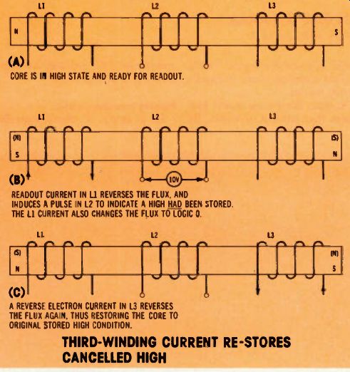
In Figure 3A, the core is shown in the high state. Readout current in L1 of Figure 3B reverses the flux, which induces a pulse in L2 (indicating the stored state had been a high). Reversing the flux changes the state to a logic 0. However, the logic I state can be re-stored by supplying a reverse flow of electron current through L3 after the readout has been made, as shown in Figure 3C. The method of Figure 3 is practical because a reversed logic 1 can be replaced by an opposite electron current through a third coil. Logic 0 states can be read without any reversal. Therefore, the circuit permits current through L3 only after a high has been read.
Circular cores
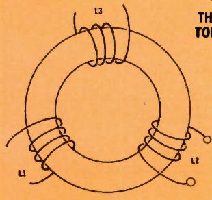
Less flux leakage and decreased pickup of hum and extraneous noise are obtained when the rectangular core of magnetic material is arranged into a toroid (Figure 4). The theory of operation remains the same.
More information about memories will be presented later.
Definitions???
Here are some electronic definitions sent to me by Mr. C. Jur of Los Angeles Valley College: Negative Charge-you pay them Positive Charge--they pay you Forbidden Gap-scene of a horse opera Junction--a fork in the road P/N Junction--a roadside rest area Energy Band-musicians who lift weights Semiconductor-a truck driver
Degenerate Semiconductor-truck driver who likes "tea"
Recombination --meeting the same people for the first time Dope-someone you know Heavily Doped -someone you wish you didn't know Stored Charge--a wine cellar Silicon--a foolish prisoner Base-the low man of a quartette Collector--a person who collects something Common Collector-a person who collects from everyone Emitter-an exit Common Emitter-the only door in the room Emitter Capacity -total number of people who can squeeze through a door at the same time Emitter Breakdown -the door collapsed Current Density -present stupidity Atom -part of the slang expression "up and atom" Delay Time-the time before an employee begins working after arriving at the shop Rise Time-the time after the alarm goes off before a person gets up Storage Time-accrued sick leave Fall Time-September to November DCTL-Don't Complain if the Transistor's Lousy
Switching Transistors-exchanging one transistor for another
Holes-the presence of nothing Hole Density -a concentrated amount of nothing in a small space Germanium -should have been a flower, but someone misspelled it.
This short course should have equipped you to talk electronic slang with anyone.

Figure 3. Addition of a third coil permits a high to be re-stored after
it is re versed by the readout current. No current is allowed in the re-storing
coil, except following the readout of a high. (Readout of a low does not
change the state of the core.) THIRD-WINDING CURRENT RE-STORES CANCELLED
HIGH

Figure 4 Practical magnetic cores have a toroidal shape that minimizes signal
leak age a- id core loss. THREE WINDINGS ON A TOROID HAS LESS LOSS
Faster Than a Speeding Bullet... An old news release tells of a circuit developed by the Bell Laboratory that could transmit one billion bits of information per second over a laser beam. That's one gigabit per second! If ever used in a continuous and practical application, the laser system could transmit 50,000 volumes of books in about 8 minutes. That's about 200 complete books transmit ted every second.
Of course, the system would just transmit that amount of words. By comparison, the printing of actual books is a slow process.
Printing invention needed In a study of electronographic printing, I learned several years ago that the limitation of being able to print at high speeds is the near impossibility of moving the paper through the machinery fast enough.
Paper is an insulator, and the friction of passing through the press generates a tremendous amount of static electricity. These high voltages interfere with the printing process, in addition to the bother of miniature lightning strokes playing around the press.
One of the most-needed inventions is a method of reducing static electricity charges during the high speed movement of paper. I'm passing this "pressing" need along to you, so you can become rich.
Now, I've always wanted to know someone who's rich. And, I presume when you receive great wealth from your invention, that you'll remember where you learned of the opportunity.
To prevent you from wasting too much time, here are some of the ideas that have been tried before.
One technique was to subject the paper to radiation produced by an atomic material. Another was to bombard the paper with ultra-violet light (or other rays) to neutralize the charges.
Of course, the paper could be made from a conductor rather than an insulator. But that's cheating, since it's not ordinary paper.
For relatively slow-moving paper, some presses have tinfoil strips attached to the press frame where they can contact the paper, and thus ground the static before it builds up to dangerous potentials.
After you develop and patent your solution to the static electricity problem, send me the details, and I'll print them in Technical Note book.

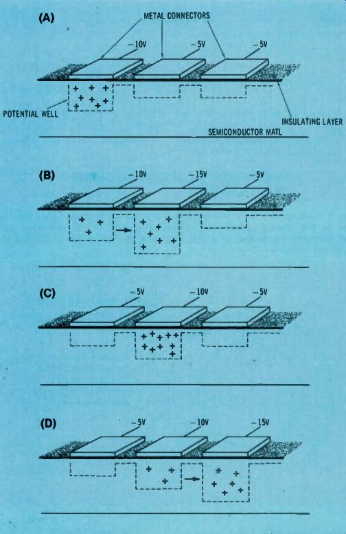
FIGURE 5 (A) The highest negative voltage at the first metal tab attracts
positive charges in the semiconductor material under the tab. (B) When the
DC voltages are changed as shown, the higher negative voltage at the second
tab attracts charges from the first tab (a process that requires some time).
(C) After all of the charges are moved over under the second tab, the DC
voltages are changed to a quiescent condition, with the highest negative
voltage at the second tab (to hold the charges there). (D) Applying the highest
negative voltage to the third tab causes the charges to move over under the
tab. After the charges are all under the third tab, the voltages are changed
to a quiescent condition with -5V at the first and second tabs, and -10V
at the third. The charges remain under the third tab until the voltages are
changed again.
Charge Coupling
Charge-coupled devices are mentioned frequently in news about electronic products. They have several important advantages over MOSFET and CMOS devices, and are certain to become very popular in the near future.
The model shown in Figure 5 consists of a semiconductor material with an insulating layer. Over the insulating layer are three metal tabs.
In Figure 5A, tab #1 (at the left) has a voltage of -10V, and the other two tabs each have -5V. The high negative charge applied to the first tab causes an accumulation of positive charges immediately beneath it. The potential barrier, which results from the negative charges of the tabs, is illustrated by the dotted line.
When the voltages are changed to -10V, -15V, and -5V, as shown in Figure 5B, the increased negative charge at the second tab forces the charges to move from left to right (as shown by the arrow). In Figure 5C, all of the charge carriers are presumed to have moved under the center tab, and the voltages are returned to quiescent values (the tab holding the charge has double the negative voltage). Notice that the potential well now is beneath the center tab. Motion of the charges from beneath one tab to the next was accomplished by changing the DC voltages, without any external current flow.
When the third tab voltage is changed to -15V, with -5V on the first and -10V at the second (see Figure 5D), the charges under tab two begin to move over to the right beneath tab three.
After all of the charges have moved to tab three, the voltages are returned to a quiescent condition, with -5V at the first two tabs and -10V at the third. (The higher voltage holds the charges there, until they are moved by a change of the voltages.) Of course, the process can be continued with more tabs at the right of these three, thus moving the charge carriers as far as the material and tabs extend.
Notice that charges have been moved from one area of a semiconductor material to another by a simple change of voltage at the tabs. External current, such as necessary with the collector or drain of transistors, does not flow. Obviously, current can be moved in charge-coupled devices by the use of less power than in other types.
A MOS device requires about 100 microwatts for each bit (a logic 1), while a charge-coupled device needs only about 5 microwatts per bit.
CCD devices can be operated at frequencies of about twice that possible with MOS devices.
Charge-coupled devices require only one-third to one-fourth as much area for each bit handled. Also, the physical construction of CCDs is much more simple than for either bipolar or CMOS devices.
In summary, charge-coupled devices surpass MOS ones in four areas: lower power; wider band width; smaller size; and simpler construction.
Three phase
The term "three phase" some times is associated with charge coupled devices. Think about that as you examine the operation of Figure 5 again. Imagine that the signal at each of the tabs is a varying voltage which is out of phase with the other two by 120 degrees. This is the phase between the three voltages of a 3-phase network. So, applying a 3-phase voltage to a series of tabs forces the charges to move along the material.
Applications
One of the first CCD applications was in a "bucket brigade," which moves bits of logic 1 and logic 0 information through a device in a series of tiny steps. In Figure 5, the tab with the accumulation of charges could represent a logic 1, while a tab without any charges might represent a logic 0. Bucket brigades are used as delay devices, because each step takes a definite amount of time, and many steps can be furnished in an IC. Another application for bucket brigades is in IC memories. Of course, memories store logic 1 or logic 0 levels, and the tabs of Figure 5 can hold a voltage almost indefinitely. The efficiency can be very high, since no external current is required either for programming or reading-out such memories.
We anticipate that charge coupled devices will become very popular in the near future.
------------
(adapted from: Electronic Servicing magazine, Aug. 1978)
Next: Sept. 1978
Prev: Link |
Also see: