By Jack Webster
Additional information is presented about digital memories of the type used in microprocessors. Also described are the connections and manual switching necessary for storing and reading-out a 7-digit phone number.
The cell array of the Figure 1 memory consists of 32 horizontal rows and 32 vertical columns, with a memory cell located at each intersection of a row and a column (see Figure 2). Actually, each cell is a flip flop which can memorize a digital high (1) or low (0).
Therefore, every cell has an address (location) that is identified by the intersection of a specified row and a specified column. In Figure 2, for example, memory cells are pointed out at A3, B4 and other addresses.
Because there are 32 rows and 32 columns, a total of 1024 cells is obtained by multiplying 32 times 32. Consequently, as many as 1024 bits (binary digits) can be stored in the memory that's traditionally called a 1K memory.
If 64 rows and 64 columns are provided, the total is 4096 cells for a 4K memory.
Addressing each cell
Each individual cell must be accessible during addressing so it's possible to write data into the cell.
Similarly, it's necessary to address each cell to read the digital high or low data that is stored in the cell.
If individual wires were used for each cell in Figure 1, a total of 1024 wires would be required for writing and reading all of the cells.
Obviously, such a large number of addressing wires is not practical, especially since most memories have many more cells than 1024.
However, Figure 1 shows only five row-selector inputs and five inputs to the column selector. This large reduction of the number of addressing wires is made possible by devices called decoders which convert the five inputs to 32 individual address lines.
Operation of a simple 2-input decoder is illustrated in Figure 3, where two inputs produce four individual addressing lines. The same general principle is used in larger decoders having five inputs and 32 output lines.
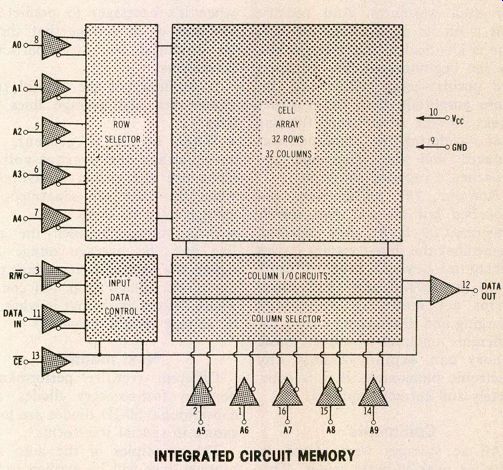
Figure
1 This 1K digital memory is similar to the type used in microprocessors. It
has 32 vertical columns and 32 horizontal rows for a total of 1024 memory
cells.
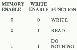
TRUTH TABLE
Read/write memory
Figure 4 shows an example of a read/write memory chip. Incidentally, the term random-access memory (RAM) usually is used instead of read/write. The IC is a TTL-type 7489 which can be wired to store and retrieve any telephone number.
The following truth table shows how the 7489 memory IC is programmed to store a number (write enable) or to read back the number (memory enable).
A few examples will show how a phone number (perhaps your office or home number) can be memorized and retrieved. The phone number for the example is 482 9046.
Storing digit 4
To store the first digit (decimal 4) in the first row, the select inputs are switched to 0000, which selects the first row for the storage mode.
Next, the actual number 4 is changed to binary 0100, which is entered into the data inputs terminals. (Of course, only binary digits can control electronic memories or be stored and retrieved.) The phone number fourth digit is a decimal 9. To store a 9 in the fourth row, the select inputs are set for 0100 (decimal 4) to reach the fourth row while the data inputs are set at 1001 (decimal 9) to store a decimal 9 there. At the same time, both the ME and WE inputs are set at logic level 0. This writes the digit 9 into the fourth row of the memory.

Figure 2 A flip flop that acts as a memory cell is located at each intersection
of a row and a column.
Arrows point to cells at A3, A4 and B4. The intersections and cells are described by the technique used with auto road maps.
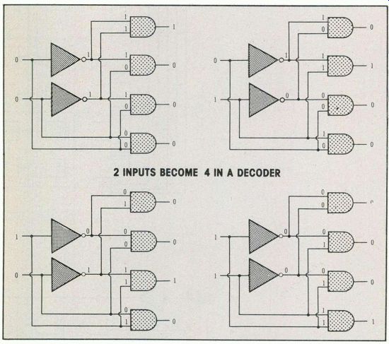
Figure 3 Two inputs to a decoder become four individual addressing lines.
(Five inputs provide 32 addressing lines in Figure 1.) The four possible inputs and outputs are Illustrated.
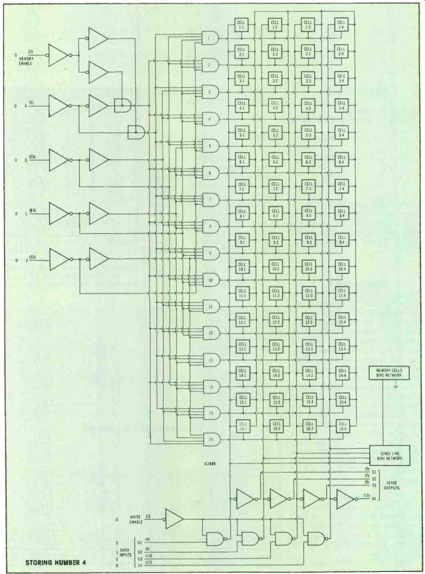
Figure 4---A 7289 RAM memory IC is shown as it stores a number 4 in row
1.
Retrieval
To retrieve a number from any row, the row-select input is set with the binary code for that row. For example, the third row stores the decimal 2 (0010 binary) of the phone number.
These settings will retrieve the phone number third digit:
Inversion One additional factor must be understood about the 7489 memory before it is used. In simpler memories, the stored data is the complement of the number entered at the data-inputs terminals. For example, if 0110 is entered, the number is stored as 1001. And the number retrieved also is a complement. Obviously, this is not desirable nor practical.
To eliminate the problem and allow storage of the correct number, inverters (NOT gates) are supplied at all of the data-input lines (D1 through D4) of the 7489. This inversion corrects the complementary numbers and allows the desired number to be stored and retrieved.
Storing the phone number Special keyboards and decoders normally are used with computers and microprocessors to store data in a memory. However, the basic principles are made more clear by manual coding, as done with the switches of Figure 5.
Each of the seven numbers is stored into the 7489 in sequence.
Remember that the 7489 is a volatile memory, and a removal of the supply voltage erases all stored numbers. If the phone number is to be kept for days or weeks, the supply voltage to the 7489 must be maintained for the entire time.
Displaying the stored number
A circuit for displaying in sequence each of the seven phone digits is shown by the block diagram of Figure 6. A binary counter is programmed to count from decimal 0 to 7 (binary 0000 to 0111), and it steps the memory through the first seven rows of cells where the phone numbers are stored. After the seventh count, the counter resets to decimal 0 and counts again up to 7, and so on.
The decoder converts the sense outputs to the code required for displaying decimal digits on the readout.
Microprocessor memory
A microprocessor can retrieve numbers from a memory that is located either inside the microprocessor IC or inside another IC. This memory can be a read-only memory (ROM) or a read/write type of random-access memory (RAM).
RAMs are not pre-programmed, but they can accept and store microprocessor information in addition to allowing the stored data to be read at any time.
These digital numbers are moved by the microprocessor along conductors called buses. Figure 7 shows the buses between a micro processor and its external memory IC. One bus is used for the address, and this corresponds to the path traveled by the select inputs.
Numbers (such as the telephone number of the experiment) are delivered to and retrieved from the memory by way of the memory-data bus.
STORING NUMBERS

Figure 5: Ten toggle switches can be used to program a phone number into
the 7489 memory IC after they are wired as shown.

Figure 6: The 7 numbers of the phone number are stored in sequence,
and this arrangement of ICs will display those numbers in proper sequence
on the LED readout.
An input device is essential for placing a number into a memory.
Usually, it converts the decimal value into its binary equivalent, and then delivers the information along an input bus. Figure 8 shows the memory bus between a microprocessor and the outside world.
When a number is retrieved from memory, it is delivered to the outside world along an output bus.
The microprocessor must send a signal to the input-output (I/O) devices to turn them on at the proper time. This prevents any receiving or delivering of data before the microprocessor is ready for it. The I/O bus is used for this purpose also.
It is common practice to reduce the number of buses by making each one serve more than a single purpose.
Bits & bytes
As explained before, a bit is a binary digit, a digital high or low.
Many of these bits must be used to instruct a microprocessor for each specific job. Types such as the 8080A and the 6800 employ 8-bit combinations (called bytes) for all instructions. For example, 00000000 informs the 8080A microprocessor that no operation is required. And 01110110 commands it to halt operations.

Figure 6: The 7 numbers of the phone number are stored in sequence,
and this arrangement of ICs will display those numbers in proper sequence
on the LED readout.
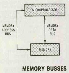
Figure 7: Busses are conductors that carry digital signals between various
sections inside an IC or between the ICs of a microprocessor system.
These busses connect a microprocessor IC with an external memory IC.
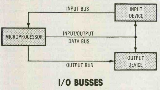
Figure 8: Other busses are those for the input and output devices that
connect a microprocessor with the outside world.
Each manufacturer supplies a code for the specific microprocessor. These codes are part of the software (instructions and pro grams) and they will be discussed in greater detail later.
These 8-bit (or one byte) codes are very unwieldy to work manually. The earliest models of computers forced the operators to feed the numbers into the processor by setting various switches. This was somewhat similar to the method shown in Figure 5.
It now is common practice to use special codes that are easier for the operators. The next article will show how to write these codes.
Also see: Link | --Flip flop memories