090 6-WAY CHANNEL SELECTOR
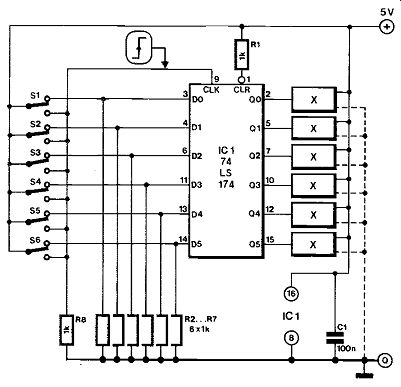
This design proves that a latching 6-way channel selector with debounced switch inputs need not always be based on the use of special integrated circuits.
--------------
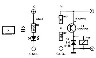
When none of the break-type SPDT push buttons is pressed, the data inputs of IC1 are held at + 5 V, while input CLK is held low via R8. When a switch is operated, the associated input of IC, goes low, while CLK goes high, so that the logic state of the Do-Ds lines is latched and transferred to outputs Q0-Q5. Each of these can drive a LED or relay based output circuit as shown.
When more than six switches are required, a 74LS174 may be added, whose clock input is connected to IC1.
Note that the LS chip may be replaced by a corresponding version from the HC or HCT family. This will reduce the current consumption from about 20 mA to 6 mA. The maximum output current sup plied by IC, is 8 mA in all cases.
091 ANALOG & DIGITAL
--------
Leafing through some electronics magazines published over the past few years, it is surprising how fast and vigorous digital techniques have come to the fore. Even audio, until recently virtually un touched, is now becoming digitalized at a rapid pace. What are the consequences of these changes to us engineers, technicians, and hobbyists alike? As long as a circuit is totally analog or totally digital, all is well. But as soon as these two techniques become mixed strange things sometimes happen. Well-known examples are analog-to-digital converters that will not give a stable reading: the last few digits do not match and it appears as if there is a certain regularity in the deviations.
Another example is an otherwise good amplifier that generates whistles in perfect rhythm with the digital clock oscillator. And so on . . .
Often, these flaws can be traced to faulty earth connections, i.e. the zero supply line, or common ground. Because of that, here are a few tips that may prevent these annoying defects.
Avoid earth loops.
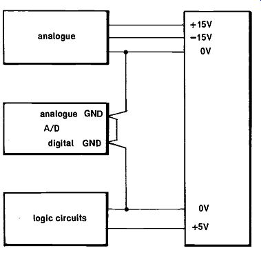
Keep the analog and the digital earths separated.
Interconnect the analog and digital earths at one point only, for instance, at the analog-to-digital converter, but NOT at the power supply.
If there are more earths, connect these to the same common point.
At high frequencies, the impedances of earth lines are not negligible: short, thick wires should, therefore, be used.
An example that gives good results is shown in the accompanying drawing. All sensitive parts of the circuits have been isolated from those parts that carry (large) earth currents. Most converters have, therefore, two earth terminals, or an earth terminal and a differential input (which is the same thing).
In audio amplifiers most of us do not dream of wiring the power supply to the output amplifier via the preamplifier. In mixed analog-digital circuits, such considerations are not so self-evident, although the principle is the same.
Note that in the accompanying drawing the system needs several electrically isolated power supplies: that is unfortunately the price often to be paid for new techniques.
092 BAND-GAP VOLTAGE REFERENCE
It is generally known that the accuracy of measurements in electronic circuits is mainly a function of the stability and reliability of the reference against which the unknown quantity is compared. Therefore, everything feasible should be done to maintain the stability of the reference, i.e., counteract the adverse effects of variations in the ambient temperature, supply voltage, and load current. The zener-diode in Fig. 1 is a usable reference device for applications where the above three parameters are not subject to appreciable variation.
The "super zener" in Fig. 2 features excellent stability and is hardly affected by variations in the supply voltage and the load current. Although the temperature coefficient of the super zener circuit can be optimized by careful dimensioning of the components, there exists a still better way for making a precision voltage reference.
The term band gap refers to the difference between two discrete energies of the outer four electrons in a semiconductor atom. Electrons in the highest energy band contribute to the conduction of the material. As the temperature is increased, some electrons gain enough thermal energy to escape from the valence (non-conductive) band, cross the band gap, and enter the conduction band, leaving the valence band unfilled. Thus, conductivity is a function of temperature.

----
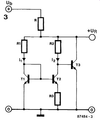
With reference to Fig. 3, the temperature coefficient of current mirror T,-T2 is compensated by that of T3. The following conditions should be met if the circuit is to function optimally:
(1): R2 10R,; (2): R3 is dimensioned such that VR-= 1.204 V; and (3): the transistors are exactly matched. The latter condition is probably best satisfied by using transistors on one and the same chip carrier, e.g. those in a transistor array such as the Type CA3083. The value of R depends on the supply voltage and the maximum output current. It should be noted that T3 carries the output current if the circuit is not loaded, so that the resulting dissipation may give rise to temperature differences on the chip. It is, therefore, recommended to permanently load the band-gap reference. The accompanying calculations prove that the output voltage of the circuit is not affected by temperature variations.
-------
Band-gap reference.
The reference voltage, UR, is obtained from UR = UBEIT3) + 12 T2.
IR.1 and R2 are dimensioned such that h = 1012, so that R3 drops I UBEIT11- UBEIT2II volts.
When the current amplification of T2 is sufficiently high, R3 carries virtually all current 12:
12 = UBE(T 1)- UBE(T2)/R3 whence UR = UBEIT 3) + (UBEIT1 I- UBE(T 2)) R2 /R 3 .
For identical transistors UBE is given for different values of IBE as UBEIT 1)- UBEIT 2 ) = k T/q10ge(11 /12 ) UBE of T3 is also expressed as UBEIT 3) = UBG( 1- T/To) + UBEO( T/To) so that UR can be written as UR = URG( 1- T/To) + UREol T/To) + R2/R3k T/qloge(11/12).
Differentiating this to the temperature domain yields dUR/d T=-UBolT 0 +UBEolT 0 + R2/133k/qloge(11/12) if R2, R3 and 11 are dimensioned such that R2/R3loge(11/12)= (URG-UsEo1T31)C where C=q/kTo which results in dUR/dT= 0 (QED).
k= Boltzman's constant (1.3805 x 10^-23 J/K).
T= absolute temperature [K].
q= charge of an electron (1.6021 x 10^-19 C).
UBG = band-gap potential (1.204 V) .
UBE0 = base-emitter voltage at T= T0.
e = the base of natural logarithms (2.71828).
093 BUZZER DRIVER
Piezoelectric resonators, also referred to as buzzers, are frequently used for providing audible signals in all sorts of electronic equipment. Buzzers are small, light, simple to use, and yet provide a loud output signal. They are either of the passive or of the active type. The former are driven by an AF signal source, while the latter feature a built-in oscillator, and re quire a direct voltage only.
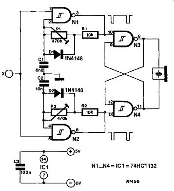
This circuit is a double AF oscillator for driving passive buzzers. It ensures a richer output sound than normally obtainable from a piezo buzzer due to the use of two oscillators, N1 and N2, whose output signal lies between 1 and 10 kHz. Gates N3-N4 form an S-R bistable which is controlled by the outputs of N1-N2, and drives the buzzer direct. The spectral composition of the output signal is fairly complex, due to the presence of both the fundamental notes and the difference and sum frequency. The timbre so obtained varies as a function of the ratio between the oscillator frequencies, which are adjustable with the aid of presets Pt-P2. Note that diodes D1-D2 reduce the duty factor of the oscillator signals to about 25%. Optimum effects are achieved when a simple ratio is set between the oscillator frequencies, e.g. 3:4. The resulting waveform is always composed of rectangular signals, but these differ in respect of their period to ensure that the buzzer produces a rather agreeable sound.
The buzzer driver is controlled by a logic level applied to point X. The quiescent current consumption is virtually negligible, while about 10 mA is drawn in the actuated state.
-----------------
094 COMBINING DIGITAL CIRCUITS
Many electronics hobbyists combine all sorts of digital circuits into works to be marveled at. however, even they sometimes have that uncertain feeling: must they all be powered by one unit or should there be more or can there be more? And in what sequence should they be switched on? Printer first, or computer first? In digital engineering, which by definition embraces computers, inputs are driven by outputs: information is being transferred. When the IC that drives has a power supply, but the receiving one has not, a current will ensue, whether the circuits are TTL or CMOS. This is an undesirable situation, although it does not normally lead to damage. But the ensuing current may be so large that the IC pro viding the current does not operate efficiently any more, because its output voltage, owing to the large current, becomes too low. Particularly bistables can become disorganized by this. It is, therefore, possible that a certain equipment does not work properly because another circuit connected to it does not have a power supply.
That situation can become really critical when several outputs of an IC are terminated in that manner. Normally, an IC can withstand a short at one of its outputs, but if that happens at several outputs, the IC will probably give up the ghost. This may happen, for instance, in the case of a Centronics interface, of which the eight data lines are normally driven by one IC.
And what happens to the IC that is provided with the current? CMOS circuits are generally well protected against this, and TTL devices normally stand up well to them also. But other types may not take so kindly to these currents.
Semiconductor manufacturers have, of course, also been confronted with these problems and have found solutions to them. Anyone designing and building his own circuits should, therefore, heed their experiences and observe the following rules.
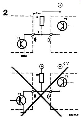
Driver ICs, whether TTL or CMOS, must have an open-collector output.
All inputs should be provided with additional resistance (pull-up resistors) to the positive supply line.
If these rules are adhered to, current can only flow from input to output (see figure 2). This does not matter, because the collector of transistor T1 can stand quite a high voltage and nothing will, therefore, go wrong. Make sure that the pull-up resistor is connected at the input side, otherwise it has no effect.
As to the question at the beginning: it does not matter which unit is switched on first, because the IC manufacturers have made sure that the input and output circuits are protected.

-------------
095 CURRENT DRIVE FOR STEPPER MOTORS
Stepper motors have either unipolar or bipolar stators. In unipolar models, each stator winding has a center tap, which enables the magnetic field to be inverted by switching from one to the other half of the winding. Bipolar types have a single stator winding, so that the direction of the current through it must be changed to attain inversion of the magnetic field. From this, it is clear that, given that the two motors are of similar size, the bipolar type will provide a larger couple than the unipolar model. There is, however, a price to be paid for this larger couple: the drive of a bipolar motor is more complex than that of a unipolar type.
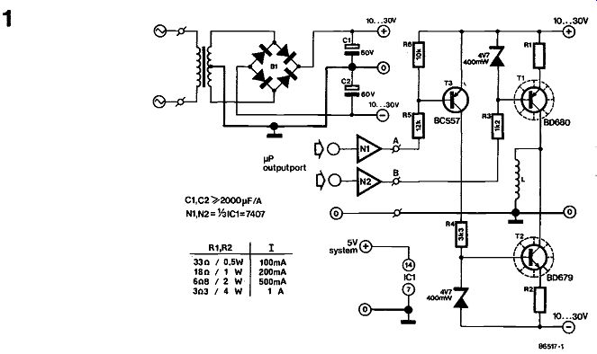
The drive for bipolar motors may, in principle, be obtained by means of a full bridge circuit. i.e. four transistors per stator winding; half bridge circuit and dual power supply, i.e. two transistors per stator winding; half bridge circuit with large output capacitor.
The last method is totally unsuitable for low stepping frequencies or stand-still. Of the other two, the half bridge is to be preferred in most cases, in spite of the requirement for a dual power supply. In this context, it should be noted that the supply need not be regulated, since constancy of current is guaranteed by a zener diode and emitter resistor, even with variable input voltage. The value of the smoothing capacitors in the power supply is deter mined by the total stator current, and is a minimum of 2000 µF/A.
Values of R1 and R2 are given for various values of stator current in the table below.
R1& R2 | Is
33 ohm ; 1W 100 mA
18 ohm;1 W 200 mA
6 ohm 8; 2 W 500 mA
3-ohm-3;4 W 1A
Current drive ensures a higher pull-in rate, i.e. permissible starting frequency, because commutation is quicker with an inductive stator winding.
The higher the supply voltage, the more effective the drive, but also, unfortunately, the dissipation in T1 and T2. In practice, a 2 x 12 V or 2 x 18 V mains transformer has proved very satisfactory. Note that freewheeling diodes have been included in the darlington circuit to give a good measure of protection against high induced voltages caused by switching.
The prototype was used in the first in stance for the control of four-phase stepper motors via an eight-bit output port of a microprocessor system. The interface used to obtain TTL levels was a Type 7407 which has 30 V open-collector outputs. The control instructions may be generated as trot instructions may be generated as follows:
Phase 1 2 3 4
Bit 7 6 5 4 3 2 1 0
Output byte 1 0 1 0 1 0 1 0 initial position
Auxiliary byte 0 0 0 0 0 0 1 1 XOR with output byte
New OtP byte 1 0 1 0 1 0 0 1 made one step
Rotate aux. byte twice*
0 0 0 0 1 1 0 0 preset for next step
*Direction of turning determines rotational direction of motor.
--------------
If the stepper motor is required to be used on its own, this may be done with the aid of commercially available control ICs such as the SAA1027 or the TEA1012. The latter is dealt with in Circuit 119 (p. 146) and may be connected as shown in Fig. 2.
096 DC OPERATED 50 HZ TIME-BASE
Many clocks, both of the digital and the analog type, make use of a 50 Hz timebase signal which is usually derived from the mains. In order that these clocks may also work in places where there is no mains supply available, as in cars, on boats, or, say, on a camping site, this one-chip circuit provides an accurate 50 Hz square wave output signal, while being fed off any DC supply voltage between 6 and 15 V (battery, solar cell array, etc.). Current consumption of the circuit is only 3 mA (max.).
The Type SAF0300 by ITT Semiconductors merely requires a crystal to perform the above task, while also offering the possibility to adjust the exact output frequency by means of seven active low bits as listed in the pin assignment table.
If a 64 Hz output frequency is desired rather than 50 Hz, the crystal may be replaced with a 4.194812 MHz type.
Finally, the 50 (64) Hz output pulse has a voltage swing of nearly the IC supply voltage, and a duty factor of 0.5.

---------
1 Output 1 (50Hz) 2 Adjustment pin 122 ppm 3 Adjustment pin 61 ppm 4 Adjustment pin 30.5 ppm 5 Adjustment pin 15 ppm 6 Adjustment pin 7.6 ppm 7 Adjustment pin 3.8 ppm 8 Adjustment pin 1.9 ppm 9 Test pin M (ix/4) 10 Cristal connection 11 Cristal connection 12 Bridge output 13 Bridge output 14 Ground, 0 15 Leave vacant! 16 Supply voltage
097 DECOUPLING IN LOGIC CIRCUITS

-------------
Failing to heed the importance of adequately decoupled supply rails is one of the most serious mistakes a constructor of digital circuits can make.
Two important facts necessitate a reappraisal of the effectiveness of decoupling: the introduction of the fast HC and HCT series of CMOS chips, and the general availability of ever larger dynamic RAM (DRAM) devices. The 41256 256Kbit DRAM and 6264 CMOS SRAM, for instance, have become commonly used integrated circuits, available at relatively low cost. The fast spreading use of the new CMOS series of logic circuits has created the widely heard misunderstanding that these devices can be used without paying the least attention to decoupling of the supply lines. However, a reduced current consumption relative to TTL devices is by no means a carte blanche for designers to skimp on decoupling provisions, as will be seen below.
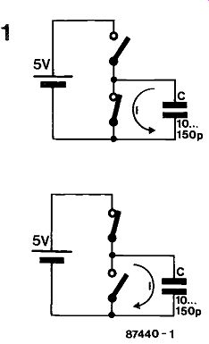
Why does a logic circuit draw current? The current consumption of TTL chips goes mainly on account of indispensable, internal, resistors. CMOS structures are complementary, and theoretically consume no current at all in the static mode. As soon as any kind of switching is to be done, both by TTL and CMOS circuits, the charge of the capacitance at the output must be reversed as illustrated in Fig. 1. The switch currents internal to the IC are only a fraction of those required for the load capacitance, and can, therefore, be disregarded, except in the case of counters.
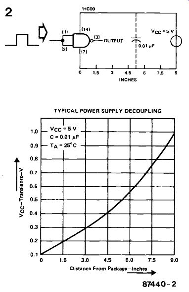
TTL and CMOS circuits thus consume an equal peak current during switch operations. Decoupling capacitors are fitted direct to the IC supply terminals to prevent the instantaneous supply voltage from briefly dropping to an unacceptable level when the switching takes place. The graph in Fig. 2 is reproduced from a Texas Instruments data-book, and shows the correlation between the capacitor-to-package distance and the peak amplitude of the spikes on the supply line to a typical HCMOS gate. This shows beyond doubt that decoupling capacitors must be fitted as close as possible to the IC supply terminals, to rule out the stray inductance of supply tracks on the PCB, however neatly these may run in parallel. Often, tuned circuits are designed with long supply tracks and a wrongly placed decoupling capacitor. Any spike is then subject to ringing effects, which further deteriorate the operation of the logic circuit in question. Not surprisingly, Mullard recommend a multi-path supply track when it is impossible to fit the decoupling capacitor close to the IC. This solution is called a grid structure, and is definitely preferable to creating relatively wide, single tracks--see Fig. 3.
The value of the decoupling capacitor must be based on the foreseeable number of IC outputs that are simultaneously active. A conventional starting point is 20 to 100 nanofarad for every three ICs.
Further reflection on this theme leads to the conclusion that the supply for a 256Kbit DRAM is far more difficult to decouple than that for, say, a 16 Kbit DRAM. Fortunately, the problems are not as serious as one would expect. In practice, the size of the chip carrier, and hence the parasitic capacitance, is constantly reduced by the manufacturers, whose foremost aim is to ensure optimum response of the device at high operating frequencies. Certain DRAM manufacturers recommend the use of 330n decoupling capacitors (see Fig. 4), but in practice no problems evolved from the use of the standard value of 100n.
--------------
098 DE-GLITCHER
Extremely short, unwanted, pulses with a period in the nanosecond range are often referred to as glitches, and occur in most, if not all, digital circuits.
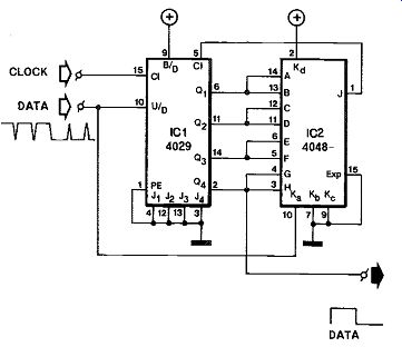
Whilst the circuit in question can be designed and built with due attention paid to effective suppression of glitches, it is not always possible to foresee the effects of external noise on, for instance, a clock signal. The filter presented here effectively rules out the presence of glitches in a serial data link.
Assuming that counter IC1 is at state zero, and that the data input is logic high, IC2 is configured as an AND gate. Output Q4 of IC1, and hence the output of the deglitcher, goes high after 8 clock pulses. A short negative pulse at the data input merely results in a few more clock pulses being required before Q4 is activated. After another 8 clock pulses, the counter state is 15. This causes the C1 (CARRY IN) input of IC1 to be driven high, so that the clock signal remains blocked as long as the data input is logic high. When it goes low, IC2 is configured as a NOR gate, enabling the clock transitions to be counted down in IC1. Output Q4 goes low again after 8 clock pulses, and the counter is blocked after another 8 pulses. Therefore, the filtered output data is delayed by 8 clock periods, but this is insignificant in the proposed application.
The data frequency fd depends on the clock frequency, f_cl:
f[D] = f[CL]/16
The maximum usable clock frequency is about 8 MHz. The current consumption of this circuit is less than 1 mA.
------------
099 DESIGNING A LOW NOISE AMPLIFIER
To design a low noise amplifier, it does not suffice to choose a low noise opamp, because the components associated with the opamp, particularly resistors, are themselves sources of noise. The noise in a resistor, which is caused by random movement of electrons, increases by the square root of the increase in resistance.
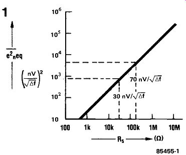
Figure 1 shows a very convenient characteristic for determining optimum values of input resistance.
The y-axis gives the square of the sum total of noise voltage produced in a circuit (in nV over the band width considered), while the x-axis gives the value of the source resistance.
For instance, a noisy opamp like the 741, which produces some 70 nV of noise over its bandwidth, can cope with an input impedance of some 200 k (higher values would cause the input impedance to generate more noise than the opamp!). On the other hand, the less noisy TCA 520, which generates about 30 nV of noise over its bandwidth, should have an input impedance not greater than about 50 k.
-----------
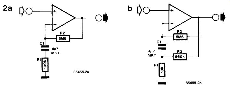
It is not always convenient to use such relatively low values of resistance. For example, the audio amplifier in figure 2a is intended to operate down to 0.3 Hz; because of that, the time constant, r= RC, must be fairly long. The input (= source) impedance of the opamp is determined primarily by Ri. Lower values of this resistor would require a higher value of C1 and this is not acceptable on cost grounds. The solution to this problem is shown in figure 2b, where both the DC and AC amplification are the same as in la, but because I?, is 10 times as small, its noise voltage is reduced by 1/10.
Sources: Figure 1: intuitive IC opamps (T M Frederiksen- National Semiconductor) Figure 2: technical note 068 (Philips)
-----------
100 DISPLAY INTENSITY CONTROL
This is a light dependent voltage source that regulates the supply to 7-segment displays in accordance with the intensity of ambient light. The regulating action is positive, i.e., a higher ambient light intensity results in the circuit raising the supply voltage to the displays.
Phototransistor T1 does not conduct when it detects darkness, and the base of T2 is therefore grounded via R2 and Pt This causes the voltage at the emitter of this pnp darlington transistor to be about 1.2 V.
The voltage across R5 is the reference potential, 1.25 V of the Type LM3I7 regulator, so that I_Rs is about 5.7 mA, and the output voltage, Uo, of the circuit is:
U0 =1.2 + [5.7 x 10^-3(R5+ R3)] =1.2+1.82 = 3 volt
… when T1 detects darkness.
When it detects a relatively high light intensity, the base and emitter voltage of T2 increase. When the base voltage of T2 exceeds 2.7 V, R4 limits the emitter voltage to 3.9 V due to the constant current of 5.7 mA. T2 no longer conducts and the output voltage of the circuit is 5.7 V, because the total resistance between the regulator output and ground is R5 + R3 + R4 =1,000 ohm, and the current through it is still 5.7 mA.
The sensitivity of the regulator is adjustable with Pt The maximum output current is of the order of 700 mA when IC1 is adequately cooled. The input voltage range of the circuit is 8 to 15 V.

--------
101 DUTY FACTOR ANALYZER
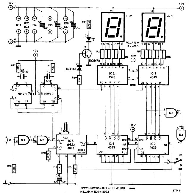
Applications of this duty factor meter include adjusting and setting up ignition systems, switch mode power supplies, PD modulators, and sensor signal converters. The circuit itself requires no adjustment, and has a duty factor resolution of 1%, or 1° in terms of the dwell angle. The duty factor range is 1% to 99% in the frequency range from 1.5 Hz to 10 kHz. The analyzer is fed from 12V and consumes only 50 mA, so that it can be readily used in a car.
--------------
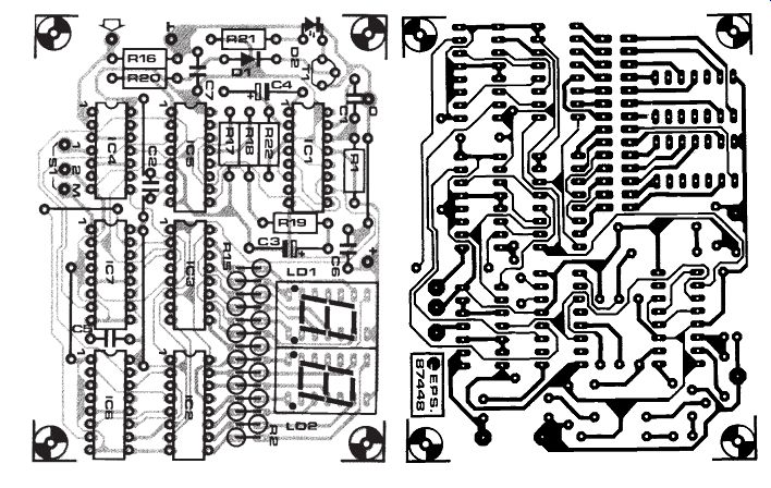
Parts list:
Resistors ( ± 5%):
R1 = 10K
Ris W
470R
R16 100K
Rtr R R A 3 1MS
Capacitors:
- 1 2OP
C Ca is C4 y: 6V
C 0, 1 OOr C 220n
Semiconductors:
D1- 1N4
- LED green T 8C547B C 4526 ICa;IO 4543 C
'C 4048 CEIC 4029
LD.;LD2 – common-anode type e.g. 7851 or 7766.
M S. = SPDT switch.
PCB Type 87448
-----------
The measuring principle is straightforward. A PLL, ICS, is used to multiply the input signal by a factor 100 and to clock counter IC6-IC7, whose BCD outputs are applied to display' drivers IC2-IC3. The carry output of IC7 is fed back to the phase comparator in the PLL. The counter state is only latched and displayed upon the falling edge of the input signal.
Since the counter always counts up to 100 (leading edge of the input signal); the output state that exists upon detecting the trailing edge corresponds to the percentage of the pulse duration in relation to the period. Example: assuming that the duty factor of the input signal is 60%, the counter is started at state 00 on the leading edge of the input signal, and is at state 60 when the trailing edge commences, so that '60' is latched and displayed. The latch pulse is generated with the aid of n IC and liming parts R'-C while RnC4 ensure that the display does not flicker when the input frequency is equal or close to the sample frequency. Each display value is S retained br about 0.5s. Switch S1 selects between duty factor (position 0-99%) and dwell angle readings 0-90. The latter scale s obtained by programming a divide factor and hence a PLL multiplication factor, of 90 with the aid of NAND gates N3-N4.
The input impedance of the duty factor analyzer is 100 k-ohm. Input signals should be at least 8 Vpp a suitable preamp set up with a switching transistor ' be added to increase the sensitivity.
102 ELECTRONIC ROTARY SWITCH
Sooner or later, most types of frequently used multi-way rotary switches develop contact resistance in stability or other malfunctions, either caused by internal oxidation or wear and tear of the rotary mechanism. Broadly speaking, the same goes for multi-contact relays. It is, therefore, hardly surprising to encounter the electronic, free-of-wear equivalents of the above devices; n-way electronic switches and solid-state relays are at present available in a wide variety of contact arrangements.
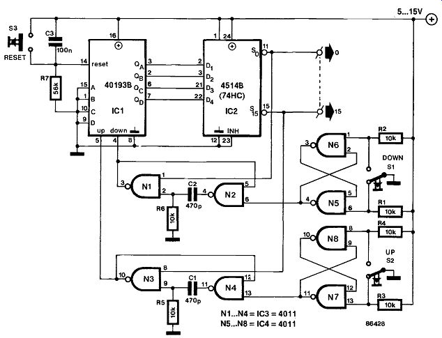
The circuit diagram shows the electronic counter part of a 16-way rotary switch whose pole is connected to earth. Two push buttons have been provided to enable the switch to be "turned" clockwise (up) or anticlockwise (down).
Debouncing bistables N5-N6 and N7-N8 supply a stable low logic level to monostables N1-N2 and N3-N4 respectively in order that these can output approximately 3.5 us long pulses to the relevant input of up/down counter IC1. The rising edges of the up/down pulse(s) cause this IC to generate the corresponding binary code at its QA. QD Outputs, which are connected direct to the D1 ... D4 in puts of latching 4-to-16 decoder IC2 which, in turn, activates the next lower or higher output S0 ... S15 if the relevant control button was activated. Provision has been made to "stop" the switch if this reaches its first or sixteenth position, which conditions cause the down or up monostable respectively to be disabled. Other switch configurations may be defined by using the correct active-low outputs to block gates N2 and N4 when the desired stop positions are reached.
Finally, push button S3 resets the counter IC and consequently causes IC2 to activate its So output, which is also the default switch position at power-on.
---------------
103 FAST OPTO-COUPLER
The opto-coupler in the normal common emitter circuit at the output of a phototransistor is in variably too slow for use in data communication.
Its great advantage remains, of course, the excellent isolation between transmitter and receiver.
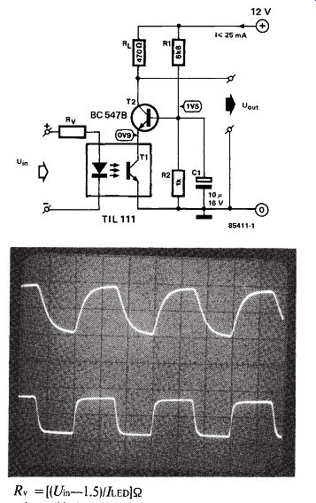
To retain the advantage, the phototransistor has been integrated into a cascode circuit, as shown in figure 1. The photograph illustrates data transfer in a conventional circuit (top) and in the cascode circuit- the fast opto-coupler- (bottom) at a frequency of about 30 kHz.
The cascode circuit's faster operation is due to the transistor's internal Miller capacitance being of no consequence as the collector voltage remains constant. The result is a faster transistor.
The base of T2 is biased at about 1.5 V by voltage divider R1/R2. Capacitor C1 ensures that, even with rapid fluctuations in current, this voltage remains stable. If you consider 12 as an emitter follower, it is clear that the collector of T1 is always provided with a constant (direct) voltage, and this causes the Miller (base-to-collector) capacitance to be inactive.
A disadvantage of the fast opto-coupler is that its output signal does not go down to 0 V but at best to 1V. TTL devices like this just as little as they do a supply voltage of 12 V. Basically, the circuit can operate from 5 V, provided R, is altered suitably, but it is better to use CMOS devices.
---------
Take care during experimenting not to exceed the maximum LED current (in the TIL 111) of 100 mA (this is the reason for dropping resistor Rv). The value of Rv is calculated from:
Rv =[(Uln-1.5)//LED] ohm
… where U in is in volts and /LED in amperes.
104 FAST OPTO-ISOLATOR
When a computer drives external equipment, it is often required that the earths between them are electrically isolated from one another. The simplest way of effecting this is by an isolating transformer.
When, however, the system works at high frequencies, it is much better to use an opto-isolator as proposed here because that is capable of following the fast data transfer.
The opto-isolator is driven via a TTL gate. The transistor in the opto-isolator drives comparator IC,.
The trigger threshold of this device is set with Pt. Low-pass filter R2-C1 prevents spurious triggering of the comparator by noise pulses.

105 HC-BASED OSCILLATORS
Two inverters, one resistor and one capacitor are all that is required to make a HC(T)-based oscillator that gives reliable operation up to about 10 MHz.
This sort of circuit is well-known, and appears in Fig. 1a.
The use of two HC inverters gives fairly good symmetry of the rectangular output signal. In the same circuit, HCT inverters give a duty factor of about 25%, rather than about 50%, since the toggle point of an HC and an HCT inverter is 'AV., and slightly less than 2 V, respectively.
When the supply voltage for the oscillator is switched on, C initially has no charge, and the output of N1 and N2 are at the same logic level. Capacitor C is then charged via R, until it has acquired a charge voltage that corresponds to the toggle voltage, Us, of N1. Assuming the output of N2 initially to be logic low, the waveform of the signal at the in put of Ni is essentially as shown in Fig. 2. When C is charged up to level 1 , the output of Ni toggles, and so does that of N2. This causes the voltage at the input of N1 to rise, via C, to about 1.5Vcc, so that C is reverse charged to level 3 . From there on, the amplitude changes in a mirror-inverted way to reach the initial state again (level 5 is identical to 1 ), and the circuit oscillates. In practice, the curve in Fig. 2 is slightly flatter, because the peaks at levels 2 and 4 are clamped to + 5 V and 0 V by the protective circuits internal to the inverters.
If the oscillator is to operate above 10 MHz, the resistor is replaced with a small inductor, as shown in Fig. lb.
The output frequency of the circuit in Fig. 1a is given as about 1/1.8 RC, and can be made variable by connecting a 100K preset in series with R. The solution adopted for the oscillator in Fig. lb is even simpler: C is a 50 pF trimmer capacitor.

---------
106 HCMOS VCO
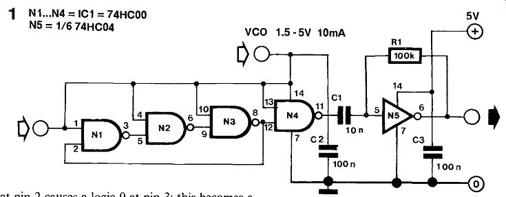
Crafty designers are forever trying to use ICs for applications they were never intended for. In this circuit a member of the newish HCMOS family is used as a voltage-controlled oscillator (VCO). This is achieved by using the characteristic of the HCMOS family of operating from a 2 to 6 volt supply. However, at 6 V these ICs are faster than at 2 V.
-----------
In the present circuit, a "supply voltage" variable between 1.5 and 5 V is used as the input signal of the oscillator, which consists of three cascaded NAND gates. The VCO operates as follows: a logic 1 at pin 2 causes a logic 0 at pin 3; this becomes a 1 at pin 6, and a 0 at pin 8. Pin 8 is, however, connected to pin 2, which, therefore, is no longer 1 but becomes 0. This 0, because of the delay times of the gates, appears a little later at pin 2 as a logic 1. And so on: the oscillator works! Gate N4 functions as a buffer for the oscillator output.
Since the peak output voltage cannot be greater than the supply voltage, i.e. the input voltage to the oscillator, its level must be adapted to those at the remainder of the circuit, which normally will be 5 V. This is ensured by inverter Ns, which is powered by a genuine 5 V supply. Because of feedback resistor 121, the inverter is arranged as a linear amplifier. It is, therefore, sufficiently sensitive to amplify positive signals between 2 and 5 V adequately.
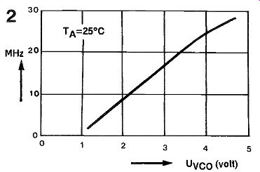
The characteristic in Fig. 2 shows that the VCO is reasonably linear. Other output frequencies are not possible with the circuit of Fig. 1, unless the number of gates in the oscillator proper is extended by an even number of identical gates, which increases the total delay times, so that the frequency is lowered. It is also possible to add dividers to the output circuit.
107 HCU/HCT-BASED OSCILLATOR
When frequency stability is not of prime importance, a simple, yet reliable, digital clock oscillator can be made with the aid of relatively few components.
High-speed CMOS (HCU/HCT) inverters or gates with an inverter function are eminently suitable to make such oscillators, thanks to their low power consumption, good output signal definition and extensive frequency range.
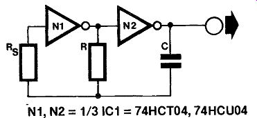
The circuit as shown uses two inverters in a 74HCT04 or 74HCU04. The basic design equations are for HCU: f =1/T; T=2.2RC; 3V<Vcc<6V;
L =13 mA
for HCT: f =1/T; T=2.4RC; 4.5V<Vcc<5.5V;
lc =2.25 mA Rs 2R; 1K-OHM.5..R.s.1M52; nF.
-N1, N2 = 1/3 IC1 = 74HCT04, 74HCU04 87437
With Rs and R calculated for a given frequency and value of C, both resistors can be realized as presets to enable precise setting of the output frequency and the duty factor. Do not forget, however, to fit small series resistors in series with the presets, in observance of the minimum values for R and R5 as given in the design equations. The values quoted for Ic are only valid if the inputs of the remaining gates are grounded.
Source: Philips CMOS Designers Guide, January 1986, p. 105 ff.
108 HEART BEAT MONITOR
The proposed circuit is based on the fact that the degree of translucence of parts of a mammal's body depends, among others, on the flow of blood.
Because the blood supply pulsates at the frequency of the heartbeat, this may be monitored in a simple way without the need for an electrical connection between the mammal and the measuring equipment.
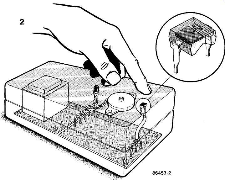
In the proposed circuit, the flow of blood through a finger is monitored. To obviate errors caused by the position of the finger, the receiver diode is included in a loop.
The positive input (terminal 3) of IC1 is held at about 2.5 V. The gain of the device is determined by the ratio R5:R4. Network R6-D2 ensures that the circuit stabilizes rapidly. The amplified signal is rectified by IC2. Time constants R8-C4 and R2-C4 are chosen such that the potential at pin 2 of IC2 has a sawtooth shape. The CA3130 in the IC3 position functions as a trigger. The output signal may, for in stance, be applied to the input port of a computer.
If a computer is not available or deemed necessary, the beat is made audible by a piezo-electric buzzer operated by gates N1 and N2.
Circuit IC5 provides a WAIT indication that shows when the circuit has stabilized and is ready for use.
The program is compiled as follows: wait for a trailing edge, then count until the next trailing edge appears. The count is converted into a number per minute, and this is displayed on the monitor screen.
However, the heart beat is not constant, which is quite clear from listening to the buzzer or observing the monitor screen. It is, therefore, advisable to calculate an average over, say, sixty seconds. It is then possible to display the instantaneous value, the average value over 60 seconds, and the trend (rise or fall).


-----
Once the program is known to work satisfactorily, it becomes interesting to display the actual signal on the screen. If the computer used has an analog-to-digital converter, the output signal of IC, may be used for the display.
------------
109 HEAT SINK MONITOR
In almost any equipment in which a reasonable amount of energy is consumed, there is bound to be at least one heat sink that enables power semiconductors to get rid of their excess heat. The rating of a heat sink is normally determined on the basis of the maximum allowable temperature of the silicon chip: a rather haphazard method.
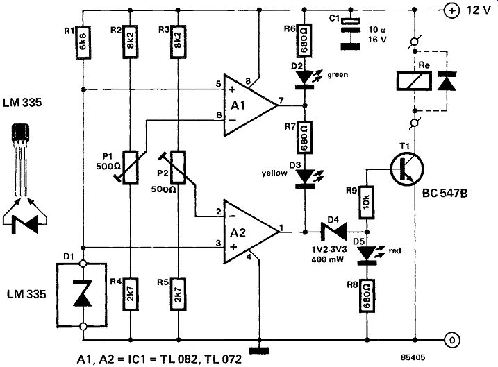
The heat sink monitor described here constantly monitors the temperature of the heat sink. When that temperature stays below 50 ... 60°C, the green LED lights; between those temperatures and 70 ... 80°C, the yellow (orange) LED lights; and above 70 ... 80°C, the red LED lights. There is also the possibility of providing a relay with which, for instance, the load can be disconnected.
The circuit is, in essence, a window comparator, in which sensor D1 provides a control voltage that rises 10 mV per degree Celsius. If the sensor voltage is lower than the voltage at the wipers of Pi and PA the outputs of opamps A1 and A2 are low, and D2 lights. When the voltage across D1 lies above that at the wiper of Pi, but below that at the wiper of P4 the output of A1 is high, so that D2 goes out and D3 lights. When the sensor voltage rises above that at the wiper of P2 also, the output of both opamps is high: only Ds then lights and transistor T1 is switched on. Zener D4 ensures that D5 lights brightly and that T1 conducts hard.
To calibrate the unit, place the sensor, together with a calibrated thermometer, in a tray of water, which is then heated. Set Pl to minimum and P2 to maximum resistance. Set the cross over from green to yellow (orange) between 50 and 60 degrees Celsius with P1 Next, set the cross over from yellow (orange) to red between 70 and 80 degrees Celsius with P2 The sensor can then be fitted permanently onto the heat sink.
----------
110 LOGIC FAMILIES
The introduction of new, faster, CMOS techniques has given rise to a considerable increase in the number of available logic families. Understandably, this may cause confusion on the part of designers and users of logic circuits. Up until a few years, 3 families were commonly known: the CMOS 4xxx series; the TTL 74xx series; and the 74LSxx low-power Schottky series. TTL and LS chips are mutually inter-changable, but TTL consumes considerably more current at the same switching speed.
The 4xxx series is about 10 times slower than the TTL family, but is more economic as regards current consumption. In many cases, TTL chips are no longer considered suitable for new design.
The new HC and HCT CMOS families are just as fast as TTL and LSTTL, and have a greatly reduced current consumption. HCT chips can work in LS based circuits, provided they are not driven from TTL or LS. This is because of the differently defined switching levels. It is, however, possible to use HCT for driving HC. With this in mind, it is possible to replace the LS family by the HC family. This is preferable since the HC family offers the highest noise immunity.
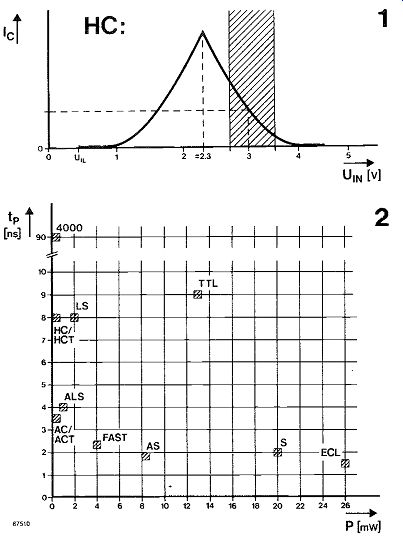
Figure 1 shows the current consumption of a HCMOS gate as a function of the input voltage.
The shaded area represents the (logic high) output voltage of an LS chip. From this, two conclusions can be drawn. Firstly, the noise margin is very narrow: the HC gate sees 2.7 V as a logic high level already. Secondly, the current consumption of the gate is a few mA higher than necessary. Although usable in practice, driving HC with LS is, therefore, not recommended.
Another new logic family was recently introduced: FACT (Fairchild Advanced CMOS Technology), also referred to as ACL (Advanced CMOS Logic) by other chip manufacturers. There are 2 versions: AC and ACT. ACT, like HCT, is fully LS compatible, while AC gives the same drive problems as HC.
Both series are typically 2 to 3 times as fast as LS or HC.
Figure 2 shows the correlation between the propagation delay, tp, and the power consumption, P, of various logic families. It will be noted that the modern CMOS families are almost as fast as the ECL series, hitherto renowned for its unbeatable speed. It is expected, therefore, that a CMOS equivalent will soon be available for ECL, and that ECL will gradually become obsolete.
Replacing bipolar chips in existing circuits with CMOS types is not very useful if relatively high frequencies are involved. Finally, a rule of thumb for working with chips of different families in a single circuit: HCT can replace LS, unless driven by LS.
For further reading:
RCA CMOS Databook Fairchild FACT Logic Data Book
-----------
111 LOW VOLTAGE DROP REGULATORS
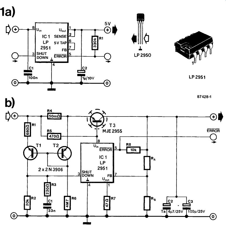
The fast spreading incorporation of CMOS, HC and HCT chips has created a need for voltage regulators with a very low internal drop to enable powering CMOS-based equipment from a set of batteries delivering 6 V. The recently introduced Types LP2951 and LP2950 from National Semiconductor are micropower voltage regulators with a variable output voltage of 1.24-29 V and a fixed output voltage of 5 V, respectively. The former features an internal voltage divider with a 5 V tap bonded out to a pin, a logic compatible shutdown input, and an open-collector ERROR output which warns of a low output voltage, often due to an insufficient battery voltage at the input. The ERROR output is extremely useful for an early warning system that arranges for a microprocessor to be reset properly before the supply voltage falls to a level that would upset the operation of the system it controls.
The voltage drop across the LP2951 is only 0.4 V at a load current of 100 mA, so a 6 V battery pack can be used to power a 5 V circuit. The quiescent current drain of the regulator is about 12 mA at an output current of 100 mA. This is fairly high as compared with a conventional regulator from the 78XX family, and mainly due to the internal series regulator transistor being driven into saturation, which causes it to have a relatively low current amplification factor (the base current flows into the ground return line, instead of into the output load, as with the typical 78XX regulator).
------------
The application circuit shown in Fig. 1a should be fed from an input voltage of more than 5.4 V, while its maximum output current is 100 mA. Note that both the LP2950 and LP2951 feature internal current and thermal limiting circuits. The decoupling capacitor at the output of the regulator should be a good quality tantalum type, fitted as close as possible to pins 1 and 4. At relatively low output currents, less capacitance is required in this location.
For currents below 10 mA, 0.33 uF is satisfactory, while the minimum value is 0.1 1.4F for currents below 1 mA. These values apply to an output voltage of 5 V; for lower voltages, more output capacitance is needed.
The circuit in Fig. lb is a 2 A low dropout regulator based on the LP2951. The output voltage is calculated from Vo= (1 + RA/RB)1.23V where 1.23 stands for the voltage at the feedback in put, pin 7. For an output of 5 V, RA and Rs may be omitted, and the feedback input pin 7 can be connected direct to the 5 V tap (pin 6) output. The sense input, pin 2, is then connected to the V0 rail.
In this application, Vin must be at least 0.5 V higher than V0.
National Semiconductor applications.
112 MAINS ZERO-CROSSING DETECTOR
Both safe and remarkably simple to construct, this circuit detects the zero crossing moments of the mains voltage, in order to provide other circuitry with timing information about the correct instant for switching mains-connected loads; in other words, when the least possible switching dissipation is involved, and, therefore, least interference is induced on the mains lines.
The proposed circuit operates direct off the mains, while comprising no more than two opto-couplers and two resistors. It is seen that photodiodes D1 and D2 are connected in antiparallel while being fed with the mains voltage via a resistor, which limits the current through the relevant diode to about 2 mA as it conducts (i.e. lights) during the negative or the positive half wave (D2 or D1 respectively) of the mains sinewave; in either case, the circuit output voltage is low, since the associated phototransistor conducts and draws current from:
+Ub via Rz.
However, at the moment of zero crossing, neither one of the diodes conducts, and the voltage at the circuit output rises to near + Ub level, whence the 100 Hz pulse train.
The value of R2 may be adapted to suit the level of + Ub and the manufacturer-specified typical collector current through the phototransistor. For the Type TIL111, the current should not exceed about 50 mA. The type of optocoupler used in the circuit should not be very critical, but the value of R1 had best be left at the indicated 100 k so as not to run into excessive diode dissipation.

------------
113 OPAMP-BASED CURRENT SOURCE
A current source based on an operational amplifier alone is likely to be less known than the combi nation of an opamp and a transistor. This latter circuit can, however, only supply a unidirectional current, and must incorporate a stable reference capable of sourcing the required current. The circuit proposed here is different from the usual design for a current source, because it has a real differential, high impedance, input.
In spite of the small number of components in this circuit, its operation may not be apparent at a glance. An example calculation example may help to clarify how the current source works.
Assuming that 10 V is applied to input 2, and 4.5 V to the output, the voltage drop across R2 is 0.5 V, and that across R4 is 5V. It will be recalled that the output voltage of a current source is determined by the value of the external resistance. The current passed through this gives rise to a voltage drop that need not be constant.
When input 1 is 1 V more positive than input 2, the following circuit potentials can be deduced:
The + input of the opamp is at + 9.5 V, because R2 drops 0.5 V. The operational amplifier starts regulating its output voltage until it detects equal voltages at its + and- input. The voltage drop across R1 thus rises from 0.5 V to 1.5 V, while that across R3 is increased tenfold, i.e., amounts to 15 V.
The output voltage of the opamp is then 11-1.5 15 =-5.5 V. When it is recalled that the output voltage of the circuit is + 4.5 V, the drop across R5 amounts to 4.5-1-5.5) =10 V. Since Rs =
100R, the current is 10/100=100 mA.
It is also possible to establish the output current of the circuit as follows. The amplification is 10 (R3/121), and the output voltage is available across R5, which therefore carries a current of U. x 10/100, or U./10.

This circuit is probably best operated on the basis of power opamps, such as the Types L149 and L150 from SGS-Ates, which can handle currents of several amperes. The Type OP50 stated in the circuit diagram is suitable for relatively low output currents ( Linz 50 mA), and features excellent stability and precision. Its manufacturer, PMI, states that this application of the opamp is capable of handling resistive, capacitive or inductive loads equally well.
Source: PMI, Analog Applications
Seminar 1986:
Current transmitter (Howland current pump).
114 PIERCE OSCILLATOR
In addition to the description elsewhere in this chapter of HC and HCT based R-C/L-C oscillators for use up to 20 MHz, this design brief concentrates on quartz-controlled oscillators which find applications in digital equipment and microprocessor systems. Such oscillators can only be made with HCU gates, because HC and HCT ones have buffered outputs that make them unsuitable for use as analog amplifiers.
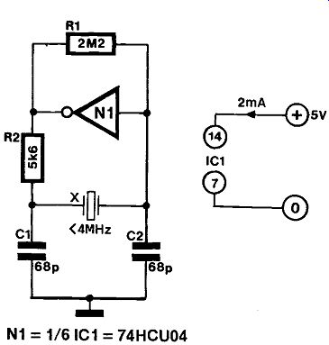
The circuit diagram shows a Pierce oscillator set up around a single gate in a Type 74HCU04 package.
The inverter functions as an inverting amplifier with a phase shift of 180°. The circuit can be modified into a Collpits oscillator by replacing the quartz crystal with an inductor. It should be noted, however, that the use of a quartz crystal is more appropriate because it ensures minimum current consumption and adequate suppression of the third harmonic frequency. Finally, R2 must be replaced with a 33p capacitor if the oscillator is operated above 4 MHz.
-------------
N1 = 1/6
IC1 = 74HCU04
87407
115 POWER SUPPLY SEQUENCING FOR OPAMPS
Most designers know that many problems may arise between the paper design and the practical realization of that design. We are, of course, no exception, and one incident that we experienced recently illustrates a problem that is of interest to pass on.
Measurements were being carried out on a circuit that contained some type NE 5532 opamps which were powered from a ± 12 V symmetrical supply.
When the circuit was switched on, it did not function correctly. Measuring the supply lines revealed that the positive supply was -0.6 V instead of + 12 V. When the +12 V line only was switched off and immediately on again, the malfunction disappeared. Switching off the mains and immediately on again made the defect reappear. Using new opamps made no difference.
After some research in relevant literature, it appeared that on switching symmetrical power sup plies temporary polarity reversal may occur.
Because of the complex internal structure of integrated circuits, it may happen that this polarity reversal causes parasitic components on the chip to be actuated which places the IC in a stable but malfunctioning state.
------------
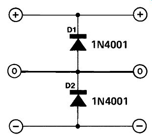
The book we consulted, Intuitive IC Opamps, suggests that the malfunction we experienced was probably caused by a parasitic thyristor being triggered owing to the negative supply not rising fast enough. The remedy proposed was to connect two diodes across the supply lines as shown in the ac companying figure: these diodes effectively prevent polarity reversal.
This simple remedy certainly cured the malfunction in our circuit and is probably the simplest protection circuit in this issue.
Literature:
Intuitive IC Opamps by Thomas M Frederiksen, National Semiconductor Corporation
116 PRECISION CRYSTAL OSCILLATOR
When designing crystal oscillators, it is good practice to ensure minimum capacitance of the active element(s), since any parasitic loading of the crystal is bound to derate the overall stability to some extent. This forms the underlying principle of the design described here, albeit that good results are also obtainable when an additional load capacitance is connected in parallel with the existing parasitic capacitance, but only if the former is known to possess a low loss factor and a low temperature coefficient, i.e., if it is a very high quality capacitor (and possibly difficult to obtain).
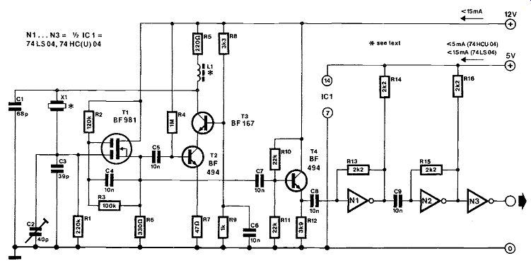
The oscillator proposed here is a Pierce type, in which the crystal operates in parallel mode. The in put is formed by a bootstrapped source follower, DG MOSFET T,, which has a parasitic capacitance of only I pF. RF transistors T2-T3 are set up as a cascode amplifier. A type BF494 transistor is used in the T2 position because of its low B-E capacitance (0.15 pF typ.), which ensures a low output capacitance. The oscillator signal is taken from the source of Ti, buffered in Ta, and made logic compatible with the aid of gates Ni-N3. The optimum inductance of L1 is approximated with L1 =1/f, where the inductance and frequency are in milli-henries and megahertz respectively.
Example:
for f =10 MHz, L1 works out at 100 µH. Trimmer C2 serves to accurately tune the crystal oscillator to the required frequency. The oscillator works well up to about 20 MHz.
Finally, although the dissipation of the crystal is not expected to give rise to instability, it is still a good idea to keep an eye on its output amplitude so as to preclude the protective diodes in T, being activated and causing unacceptable instability. If required, R7 is altered until the signal amplitude at the emitter of T4 is less than 1 Vpp.
------------------
117 SMART LED SELECTOR

-----------
A = green or yellow
B = identical colored LEDs
In this tiny circuit, for use in, for instance, a two-lights model railway signal, one of two LEDs may be selected with either a single pole switch or a series transistor, as shown in the circuit diagrams.
Note that the LEDs are fed via a common current limiter resistor, while a switch is connected in series with one of the LEDs.
Why do not both light simultaneously when the switch is closed? Because, apart from their colors, the two LEDs also differ as regards their forward voltage drop; when connected in parallel, therefore, the LED having the lower voltage drop should be fitted with the series switch; this arrangement causes the high voltage drop LED to light when the switch is open and to go out when the switch is closed, at which moment the other LED takes over.
Two of the accompanying four small circuits show the use of a series switching transistor rather than a real switch, but the difference hardly requires further detailing, since applying sufficient drive to the base is in fact the same as closing the switch.
Two LEDs of identical color may also be used as shown, and the additional series diode is seen to create the necessary voltage drop difference to distinguish between the LEDs, which, of course, have roughly the same on/off voltage characteristic.
Finally, the value of R is established from the supply voltage level and the typical operating current of the LEDs, which is usually of the order of 20 mA for maximum allowable brightness.
118 SPEED CONTROL FOR DC MOTORS
---------
Simple DC operated motors with a permanent magnetic stator behave as an independently energized motor. The speed of an ideal motor with an infinitely low internal resistance is in direct proportion to the voltage applied, irrespective of the torque. The motor thus runs at a speed at which its reverse electromotive force (e.m.f.) equals the supply voltage.
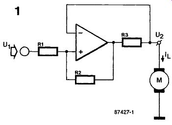
The reverse e.m.f. is directly proportional to the force of the (constant) magnetic field, and the motor speed. In theory, therefore, the motor speed can be held constant with a constant supply voltage. The speed reduction observed in practice arises from the voltage drop across the internal resistance, R, of the armature winding. Thus, when the motor is loaded, its current consumption, and hence VR1, increases, reducing the effective supply voltage. This effect can be eliminated by means of R, compensation, which essentially entails measuring the motor's current consumption, relating this to the motor's instantaneous drop across R1, and increasing the supply voltage accordingly. In fact, this calls for a voltage source with a negative output impedance, since it caters for a higher output voltage when the load is increased.
The basic set-up of the supply required here is shown in Fig. 1. The load current is measured as the drop across sensing resistor Ra. The DC transfer function of this amplifier is written as U2 = U1+ ILR2R3/R1 which accounts for the negative output impedance because then Rout =-R2R3/ R1 For optimum results, this impedance must be kept about equal to that of the motor.
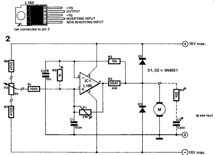
Figure 2 shows the practical circuit of the motor driver based on a power operational amplifier. The Type L165 from SGS can supply up to 3 A at a maximum supply voltage of 36 V, and is therefore eminently suitable for the present application.
Capacitors C1 and C2 suppress noise on the reverse e.m.f. from the motor. Due care should be taken, however, in so extending the circuit, because this readily leads to instability. The motor itself already forms a fairly complex load, since the revolving rotor winding is mainly inductive, and the rotor itself represents a fairly large capacitance. Noise suppression components such as R4 and C3 add to the complexity of the load and may result in control instability, which becomes manifest in the motor's tendency to alternately reverse its direction at a relatively low rate. Also, the response to a fast change in the torque may be impaired, and high-frequency oscillation may occur (noticeable as excessive heating of IC) and/or Ra). When the circuit was tested with a small PCB drill, best results were obtained by omitting Ra-C3 and including C2. If the motor has a noise suppression network, C2 must be omitted, and R5 added to protect the opamp inputs against too high differential voltages as a result of commutation voltage peaks. Clearly, D1 and D2 have been included with this in mind.
Preset P, is adjusted until the motor remains stable.
Over-compensation of the motor will give rise to apparently uncontrolled movement. The adjustment of P, should be carried out when the motor has not yet reached its normal operating temperature, because its self-heating gives rise to an increase in the internal resistance.
The use of a symmetrical supply (± 18 V max.) enables two-quadrant operation of the motor (cw/ccw rotation), which can then be used to power model trains and the like. The motor is halted when P2 is set to the center position. The ground rail may be connected to the negative supply rail if only one direction of revolution is required (PCB drills). The maximum supply is then 36 V, making a greater voltage available for the motor, so that 24 V types can be controlled also, although it is not possible to completely halt these.
The motor can be protected against overloading by selecting a supply voltage that causes the opamp to clip when it outputs the maximum motor current.
Finally, IC, is capable of supplying considerable current, and must, therefore, be fitted with a fairly large heat-sink. The quiescent current of the circuit is about 50 mA.
119 STEPPER MOTOR CONTROL
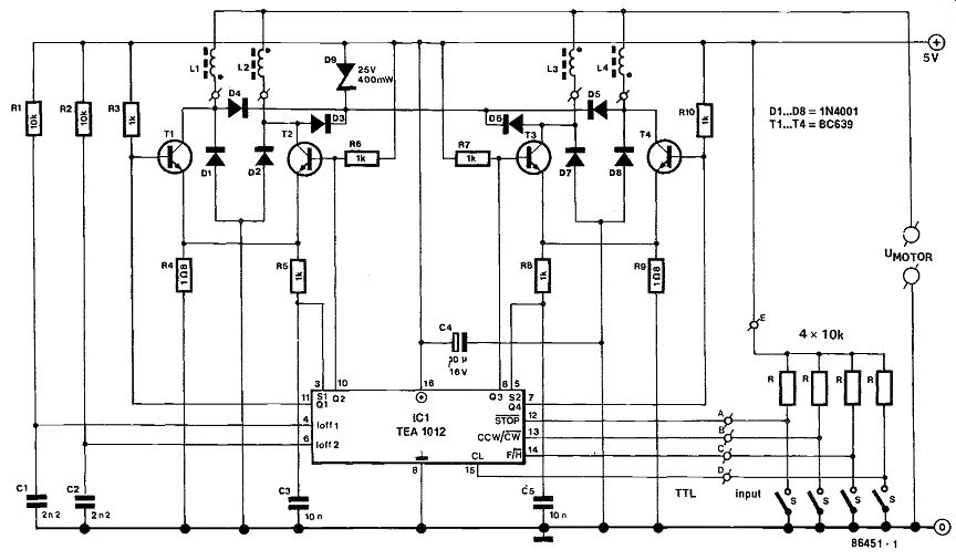
The control of stepper motors is not simple, particularly when no specially designed control circuit is used. The Type TEA1012 is an integrated stepper motor controller that can cope with most if not all situations. In addition to controlling the phases for whole and half steps, it also sets the current with the aid of these phases.
-----------147
Parts list Capacitors:
Semiconductors:
PCB 86451 Ci;C2=2n2 T1;T2;T3;T4=BC639
Resistors:
C3;C5=10 n D1 to D8 incl.=1N4001 R1;R2=10 k C4=10 11;16 V D9 = zener 25 V;400 mW R3;1;t5;R6:R7;R5:R1o= I k IC1=TEA1012 RI;R5=1Q8
The TEA1012 was specially designed for the control of unipolar stepper motors, in which the current passes through the stator windings in one direction. Because the windings behave inductively, the current through them will become too large when the stepping speed is low. The reason for this is that in that situation only the ohmic resistance, which is fairly small, determines the value of the current. To limit the current, a limiting circuit is connected in series with the windings. In the diagram, the current through L1 and L2 is restricted to 0.3/R4, and that through L3 and L4 to 0.3/R9. This enables the current through the stator windings to be adapted to any type of motor.
The table shows in what sequence the various phases are driven with full and half step control, as well as for clockwise and anticlockwise control. The stepper motor is arrested in the position it occupies with the STOP input. CL is the clock input: for each pulse, the motor turns one step forwards or one step backwards.
Because inputs CL, STOP, CCW/CW, and F/H all are 'TTL compatible, it is not difficult to connect these controls to a computer. Resistors R to R14 incl. and the associated switches, enable the circuit to be manually provided with control data.
The maximum stepping speed depends on the type of motor and on switch-off time-constants Ton and Toff(2).
Letters CW and CCW signify clockwise and anticlockwise respectively, while input F/H enables choosing whole (F) or half (H) steps. A double resolution is, therefore, possible.
The supply voltage of the IC may be between 4.5 V and 15 V. The outputs of the TEA1012 are open-collector, so that the operating voltage of the step per motor may be made independent of the supply voltage to the IC.

--------
Table
120 SYMMETRICAL CASCODE OSCILLATOR
Free running as well as crystal controlled clock generators in many digital designs are most frequently based upon the use of one or more inverter gates. However easy it may seem to use these devices for the construction of reliable oscillators, the resultant frequency stability is generally not such as might be expected from a look at the relevant quartz crystal data, and this is mainly on ac count of the rather poorly defined capacitive and/or inductive loading of the crystal at resonance.
Stability, however, may be improved by a factor 3 to 5 by using cascode type inverters in a symmetrical configuration, as can be seen in the accompanying circuit diagram. Two sets of two n- and p-channel MOSFETs, contained in the Type 4007UB IC, have been connected to form a highly stable oscillator circuit capable of operation at frequencies up to 10 MHz, as determined by quartz crystal Xi, which should be a series resonant type.
As the output impedance of the proposed cascode oscillator is relatively high, buffer stage T, has been added to minimize drift with low impedance loads such as (LS)TTL circuits. Furthermore, MOSFET T1 ensures well-defined logic high and low levels to interface with (HC)MOS and (LS)TTL. The values of R4 and R5 depend on the supply voltage level (Ub), while the voltage at gate 2 should be between 4 and 6 V to achieve a 5 V output level swing. In case the oscillator is to operate from a 5 V supply, gate 2 of T1 must be connected direct to + Ub.

-----------
121 THRIFTY LED INDICATOR
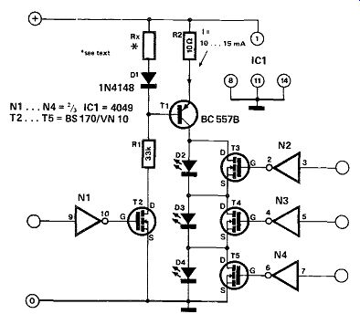
It is often necessary that the current consumption of an essential status indicator is minimal. In the circuit shown, dependent on the level of the supply voltage, a number of LEDs drawing a current of only 10...15 mA may be switched on or off as desired. Moreover, the entire indicator may be switched off if none of the LEDs lights.
The circuit is based on switched current source The base current of this transistor is set at c. 15 mA with Rx. The value of this resistor is calculated from Rx = [4 x 10⁶/(Ub-0.7)] ohm where LA is the supply voltage in volts.
Transistor 12 conducts when the input to inverter N1 is logic 0: when this becomes a logic 1, the current source and, consequently, the indicator are switched off.
If the input to one of the buffers N2 ... N4 is a logic 1, the associated LED is switched on.
More LED-FET combinations may be added to the circuit as long as the supply voltage permits this.
Also, the dissipation of T1 has to be kept within certain limits. A BC557B can be used for T1 over the supply voltage range of 5 ... 18 V.
The circuit is intended for CMOS ICs; if devices of other logic families are used, remember to take ac count of the different logic threshold levels.
Note that the buffers must be powered from the same supply as the current source.
-----------
122 TIME STRETCHER
Anyone with a fascinating hobby must have felt at one time or another that there is not enough time available for his hobby. Any circuit that can stretch those few hours once or twice a week must, therefore, appeal to many.
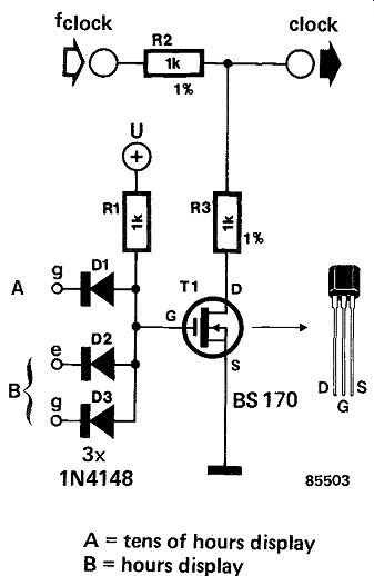
The time stretcher is a small circuit that can be built into almost any digital clock and makes the hobby evening(s) last an hour longer. The three diodes, D1 . . . D3, together with Ri, form an AND gate. 131 is connected to segment g of the tens-of-hours display, and D2 and D3 to segments e and g of the hours display respectively.
When the clock shows 22.00 h, the common line of D1 . . D3 becomes logic 1, because the three segments to which the diodes are connected are "on". This means that T1 conducts and the clock signal of the digital clock is divided by two. The clock then runs at half speed only so that it will take two hours before it shows 23.00 h.
For the circuit to work correctly, it is essential that the clock signal is divided by two exactly, and this means that resistors R2 and R3 must be 1 percent types. This is also the reason that a BS 170 is used as the switching gate; this MOSFET has no saturation voltage. Using a normal transistor with a certain saturation voltage would not cause the clock signal to be divided by two exactly, so that the clock would be fast or slow by minutes within a few days! The circuit as drawn is intended for common-anode displays; if it is to be used with common-cathode displays, simply reverse the connections of diodes D1... D3.
------
A = tens of hours display
B = hours display
123 TRACKING WINDOW COMPARATOR
The use of comparator circuits in many different appearances and practical realizations is common in a wide variety of electronic control and measurement systems. Usually, the voltage from a sensor device is fed to a comparator which, as its name implies, compares the measured level, Ui,,, with a fixed reference, Uref, and produces a negative output (0) or positive output (1) when Um<Uref and Uin>Urer, respectively. A window comparator can be made by connecting two comparators with different reference levels, which define the upper and lower limit of the switching range.
In practice, these references are usually adjusted with presets to dimension the window as required.
This arrangement makes it impossible, however, to automatically shift the window up or down in accordance with, say, ambient light conditions to be measured with a light dependent resistor.
This circuit has no fixed threshold levels, but derives its reference from the measured signal, so that slow changes in this cause the window to track along.
Capacitors C, at the inverting input of A1, and C2 at the non-inverting input of A2 store the input voltage. When the voltage at the non-inverting in put of A1 rises, this opamp toggles. The associated inverting input lags this change because of the delay introduced by the capacitor. LED D, lights.
The process is similar in the A2 section of the circuit when the input voltage drops. This is indicated by LED D2 lighting.
Diodes D3 and D4 form an OR function to actuate a simple relay driver set up with T,. The relay is energized when the circuit detects a fast change in the input voltage. The ability of the circuit to accept a variable input voltage makes it suitable for use in burglar alarms-see Fig. lb. Several break contact arrangements R13-S1-R14 may be connected in series and to the input of the window comparator.
Alarm relay Re, is activated when either S, is opened or S,-R14 is bypassed. To prevent burglars from fooling the alarm, R14 must be fitted into Si, because no alarm signal is given when only S1 is shorted.

---------
The sensitivity of the tracking window comparator is defined by the ratios R2/R3 and R5/R6. The relevant component values indicated in the circuit diagram give 1:100 ratio, so that, for example, a fast change of 30 mV is detected when the input voltage is 3 V. The sensitivity also depends on the input voltage. Although the circuit can in principle handle any input between 0 V and the supply level, the ICs used give reliable operation only when driven between 1 and Ub--1 volt.
The tracking window comparator is preferably fed with a supply between 5 and 15 V. Its current consumption, inclusive of the LEDs but exclusive of the relay, is 10 mA maximum (note that the relay can be fed separately).
124 TRANSMISSION LINES FOR TTL CIRCUITS
Although cable connections between TTL circuits are normally not as critical as those for, say, RF applications, it is still worth while to reflect on this subject because strange things often happen when a TTL transmission line is not correctly terminated.
In particular, this discussion is about terminating coaxial cable and flat ribbon cable. The latter is frequently used for driving Centronics compatible in puts.
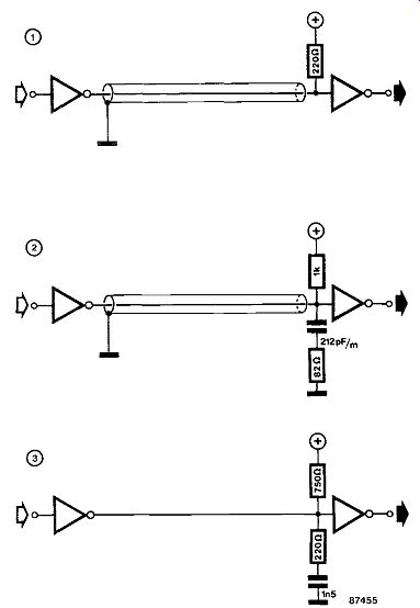
A commonly used coaxial cable is RG59B/U, which has a characteristic impedance of 75 ohm and a propagation delay of 5 ns/m. With signal rise and fall times of 4 ns, the cable may be considered electrically long if it exceeds 40 cm. One of the most common terminations used when driving a long co axial cable with an LSTTL gate is shown in Fig. 1.
This set-up is unsuitable for a HCT bus driver, since the termination provides a poor impedance match, and requires a current sinking capability of 20 mA.
An improved termination circuit is shown in Fig. 2:
this ensures reliable signal transmission for cables up to 15 m. Note that the 1 k-Ohm pull-up resistor is only required when the driver is an open collector gate or buffer.
---------------
Flat ribbon cable often introduces considerable cross-talk between wires, especially when terminated in HC(T) gates, which form a high input impedance. In general, a flat ribbon cable should not be longer than about 60 cm, but longer runs are possible when individual wires are separated by grounded wires (1.8 m max.), or when each wire is terminated with a 1 k pull-up resistor (1.2 m). A combination of these methods makes it possible to use flat ribbon cables with a length up to 2 m, but this is also attainable without ground wires-see Fig. 3. The combined use of this termination net work and grounded wires in the flat ribbon cable should enable a cable length of about 5 m.
125 TUNING AF POWER STAGES
Simple, economically priced audio output stages, such as, for instance, those using the hybrid ICs in the STK series, may be improved in a simple manner as regards distortion, noise, and off-set voltage.
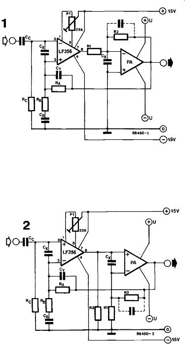
To this end, the output amplifier is included in the feedback loop of an op-amp. Fig. 1 shows the set-up for inverting output amplifiers, and Fig. 2 that for non-inverting ones (the normal situation).
In the calculations to arrive at the new gain of the output amplifier, determined by R1 and R2, it is assumed that the LF356 provides an undistorted signal of 5 Vrms; note also that this type of op-amp must work into a load of not less than 5 kilo-ohms to prevent distortion.
For an output power of 50 W into 4 ohms, the output stage must provide a voltage, U = PR =14.2 Vrms. If the amplification of the stage is 3, the op-amp should deliver 4.73 V. For the set-up in Fig. 1, the value of R2 is then R2= 3R1, while for that in Fig. 2, R2 = 2R1. Note that in both versions only the value of R, should be altered. The total amplification may be calculated from the ratio of RA and Rs as follows: A = (RA + Rs)/Rs.
Furthermore, because of the load impedance of the op-amp, R, >10 k (Fig. 1); R2>10 k (Fig. 2);
RA >10 ohm; and Rc>10 ohm (Fig. 1 and 2).
To compensate for the off-set voltage of the output amplifier, the input capacitor should be replaced by a wire link. The capacitor in series with R, in Fig. 2 should also be short-circuited. The lower frequency limit of the complete circuit is then deter mined by Cs =1/2nfsmRs. The off-set voltage is then smaller than 3 mV, provided both RA and Re are equal to, or greater than, 100 k-Ohm. Where greater accuracy is required, Pl can be used to set the off set to exactly 0 V.
------------
To ensure that there is no direct voltage at the new input of the amplifier, capacitor Cc should have a value of Cc =1/fisnRc.
Since the amplification of the output stage has been reduced to 3, its feedback factor has gone up, and the distortion has gone down. The additional feedback of the LF356 reduces the distortion even further. An overall reduction in the distortion from 1 percent to 0.1 percent is fairly typical.
The altered feedback unfortunately results in a change in stability. If there is a tendency to oscillate, the first thing to do is to bring the upper frequency limit back to its previous value with the aid of Cy =1/2 pi f_lim RA. If the tendency persists, capacitors Cx must be used: their value lies between 100 pF and 1 nF. Our prototype (using STK ICs) worked satisfactorily without either Cx or CY.
126 TWO-FREQUENCY OSCILLATOR

Not so long ago, when semiconductors were still quite expensive, it paid to make a transistor serve more than one function. Although this is no longer necessary because of cost considerations, it is still fun to do so- and it may even have its uses! The circuit presented here is an LC oscillator that changes frequency through reversal of the supply voltage.
When the supply voltage is positive, D1 conducts and short-circuits LAC,. Oscillations are then maintained by crystal XL2 and L2C2. The DC operating point is set by D1 in a way which ensures a compromise between faultless starting of the oscillator and low distortion of the output signal.
When the polarity of the supply voltage is reversed, transistor T1 operates in its inverted mode, i.e., the functions of emitter and collector are interchanged.
This means that the amplification is reduced, but, of course, an oscillator needs an amplification of only just above unity to operate. Crystal XL2 and L2C2 are effectively cut out by D2, and the frequency is now determined by crystal XL, and L1C1.
The circuit lends itself, for instance, for use as BFO switched between USB and LSB.
The crystals may have values of up to 1 MHz.
Current consumption in either mode does not exceed 45 mA.
From an idea in the Master Handbook of 1001 Electronic Circuits.
U= +10 V fx2 U =-10 V-> fxi
127 TWO-GATE BISTABLE
Probably unequalled as to its simplicity given the digital function, this circuit may serve as a single-button on/off control for incorporation in a wide variety of electronic designs. The operation of the proposed bistable is best understood if it assumed that the input of Schmitt-trigger inverter N1 is at logic high level; the output of N2 will therefore be high as well. It is seen that the capacitor is discharged because of the low output level of N,. Therefore, depression of the button pulls the input of Ni to logic low level, causing the bistable to toggle; the capacitor is charged via the 1 M resistor, and the circuit will change state again at the next switch action. The indicated resistor values have been found to offer optimum stability of the bistable, while the use of Schmitt-trigger CMOS inverters is essential to the correct operation.

--------------
128 UP/DOWN CLOCK GENERATOR
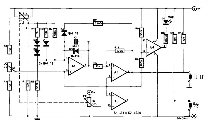
Various designs of clock generators have appeared in previous Summer Circuits issues of Elektor Electronics, and this tradition is kept up with the present design which, unlike the other circuits, outputs an up/down indication as well as a rectangular signal over a wide frequency range; 0 Hz to several kHz.
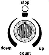
The output signal and the U/D indication are both controlled by a single potentiometer. If this is set to the center of its travel, nothing happens; turning the potentiometer in the clockwise direction causes the U/D output to be at logic high level, and the frequency of the output signal rises with turning Pi further in this direction. The same goes for turning it anti-clockwise, U/D being at low logic level.
The basic operation of the circuit is as follows. Operational amplifiers A1 and A2 together constitute a sawtooth/square wave generator. The falling edge of the sawtooth voltage has a fixed duration of about 200 uS, as defined by the current through D4. The rising edge time, however, depends on the voltage at the wiper of P1. The wiper of P2 is arranged to be at a slightly higher voltage than that at the wiper of P1, when this is set to the center of its travel. The STOP LED will light in this condition. If P1 is turned in either direction, the voltage across R1 rises and causes a low current to flow through R2. This current, and therefore the output frequency, is proportional to the position of the wiper of Pi, but this only goes for a limited frequency range. If the voltage across R2 exceeds about 0.6 V, D1 conducts and connects R3 in parallel to R2. D2 and D3 do the same for R4 at about 1.2 V; this method causes the oscillator frequency to be an exponential function of the voltage, set with Pi; the arrangement ensures a considerable output frequency range for the oscillator A1-A2.
Together with one or more universal counter modules (see Elektor Electronics, March 1985), the proposed clock generator may offer a neat replacement of the well-known BCD coded thumbwheel switches; the potentiometer-set value is present at the Q1 . .Q4 outputs of IC2, as well as visible on the seven-segment display.
-------------
The U/D and clock output of the present generator are connected to the relevant points on the modules, as explained in the above mentioned article, but remember to observe the different supply voltages of clock generator and counter module; keep all points marked + 5V at that voltage, except the supply pin of the LM324 and R14 and It is, which are connected to the counter module +12 V supply. Current consumption of the present up/down clock generator is modest at about 10mA.
129 UP/DOWN COUNTER CONTROL
The up/down binary- or BCD-mode counter is a regularly spotted item in digital circuits of various levels of complexity. The up/down counter simply does what its name indicates; it counts up or down, depending on the logic level applied at the relevant control input, and activates the corresponding output bit pattern at every pulse transition detected at the chip's clock input.
This circuit simplifies the control of up/down counters in that it allows the user to press one but ton to increment the counter output state, while another decrements it. Each of the changeover type buttons is connected to a two-gate de bouncer/bistable (N1-N2 and N3-N4), which sup plies a low pulse at its output when the relevant but ton is pressed. N8, which Serves as an OR gate, receives the debouncer pulses and, together with N8, provides the output clock pulse to the up/down counter.
Bistable N8-N6 keeps track of the selected count mode, and provides the relevant logic level to the up/down counter input. It should be noted that the logic level designation of the up/down input to the counter chip may differ from type to type; it may therefore be necessary to interchange the UP and DOWN keys.
The use of counter chips changing output state on the negative clock transition is to be preferred for use with the suggested circuit, since bistable NB-N8 toggles coincidently with the positive clock pulse transition (see Fig. 2). However a minor disadvantage of the use of negative-edge clocked up/down counters lies in the fact that the circuit acts upon re lease rather than depression of the UP and DOWN buttons.
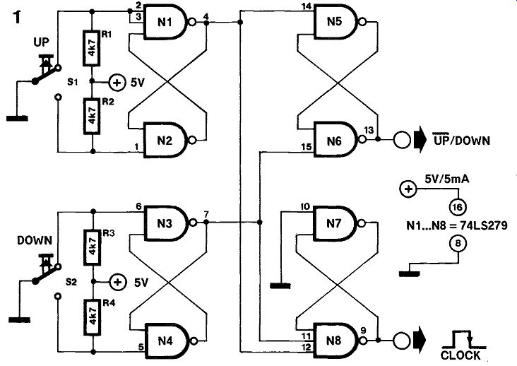
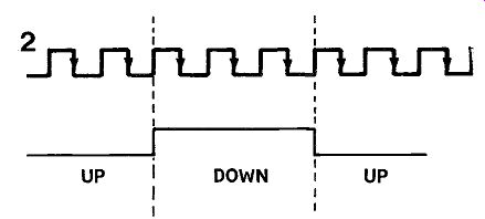
------------
Finally, the use of the Type 74LS279 is in no way compulsory; a combination of other types of TTL IC incorporating the necessary NAND gates should work equally well, but note the three-input NAND gate N8!
130 VERSATILE TIMER
This simple-looking circuit enables the arbitrary programming of seven outputs in a series of not more than 2048 (21t) steps. The step length may be set as required. The time base is derived from the mains voltage. Transistor T produces a square wave from the mains voltage applied to its base.
This square-wave voltage is divided by 10 in IC1, so that the frequency of the signal at the clock input of IC2 is 5 Hz. Circuit IC2 serves as address counter for the Type 2716 EPROM. This means that IC2, after a reset, counts upwards from 0 and runs over the successive addresses of the EPROM.
Circuit IC2 has twelve outputs which would enable the use of a Type 2732 (4096 steps), but, on practical and financial grounds, a Type 2716 is used here since 2048 steps are normally quite sufficient.
The outputs of the EPROM are buffered by a Darlington array, 105, so that seven switch outputs are available with a sink capacity of 500 mA at a maximum voltage of 50 V. The eighth output contains the stop-bit that provides the facility of stopping the program if this is shorter than 2048 steps.
The start-stop circuit is based on bistable N3-N4.
When the supply is switched on, IC2 ensures that the bistable resets from the stop state. This means that both divider IC1 and counter IC2 are in position "zero". The first address in the EPROM must, therefore, have a neutral content, because it is ad dressed in the stop state and thus appears at the output.
The bistable is set, and both resets cleared, when the start button is pressed. Circuit IC1 then commences to divide, and IC2 starts to count. With the present time base, the Programmed content of successive addresses will appear at the output of the buffers at 0.2 s intervals. Counting continues until a stop-bit appears at pin D7 of the EPROM, or stop button S1 is pressed. If required, a HOLD function may be obtained by connecting a switch across capacitor C1, which enables the time base to be switched off.
Switching on a specific output a . . . g merely re quires the corresponding bit position in the EPROM to be left un-Programmed (logic high); programming a 0 disables the relevant output. The stop-bit operates with negative logic: a 0 therefore causes a stop.
Finally, the time base may be adapted for the setting of the required step frequency and accuracy.
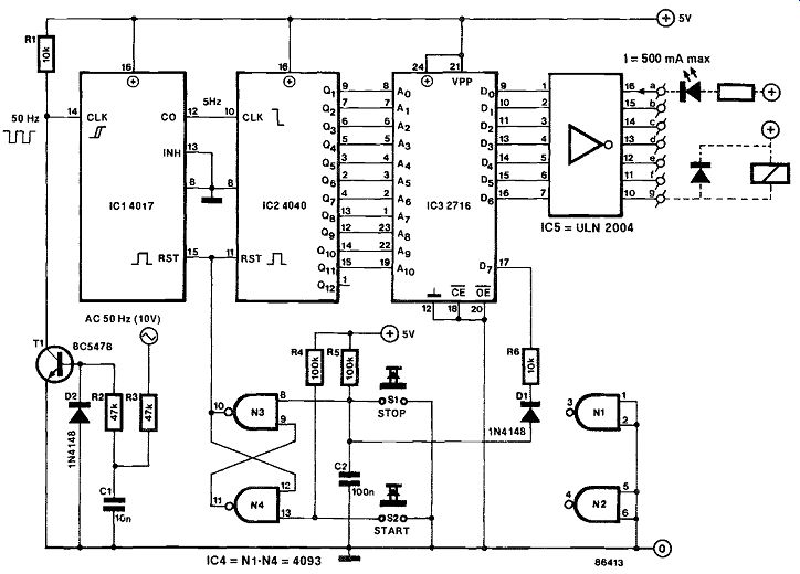
131 VOLTAGE-TO-CURRENT CONVERTER
The converter proposed here (also called voltage-controlled current source) is based on just one opamp, and provides to, or draws from, ground a current that is dependent on its input voltage. The unit can convert negative as well as positive voltages into negative currents (from ground) and positive currents (into ground) respectively.
When a Type 741 or CA3140 is used in the At position, Rv =1 k, and R =10 k, Um= ± 10 V max.; Iout = ± 20 mA max.; and gm =- 1mS. It is, of course, possible to change any or all of these values as required by using a different opamp and altering the values of the resistors. The maximum output current is always dependent on the opamp used. To make such changes, the following formulas may prove useful.
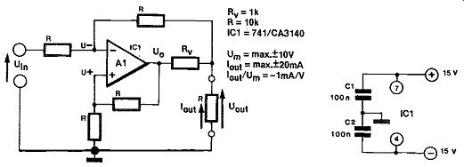
------------
U + = U- = (Um-Uout)/2 + Uout U0= 21(Uin-Uout)/2 + Uout] = Uin + Uout IRv = Uin/Rv Iout = IRv + IR = Uin/Rv + (Uin-Uout)/2R If R> >Rv (the usual case), Lout = Uin/Rv.
---------