143 ELECTRONIC VHF/UHF AERIAL SWITCH
There are many situations where it is useful, or downright essential, to be able to switch between two VHF/UHF aerials at the aerial mast without introducing losses in the signal paths. The switch proposed here does all this over the usual coaxial down lead.
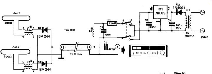
The switch and its small associated power supply are fitted near the relevant receiver. The power supply, consisting of a small mains transformer, a rectifier diode, and a three-pin voltage regulator, provides a direct voltage of 5 V, the polarity of which can be reversed by DPCO (double-pole change-over) switch S1. The poles of the switch are connected to the coaxial cable via decoupling net work L3-C1. Resistor R1 serves as a current limiter for p-i-n diodes D1 and D2. Whichever of these diodes conducts depends on the polarity of the voltage across the coaxial cable. The signal from the aerial connected to the conducting diode is passed to the input of tuner or receiver, while the other signal is blocked.
A p-i-n diode is a semiconductor diode that contains a region of i-type semiconductor between the p-type and n-type regions. They are invariably used as switching diodes. Their most important property is a very low self-capacitance, while at high frequencies they are virtually purely resistive (see Elektor, June 1983, p. 6-36).
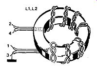
Choke L3 is made from four turns enameled copper wire of 0.3 mm dia. around a ferrite bead. If the aerials have no 75 ohm termination, this may be provided by L1 and L2 which convert the 300 ohm balanced aerial impedance to the asymmetrical 75 ohm required by the receiver input. These inductors are made by winding 7 turns of two-core flat cable on a T50-2, T50-3, or T50-6 toroid as shown in figure 2.
If the switch is mounted in the open, it should be well protected from the elements: potting in araldite is best.
-------------
144 FOUR-WAY AERIAL SWITCH
In many cases it may be necessary to switch between two or more aerials with minimum loss in the RF signal. Though this is not generally a problem at low frequencies, it becomes a serious one when the relevant signal is in the VHF/UHF range (50-960 MHz). The electronic switch described here keeps the switching losses minimal by making use of PIN diodes. PIN diodes are essentially current controlled resistors with properties that make them suitable for switching and attenuating RF signals.
They differ from most other types of diode in that rectification of the input signal only occurs below a certain limiting frequency. Above this frequency, the resistance of a typical PIN diode will change from 1 ohm to 10,000 ohm when the control current is reduced from 100 mA to 1µA.
The circuit can switch up to four aerials, and is composed of two functional parts: the RF switching section, mounted onto the aerial mast, and the power supply & control section, kept near the receiver. In this way, the cost of setting up a multi-aerial system is reduced to some extent thanks to the use of a single downlead cable, instead of as many as there are aerials.
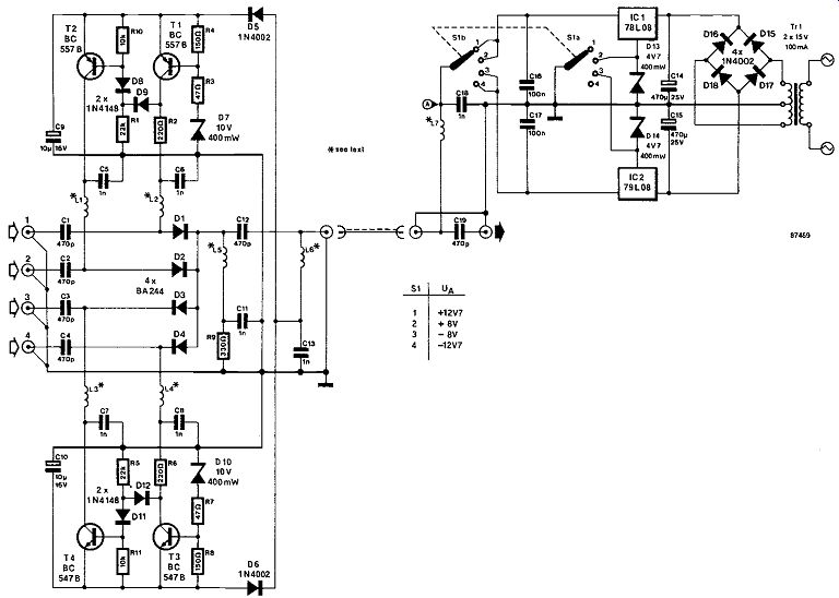
The required aerial is selected by biasing the corresponding PIN diode into conduction. Which of the four diodes conducts depends on the level and the polarity of the voltage applied to the switching unit via the downlead cable to the receiver. When, for example, input 1 is selected with S1, the voltage on the core of the downlead cable is + 12.7 V with respect to the cable screen, and can not reach the circuit around T3 and T4 because D6 does not con duct. The level of the positive voltage causes zener diode D7 to conduct, and so provides a bias for driving it into saturation. T1 in turn provides the requisite bias for PIN diode D1 , and at the same time prevents T2 from conducting. Input 1 is thus connected to the common output of the switching unit, through D1 . If S1 is set to position 2, the supply voltage on the downlead cable falls to 8 V, which is insufficient for D7 to conduct. T1 now re mains switched off, and T2 is driven into saturation, providing the required bias current for the associated PIN diode, D2. Diodes D8 and D9 prevent D1 from being biased through R2 and the base-emitter junction of T2. Input 2 is thus connected to the common output through D2.
Similarly, when the voltage on the core of the downlead cable is negative with respect to the screen, the circuit around T3 and T4 works as outlined above, with either D3 or D4 conducting, depending on the level of the voltage (-8 or -12.7 V).
Inductors L1-L6 prevent the RF signal from being earthed anywhere in the circuit, while L7 prevents it from being short-circuited in the power supply.
For VHF applications of the circuit, 5µH inductors or chokes should be used in the L1-L7 positions, while 21,11-1 types are required for UHF operation.
The RF signal from the selected aerial is passed to the receiver input through C19, which serves to block the direct voltage. In case balanced aerials are to be switched, their outputs must first be made un balanced and, if necessary, transformed to 7552, using a balun.
-----------
The circuit can switch up to four aerials, and is composed of two functional parts: the RF switching section, mounted onto the aerial mast, and the power supply & control section, kept near the receiver. In this way, the cost of setting up a multi-aerial system is reduced to some extent thanks to the use of a single downlead cable, instead of as many as there are aerials.
The required aerial is selected by biasing the corresponding PIN diode into conduction. Which of the four diodes conducts depends on the level and the polarity of the voltage applied to the switching unit via the downlead cable to the receiver. When, for example, input 1 is selected with S1, the voltage on the core of the downlead cable is + 12.7 V with respect to the cable screen, and can not reach the circuit around T3 and T4 because D6 does not con duct. The level of the positive voltage causes zener diode D7 to conduct, and so provides a bias for driving it into saturation. T1 in turn provides the requisite bias for PIN diode D1 , and at the same time prevents T2 from conducting. Input 1 is thus connected to the common output of the switching unit, through D1 . If S1 is set to position 2, the supply voltage on the downlead cable falls to 8 V, which is insufficient for D7 to conduct. T1 now re mains switched off, and T2 is driven into saturation, providing the required bias current for the associated PIN diode, D2. Diodes D8 and D9 prevent D1 from being biased through R2 and the base-emitter junction of T2. Input 2 is thus connected to the common output through D2.
Similarly, when the voltage on the core of the downlead cable is negative with respect to the screen, the circuit around T3 and T4 works as outlined above, with either D3 or D4 conducting, depending on the level of the voltage (-8 or -12.7 V).
Inductors L1-L6 prevent the RF signal from being earthed anywhere in the circuit, while L7 prevents it from being short-circuited in the power supply.
For VHF applications of the circuit, 5µH inductors or chokes should be used in the L1-L7 positions, while 21,11-1 types are required for UHF operation.
The RF signal from the selected aerial is passed to the receiver input through C19, which serves to block the direct voltage. In case balanced aerials are to be switched, their outputs must first be made un balanced and, if necessary, transformed to 7552, using a balun.
145 FRONT-END FOR FM RECEIVER
Among the most important technical characteristics of a VHF preamplifier are the noise figure, and the large signal handling capability. Although these are in principle conflicting requirements, a compromise can be found in the use of high-quality RF components. The receiver's ability to withstand high input levels can be enhanced by providing sufficient selectivity ahead of the active element(s).
This is especially important for the mixer, since it generates most intermodulation products.
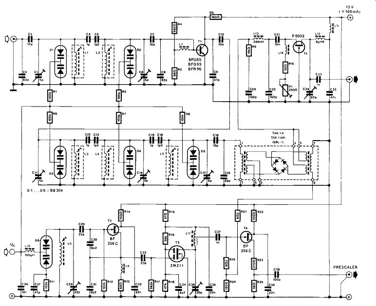
In this FM tuner head, the aerial signal is first passed through a slightly overcritically coupled band filter, amplified with the aid of low noise UHF transistor Ti, and again filtered. The overall gain between the aerial input and the mixer input is about 12 dB at 87 MHz, and 17 dB at 108 MHz. The difference is caused by the adopted method of filter coupling. A wideband Schottky DBM (double balanced mixer) is used for the mixer in this design.
The Type SBL-1 (LO = + 7 dBm) is probably the best available of the 3 DBMs stated. Tuneable local oscillator T2 produces very little phase noise, and DG MOSFET T3 provides a LO power of 50 to 100 mW at a drain current of about 25 mA. FET T4 enables driving a prescaler or a synthesizer with the LO signal. Series network R9-C20 is fitted at the input of the IF amplifier because any passive DBM should be correctly terminated on at least two of its ports. To compensate for the 6 dB conversion loss in the DBM, and to ensure some spare IF gain, medium power RF J-FET T5 is dimensioned to provide a gain of about 12 dB at a drain current of 25 mA.
The proposed front-end gives fairly good results: its third-order intercept point is better than 0 dB when a mixer is used with IP = + 20 dBm, while the noise figure is about 4 dB. This sort of performance should enable the reception of quite weak transmissions even with a powerful transmitter within a few miles from the receiver.
Finally, due account should be taken of the fact that the IF output easily delivers 10 mW, which may well give problems if the IF amplifier is not properly dimensioned.
Inductor data for this project:
L1 ... L5 incl.= E526HNA10014 (Toko).
L6= E526HNA10013 (Toko).
L7 ...L9;L14 = 6 turns 36SWG (0 0.2 mm) enameled copper wire through a ferrite bead.
L,1= 9 turns 24SWG (0 0.6 mm) enameled cop per wire on a T25-12 ferrite core; tap at 3 turns from C35-R15-R16.
--------------
146 FRONT-END FOR SW RECEIVER
There are many conflicting technical requirements for a good-quality front-end in an SW receiver. The noise figure and the intermodulation level should be low, the RF insulation between ports LO, RF and IF should be high, and some amplification is desirable. The Type SL6440 high level RF mixer from Plessey ensures a noise figure of around 10 dB, and offers sufficient suppression of the LO signal.
The signal applied to the RF input (B) of the front end is passed through a low-pass filter with a cut-off frequency of 32 MHz and an output impedance of 500 ohm. The open collector output of mixer IC, has a relatively high impedance, which necessitates the use of Tr1 and R5 for correct matching to 48 MHz crystal filter FL,. The fixed impedance of this filter for signals outside its pass-band helps to keep the intermodulation distortion low. Trimmers C13 and C14 are aligned for a maximum flat pass-band at minimum loss. The mixer's intermodulation characteristics can be optimized by careful dimensioning of R, and R2, provided the amplitude of the local oscillator signal is stable. A third-order intercept point of 33 dBm was achieved in a prototype. The mixer IC gets fairly warm, and should be cooled with a heat-sink.
The RF transformers are wound as follows (use 30SWG enameled wire):
Tr1: the primary winding is 10 +10 bifilar turns, the secondary is 10 turns, on a Type T50-12 ferrite core.
Tr2: the primary winding is 2 turns, the secondary 18 turns, on a Type T50-12 ferrite core.
Ls: 6 turns through a ferrite bead.

------------
147 HIGH LEVEL PASSIVE DBM
The mixer is one of the most important sections in any good-quality SW receiver, since it determines to a large extent the sensitivity and the dynamic range.
The so-called switching mixer is often used, because it has none of the technical imperfections of active mixers. The most commonly found switching mixer is the diode-based double balanced type (DBM), which is, unfortunately, a notoriously expensive component, especially when a high intercept point is required to ensure low levels of intermodulation.
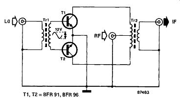
The application of active devices, such as bipolar transistors and J-FETs, in a passive mixer is less well established. And yet, these components enable the mixer to remain relatively simple, since the RF in put signal can be thought of as electrically insulated from the local oscillator output. The present design is based on a pair of well-known UHF transistors, which require no supply voltage or bias circuits.
The input and output transformers are wound on two-hole ferrite cores (Baluns). The primary of Tr2 is 8 turns with a center tap for the RF input, the secondary is 4 turns. Tr1 is wound such that the indicated LO amplitude is available at the secondary.
Only the RF input or the IF output requires correct termination on 50 ohm, the other connections are then fairly uncritical. The input intercept point of this mixer is excellent at between 31 and 36 dBm, while the noise figure and conversion loss are acceptable at about 6 dB. The ID rejection is roughly 25 dB, and depends mainly on the construction.
The mixer is suitable for RF and IF signals up to 30 and 50 MHz respectively.
------------
148 HIGH LEVEL WIDEBAND RF PREAMPLIFIER
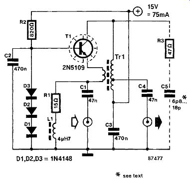
A linear RF amplifier can be made in two ways: (1) with the aid of a linear active element, or (2) with a non-linear element operating with negative feed back. This circuit is of the second kind, using an RF power transistor as the active element. Feedback is also required to ensure correct termination (50 ohm) of the aerial, since bipolar transistors normally exhibit a low input impedance. Also, the noise figure is not increased because virtually no signal is lost.
The common-base amplifier is based on a UHF class A power transistor Type 2N5109 from Motorola. The feedback circuit is formed by RF transformer Tr1. The input and output impedance of the preamplifier is 50 ohm for optimum performance. Network R3-05 may have to be added to preclude oscillation outside the pass-band, which ranges from about 100 kHz to 50 MHz. The gain is approximately 9.5 dB, the noise figure is between 2 and 3 dB, and the third-order output intercept point is at least 50 dBm.
----------------
The input/output transformer is wound on a Type FT37-75 ferrite core from Micro-metals. The input winding is 1 turn, the output winding 5 turns with a tap at 3 turns.
149 LOW NOISE AERIAL BOOSTER
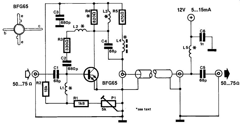
After having read the design essentials relevant to wideband amplifiers, RF filtering, intermodulation/cross-modulation characteristics, etc., as given in the articles listed at the end of this article, there would seem to be little need for us to dwell on functional and electronical aspects of the present ultra low-noise, wideband preamplifier incorporating the wonderful Type BFG65 transistor, which, although already introduced in [3], deserves to be put in the RF limelight as it offers an exceptionally low noise figure at more than satisfactory strong signal response, thanks to the relatively high collector current (Fa = 0.8 dB at 5 mA, for instance).
----------
----------
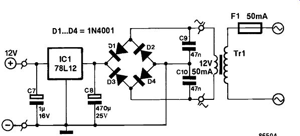
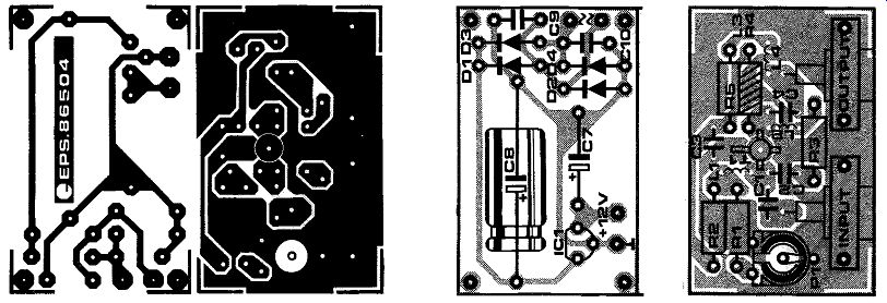
Since the important points to observe in RF construction have been covered in [1] and [2], the large earth plane on the component side of the ready made PCB Type 86504 need not cause any wonder; all parts are soldered direct onto the relevant copper fields; the holes merely serve to aid in locating the parts correctly. The hole for T1 should be drilled to dia 5 mm for the transistor to be seated and soldered with the shortest possible lead length.
Additional holes have been provided to enable the input and output coax cables to be secured by means of screw-on clamps, although soldering screen and core should also be possible.
It is seen that the ready-made PCB consists of an RF and a supply section, which may have to be separated by cutting if it is desirable to fit the units at different locations, as is the case with a masthead mounted amplifier and the supply located at the nearest mains outlet, e.g. on the attic. On the other hand, if is more convenient to cut the downlead cable immediately as it appears indoors, amplifier and supply may be left to form one unit for insertion in the coax cable. As in that case the amplifier may be fed direct rather than via the coax cable core, L4, L5, C5 and C6 are rendered unnecessary and may be removed; the free lead of R5 should then be connected to the +12 V terminal on the supply section of the board.
The optimum collector current for T1 is adjusted by means of P which should be set for a value between 5 and 7 mA if the amplifier is to handle relatively weak signals, such as may be received in fringe areas. The indicated collector current corresponds to 2.3 to 3 V voltage drop across R5; higher values (10 to 15 mA; 4.6 to 6.1 V respectively) should be set when receiving two or more strong (local) transmissions in the 80 .. . 800 MHz band.
If masthead-mounted, the amplifier should be fitted in a waterproof enclosure, carefully treated with silicone spray to preclude corrosion of the solder contacts.
Finally, the coils are wound as follows, using dia 0.3 mm (30 SWG) enameled copper wire:
L1: 8 turns, closewound, internal dia 3 mm.
L2: 4 turns, closewound, internal dia 3 mm.
L3: 5 turns on R4.
L4; L5: 4 turns through 3 mm ferrite bead.
Literature references:
[1] VHF filters (EE, March 1986, p. 50 ff).
[2] VHF amplifier (EE, April 1986, p. 40 ff).
[3] Wide band amplifier for satellite TV receivers (EE, April 1985, p. 66 ff).
[4] Aerial amplifiers (EE, February 1980, p. 27 ff).
Parts list
Resistors:
R1 =1k8
R2 =18 k
R3 = 330
R4 = 820
R5 = 470 52
P1=5 k preset
Capacitors:
C1;C3;C5= 68 p
C2;C3= 680 p
C6 =1 n
C7=1 u / 16 V; electrolytic
C8 = 470 u;25 V; electrolytic
C9;C10 =47 n
Semiconductors:
D1 ... D4=1N4001
IC1 =78L12
= BFG65 (Philips/Mullard)
Miscellaneous:
L1 ... 1_5= see text.
Tr1 = 12 V;50 mA.
F1 = 50 mA; fast.
PCB Type 86405.
4 soldering pins.
150 MORSE FILTERS
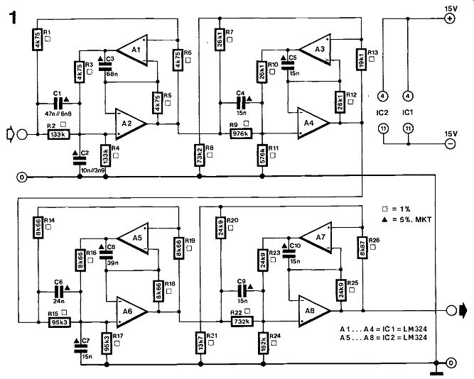
Morse, or CW (continuous wave), is still widely used thanks to the fact that the necessary equipment can be kept relatively simple, and therefore in expensive, if the operator is sufficiently trained in selective listening. A morse decoding computer, however, requires an adequately filtered input signal, because it lacks the noise discriminating capability of the human ear. Some receivers can be upgraded with a 250 Hz IF filter for this purpose, but such an extension is usually well beyond the financial reach of most radio amateurs. The filters discussed here operate in the audible frequency range, and compare favorably with far more expensive types for 455 kHz. Figures 1 and 2 show the circuit diagram and the typical response of an eighth-order inverse Chebyshev filter which has been optimized for non-computer using listeners.
The filter of Fig. 3 is less complex, and intended for driving a computer. The associated frequency response is shown in Fig. 4. Both filters were designed with Eldesign IIe, an advanced filter design program for the BBC micro. The inverse Chebyshev response gives a smooth pass-band, while the characteristic ripple ends up in the stop band. This ensures the required phase stability in the passband, which is a must for processing burst-like signals such as morse.
Prototypes of the filters gave excellent results: normally hardly audible signals could be recovered for reliable decoding. The supply for the filters is preferably a symmetrical 15 V type to ensure an optimum dynamic range. Do not use any other opamp than the LM324, since types with a higher cut-off frequency may give rise to oscillation. Note that C1 in Figs. 1 and 3, and C2 in Fig. 1, is a parallel combi nation of two capacitors from the E12 range of values, while all resistors used are from the E96 range. Should any of the filter sections persist in its tendency to oscillate, either one of the even-numbered opamps may have to be dimensioned for a slightly different roll-off point by connecting a 100 pF capacitor across the output and the input, and a 390 ohm resistor between the input and junction C3-R5-(-A1) (example refers to opamp A2).
---------

----------
151 MULTI-MODE µP-CONTROLLED IF MODULE
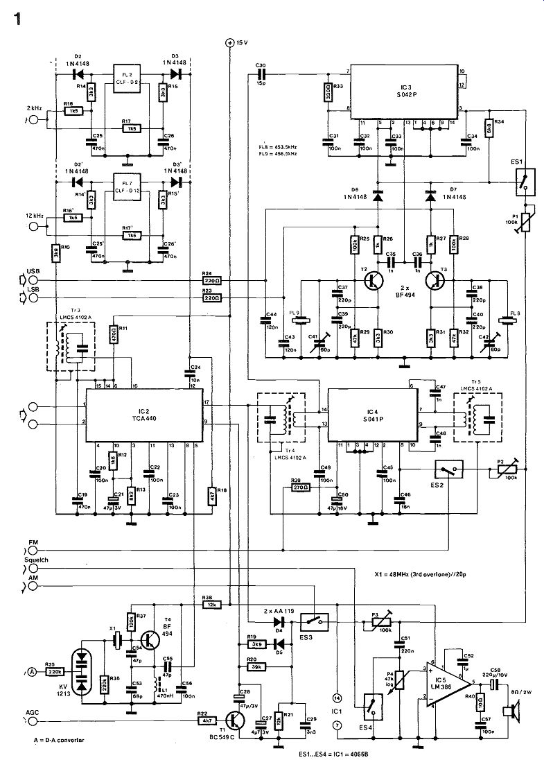
The intermediate frequency (IF) module shown in Fig. 1 accepts 48 MHz, and is suitable for receiving AM, FM and SSB transmissions. CW reception should also be possible in the SSB mode when a sufficiently narrow band-filter is included (BW<500 Hz). For radio-teletype (RTTY), it is best to drive a comparator from the FM detector output.
There is no need for a high level mixer to convert the input down to 455 kHz, since the 48 MHz signal has already been filtered and occupies a bandwidth of only 12 kHz. The RF and mixer stages in the TCA440 operate up to 50 MHz, while the built-in AGC has a dynamic range of about 100 dB. The mixer output is fed to diode switches to enable digital selection of the appropriate band width.
----------
----------
The proposed selection circuit ensures a filter separation of the order of 80 dB. The choice of the 455 kHz filters is governed by the particular application and the financial means available. The CLF D12 and CLF-D2 are for FM/AM and SSB respectively: the number in the type indication stands for the bandwidth. The Type CLF-D4 or CLF-D6 can be used equally well for communication quality AM. Unfortunately, narrow-band filters for CW and RTTY are difficult to obtain, but "add-on" 500 Hz or 250 Hz filters for commercially available receivers and transceivers (Yaesu, Kenwood) can be used here with excellent results.
The IF output from IC2 is rectified for the AM and AGC sections, and inductively fed to FM detector IC4 as well as to product detector IC3. Note that in general no AGC action is required in the FM and RTTY mode. The BFO for the product detector is based on USB and LSB ceramic resonators, which are found in most SW receivers of Far Eastern origin, but may be difficult to obtain as a one off.
The circuit around T4 is a voltage-controlled 48 MHz crystal oscillator (VCXO) that operates in the parallel mode, requiring due attention to be paid to the correct output frequency if a common, series-resonant crystal is used. The synthesizer for tuning the proposed receiver outputs 1 kHz steps, so that a D-A converter is required for driving the VCXO input. A resolution of 10 Hz should be adequate to ensure smooth and reliable tuning.
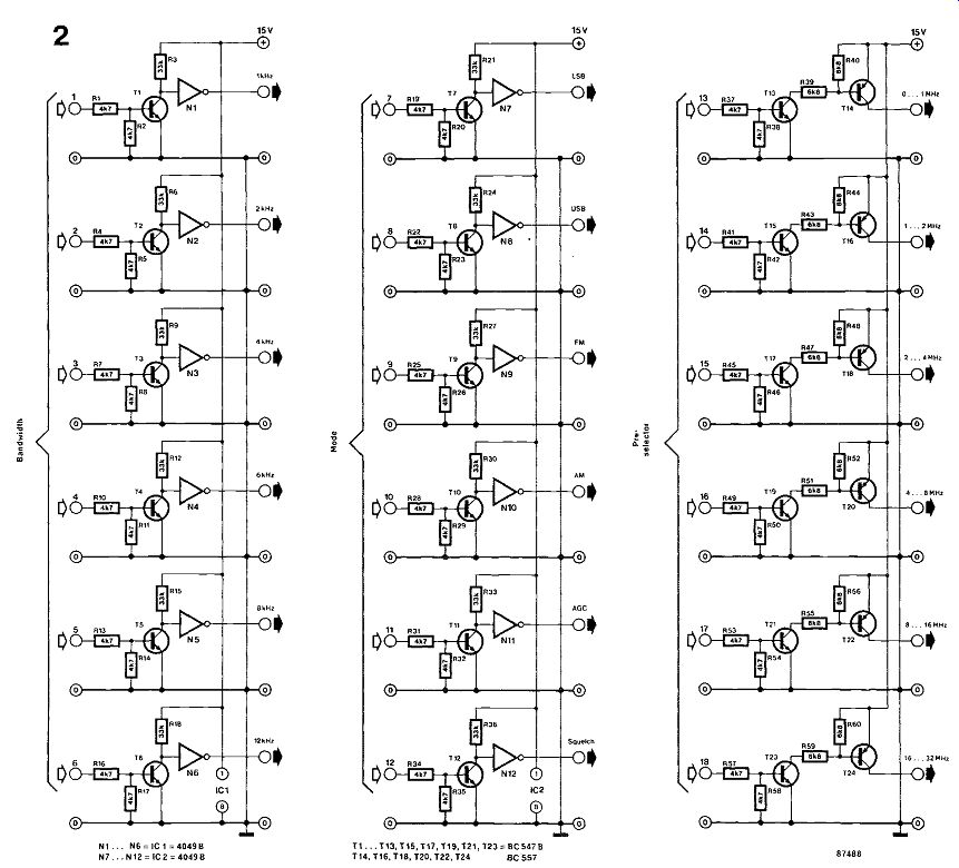
The computer interface for controlling the receiver is shown in Fig. 2. This is essentially a 5 V to 15 V logic level converter with TTLICMOS compatible control inputs. The remote control of the receiver obviates the need for this to be housed in a neat enclosure. Albeit that the receiver therefore need not have a "desktop" appearance with all the controls fitted on a front panel, it is, of course, still necessary to provide for adequate screening and thermal stability. Sufficient AF power is available from 105 to drive a relatively long cable to the loud speaker enclosure, which is located near the computer.
The receiver can be controlled from any computer that has three 8-bit output ports based on, for in stance, Type 74LS374 octal latches. A receiver function is enabled when a logic 1 is written to the respective input. Example: 4 kHz bandwidth is selected by driving BANDWIDTH input 4 high, and the remaining five low. Writing a computer program for controlling the receiver should not be too difficult if the following sequence is observed: 1. actuate the squelch; 2. reset all bits on the relevant control port; 3. set the required bit; 4. turn off the squelch.
152 NOISE BLANKER
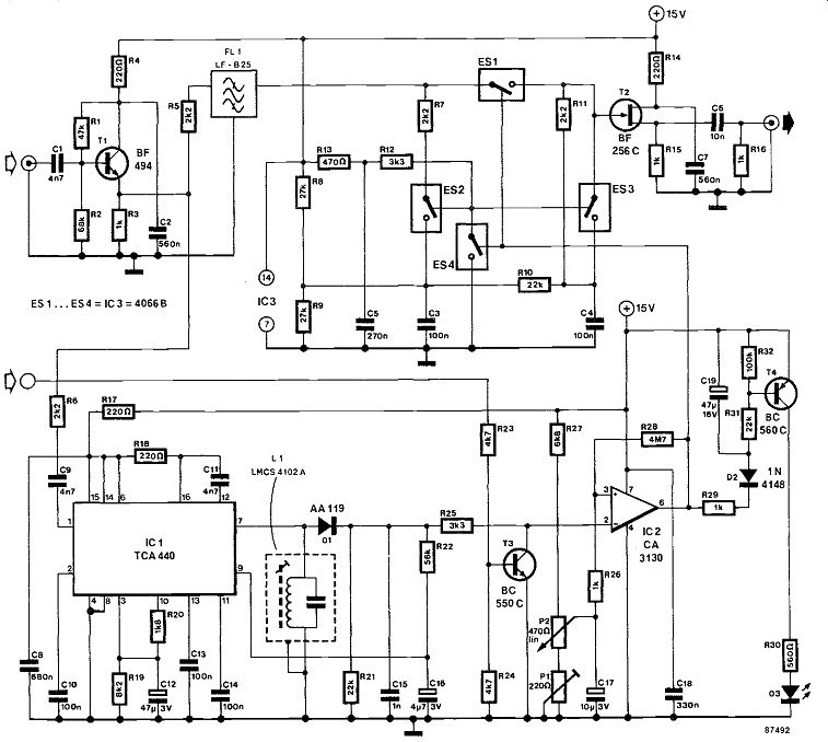
A noise blanker is indispensable for improving the reception of very weak signals on the SW bands. In most communication receivers, the selectivity of intermediate frequency (IF) filters cause interfering pulses to be widened, blotting out the wanted signal. It is useful, therefore, to suppress interference before this can wreak havoc in the IF sections of the receiver.
The 455 kHz IF signal is first buffered in T2, and then processed separately in two circuits.
The lower section of the circuit is a TCA440 based receiver for the interfering pulses. The TCA440 is in itself a virtually complete receiver, since it comprises an RF amplifier, a mixer, and an IF amplifier.
All stages in the latter are used since pin 4 is grounded here. The pulse receiver has its own AGC (automatic gain control) to ensure effective suppression of relatively weak interference also. Preset Pt and potentiometer P2 enable precise adjustment of the noise blanker for various levels of interference.
The circuit can be controlled digitally via R23; a logic high level renders the noise blanker ineffective.
The interfering pulses are made logic compatible with the aid of opamp IC2. LED D3 lights when noise is detected.
In the upper section of the circuit, the IF signal is first delayed in FL1 to compensate for the processing time in the pulse receiver. ES1 is opened when a sufficiently strong interfering pulse is recognized, so that the IF signal is no longer applied to output buffer T2. Also, the gate of this FET is then grounded for RF signals via ES3-C4, while ES2 is closed to maintain correct termination of FL1.
Properly constructed, this circuit achieves noise suppression of the order of 85 dB. Alterations to suit operation at an IF other than 455 kHz involve L1 and FL1, although due account should be taken of the parasitic capacitance of the electronic switches at relatively high frequencies.
------------
153 NARROW-BAND IF FILTER
Since good crystal filters are expensive, there is a constant search for (less expensive) alternatives.
One of these is the ceramic filter, now widely used as IF filter in short-wave receivers. The somewhat poorer temperature characteristics of ceramic filters (as compared with those of crystal filters) are normally not of much consequence.
Numerous experiments have finally led to the circuit of Fig. 1, which uses five 455 kHz ceramic filters. As computer crystals can be obtained cheaply nowadays, it would also be possible to construct a similar filter with a number of such crystals.
The result of our experiments is a 3 dB filter band width of about 800 Hz; the attenuation outside the pass-band is of the order of 60 dB.
A possible application is its use in a receiver with variable bandwidth for SSB, AM, and FM operation.
Another application is as input filter in a receiver whose dynamic frequency range is inadequate (but the IF should then not be 455 kHz).
Finally, note that correct matching of both the in put and output impedance (330 ohms) is imperative.

154 NAVTEX RECEIVER
NAVTEX, the international maritime service that provides navigational and meteorological information via RTTY (radio teletype) on 518 kHz, makes use of FECTOR. This is a system in which the information is transmitted twice, with a particular interval between the first character and the repeat. FECTOR is decoded automatically by a microprocessor that is coupled to the ship's medium wave receiver.
It is, of course, not desirable that the decoder is taking up the medium wave receiver continuously.
On the other hand, navigational officers, and many amateur radio listeners, do not want to miss one iota of NAVTEX information. Obviously, a second receiver is the answer, and this can, of course, be coupled to the decoder night and day. Since only one frequency, 518 kHz, and one type of trans mission, FSK (frequency shift keying), needs to be received, the circuit can be kept quite simple.
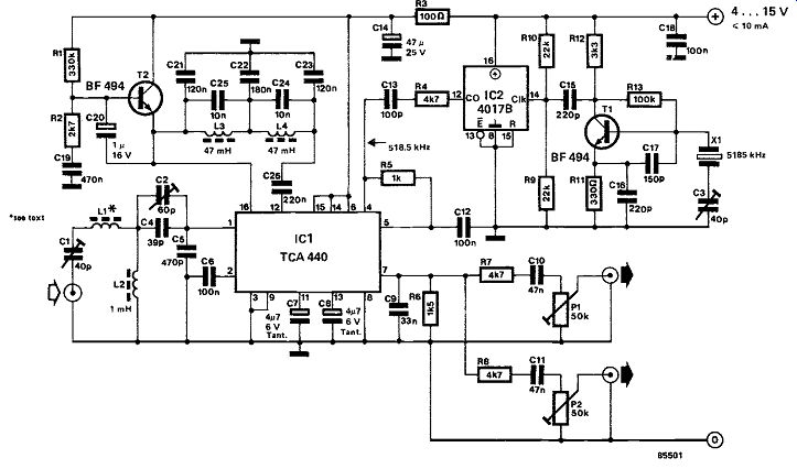
The circuit is based on a type ICA440. The AGC (automatic gain control) provided by this IC is not used because the IF amplifier, due to its internal symmetry, is already an excellent limiter for FSK signals.
The internal oscillator is not used either: it is re placed by a crystal oscillator, T,, operating on 5185 kHz, that is followed by a decade scaler, IC2.
The exact frequency of the crystal depends on the requirements of the decoder; trimmer C3 enables it to be varied by a few kHz, i.e., a few hundreds of Hertz at the output.
Thanks to the TCA440, the remainder of the receiver is fairly simple without the need of special components. Standard chokes can be used in the L2 . . .L4 positions; L1 consists of 6 turns enameled copper wire of 0.3 mm dia. on a ferrite bead.
Sensitivity of the receiver is good at a few AN.
Calibration is very simple: adjust input trimmers C1 and C2 for maximum output, and then turn C3 until the output frequency matches the decoder.
The crystal should be suitable for parallel resonance with a capacitance of 30 pF.
Current consumption is not greater than 10 mA.
The supply voltage may be 4 . . .15 V.
It is, of course, a fairly simple matter to make the receiver suitable for use on other maritime medium wavelengths.
-----------
155 RTTY CALIBRATION INDICATOR
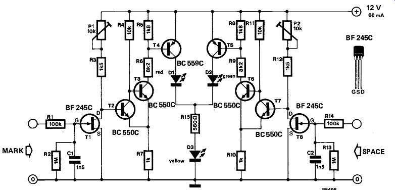
To calibrate an RTTY (radio teletype) decoder correctly in accordance with the marks and spaces, an oscilloscope is needed. The mark and space signals are applied to the X and Y inputs of the instrument respectively, when, on correct calibration, the screen of the oscilloscope displays the well-known RTTY cross.
----------
If an oscilloscope is not available, the circuit shown here can be used. It consists of two amplifiers with high-impedance input, T1 and TS that are followed by driver stages T2 . . T4 and T5 . . . T7. The driver stages control three LEDs, D1 . . D3 direct. Diode 131 (red) is the mark indicator, D2 (green) is the space indicator, and D3 (amber) indicates whether the decoder has been calibrated symmetrically.
Preset potentiometers P1 and P2 determine the amplification of the field-effect transistors. Proper set ting of these components enables the indicator to be matched with the filter outputs of any RTTY decoder.
After the indicator has been coupled to the RTTY decoder, that unit can be calibrated as follows: tune the short-wave receiver to the marks; the BFO knob must be adjusted until the red and amber LEDs both flash brightly; the RTTY decoder is then adjusted to the correct frequency deviation, indicated by the flashing of the green LED. If the amber LED lights continuously, the decoder has been calibrated correctly.
Otherwise, the above procedure should be repeated carefully.
156 RTTY/CW FILTER
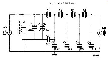
An appreciable part of short-wave radio traffic takes place via morse and radio teletype transmission. To ensure optimum reception of these types of trans mission, a practical bandwidth of about 300 Hz is required in the receiver. Such a bandwidth allows for some drift of both transmitter and receiver, and also for the frequency shift of RTTY signals. As commercially available filters meeting these requirements are still rather expensive, it pays to build your own: a suitable one is shown in the accompanying diagram.
The crystals used are inexpensive types, commonly found in computer systems.
Inductor L1 is made by winding 2 times 20 turns enameled copper wire of 0.3 mm diameter onto a T50/2 RF toroid (available from Cirkit).
Some parameters of the filter are:
bandwidth at -6 dB points : 300 Hz
bandwidth at-60 dB points : 1100 Hz II insertion loss : 7 dB II ripple in pass-band : 1 dB
-----------
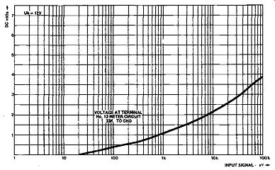
157 S METER
Since many amateur receivers are fitted with an S meter that functions far from logarithmically, the proposed circuit should be a welcome extension of such receivers.
Although ICs such as the CA3089 or the CA3189 are not in common use any more, they serve a useful purpose in the meter circuit, because, apart from a symmetric limiter, a coincidence detector, and an AFC amplifier, they contain a very good logarithmic amplifier-detector.

----------
--------
As is seen, the circuit is fairly simple, but remember that these ICs operate up to about 30 MHz, so that the wiring of the meter, and also its connections in the receiver, should be kept as short as possible.
Note further that the input of the CA3189 must be terminated by 50 ohm; the connection to the input of the CA3189 should be in screened cable; if it is not possible to obtain the input signal from a low-impedance source, a source follower should be used between it and the meter circuit.
158 SEND/RECEIVE IDENT
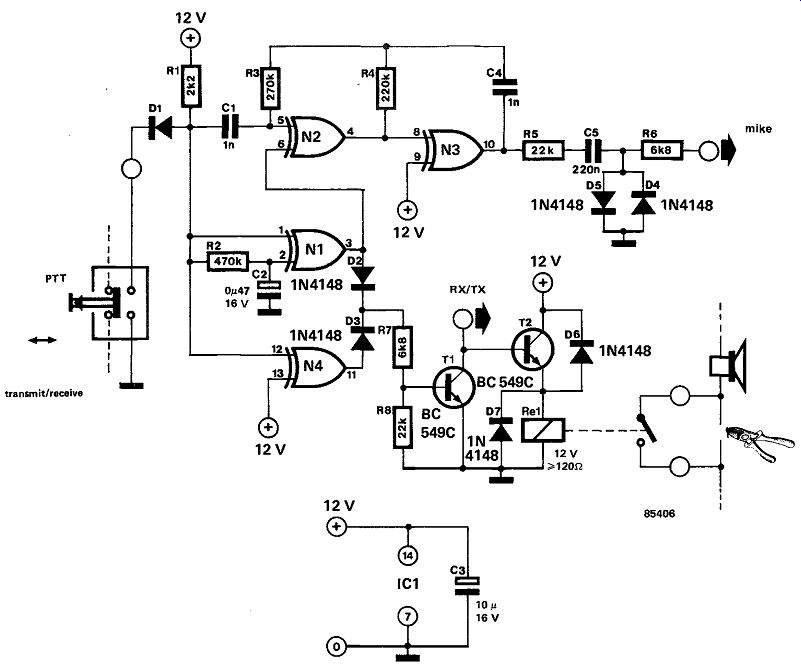
Some radio amateurs like to give an identification signal at the beginning and end of a message; others frown upon this practice which they find disturbing. If you belong to the first group, you may find this circuit useful as it gives an ident signal automatically when the transmit/receive key is pressed and just after this has been released again. The two signals are identifiable by being slightly different in frequency.
XOR gate N, functions as a monostable, whose output is high for a short time after its inputs either change from high to low (at the onset of a trans- mission), or from low to high (at the end of a trans mission). Its output is applied to an oscillator, N2/1\13, and to the transmit/receive switching section. When the input pin 6 of N2 is high, this XOR gate functions as an inverter, so that the oscillator generates a short tone in the medium audio range which is fed to the microphone via limiter D4/D5.
The frequency determining network is earthed via C1 and D1 or via C1 and R1, depending on whether the transmit/receive key is pressed or has just been released.
During transmission, the rx/tx output is low: this output is intended to be connected to the corresponding input of the transceiver. Transistor T2 is on, so that relay Re, is actuated: its contact(s) may be used, for instance, to disconnect the loudspeaker during transmissions.
Current consumption, ignoring the relay current, amounts to about 15 mA.
159 SIMPLE FIELD STRENGTH INDICATOR
------------
A practically proven small circuit that is very popular with many model fliers, as it enables them to verify that their remote control transmitter is actually transmitting. Any doubt as to whether a fault lies in the receiver or transmitter is also quickly resolved.
The only active element in the circuit is a transistor that is used as a controlled resistance in one of the arms of a metering bridge. The base of the transistor is connected to the wire or rod aerial. The increasing HF voltage at the base of the aerial drives the transistor so that the bridge is brought out of equilibrium. A current then flows through R2, the 0.5 1 in mA meter, and the collector-emitter junction of the transistor. The meter should be zeroed with P1 before the transmitter is switched on.

160 SPOT FREQUENCY RECEIVER
Monitoring a number of frequencies in the short wave band, such as the international shipping distress frequency, is a fascinating pastime. Since only a limited number of stations is normally monitored, and their frequency is invariably fixed by international treaty, the receiver needs only to be capable of being switched between those spot frequencies.
The receiver works on the direct conversion principle, i.e., the oscillator frequency is equal to the received frequency, so that the intermediate frequency is zero.
The aerial signal is fed to tuned RF amplifiers T1 and T2 via a switched preselector. The RF amplifiers are coupled to an S042P type mixer.
There are three crystal-controlled local oscillators, which are switched into circuit in accordance with the preselector.
The output of the mixer is the audio signal, which is fed to AF amplifier IC2 via low-pass filter R11, R13-C28. C30. The gain of IC2 is about 60 dB.
Part of the output of IC2 is rectified in D1 and D2 and used for AGC (automatic gain control) of T1 and T2 The output of IC2 is fed to power amplifier IC3 which drives a loudspeaker or headphones. There is also a tape output. Volume control is provided by 13% Inductors L1 . .L3 are each wound on a T50/2 toroid as follows:
L = 115 turns enameled copper wire of 0.15 mm dia. with tap at 11 turns; L2, L3 = 90 turns enameled copper wire of 0.2 mm dia. with tap at 9 turns.
If different frequencies from those shown are required, one or more of the crystals must, of course, be replaced, but at the same time L1, L2, or L3, as appropriate, must also be modified. The change in the number of turns and the tap is directly proportional to the change in frequency. If, for in stance, a frequency of 2600 kHz instead of 2182 kHz is wanted in position 1 of switch Si, the number of turns, n, of L1 should become n= 115(2182/2600) = 97 turns and the tap should be at n =11(2182/2600) = 9 turns.
Oscillator capacitors C4, C6, and C8 should have a higher value if the frequencies are chosen at the low end of the short-wave band.
When the receiver has been built correctly in accordance with HF requirements (short connections, ample decoupling), it should work up to about 18 MHz. The dashed lines in the circuit diagram represent earthed screens between the various sections.
The receiver is calibrated by adjusting C5, C7, and Cs for zero beat, and then adjusting C1, C2, and C3 for maximum audio output.

---------------
161 SWITCHABLE BANDSELECTOR
-------
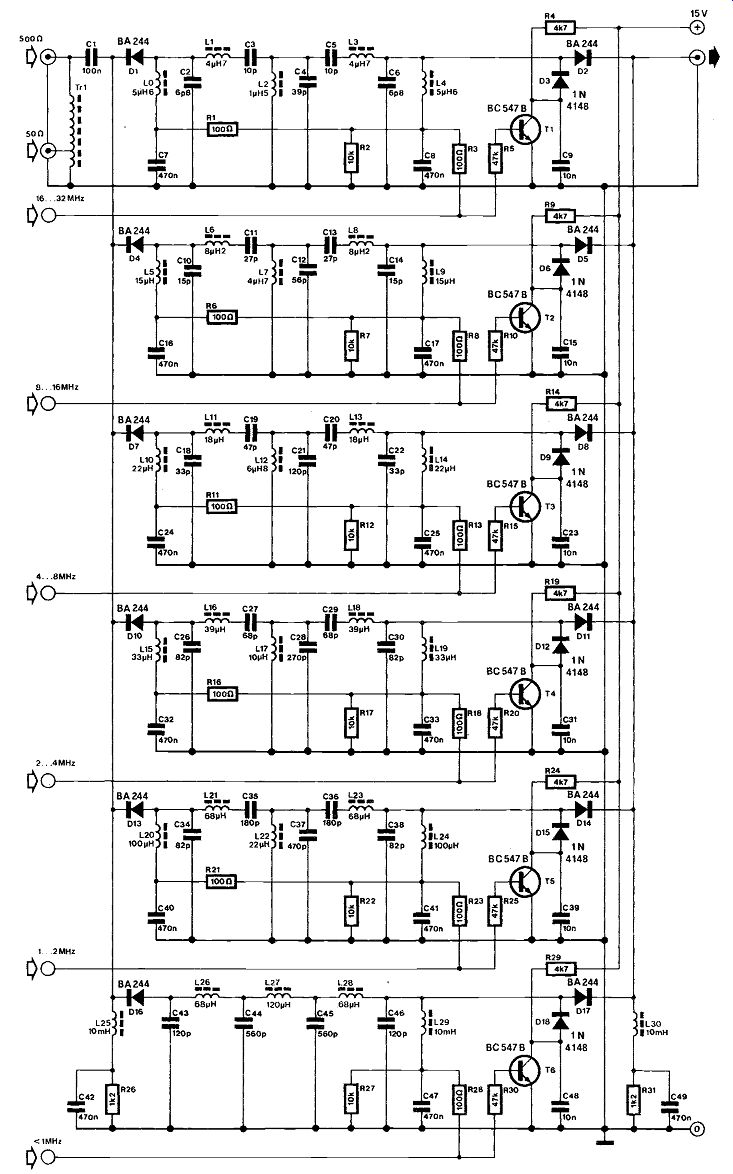
In many older types of SW receiver, intermodulation in the mixer was generally avoided by including a tunable, often automatically tracking, pre-selector. In a computer-controlled preselector, the use of varactor diodes for tuning the inductors often leads to considerable intermodulation distortion. A different approach is therefore used in this design.
The circuit diagram shows the use of PIN diodes Type BA244 for selecting one of 5 band filters followed by a low-pass section. Selection of a filter is effected by having the computer drive the associated input high. An impedance transformer is provided at the input to enable connection of 50 ohm as well as 500 ohm aerials. For most purposes, the 500 ohm input is preferable, since it allows short aerials to be correctly terminated. Input transformer Tri is wound on a ferrite core Type FT37-75 from Micro-metals. The total number of turns is 19, with a tap at 2 /2 turns from the ground connection. The input should be provided with an overvoltage protection if the aerial is a large, outside mounted, array.
162 SYNTHESIZER FOR SW RECEIVER
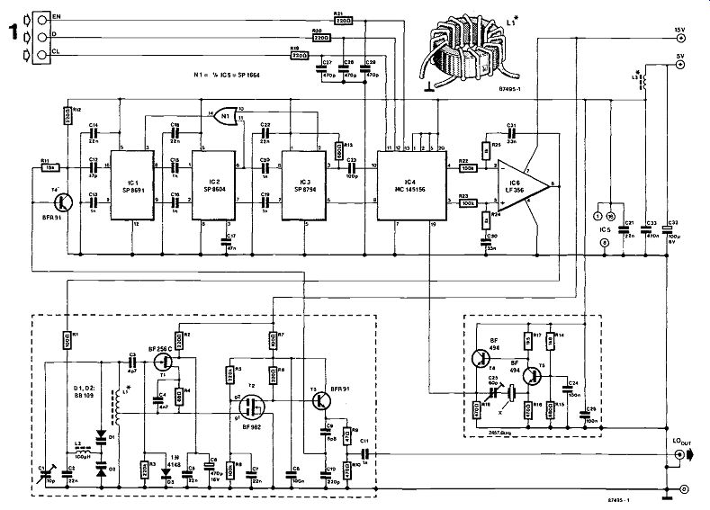
The synthesizer shown in Fig. 1 is computer con trolled, and outputs a local oscillator signal (LO) between 48 and 78 MHz for driving the mixer in the SW receiver proposed on page 00. The circuit is based on the Type MC145156 synthesizer from Motorola. This IC is relatively inexpensive, and ensures good LO suppression in the receiver when used in combination with a good mixer. Also of interest is its serial control input, which enables the output frequency to be Programmed from a computer.
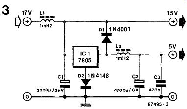
The internal reference frequency, 1200 Hz, is obtained by dividing the signal from oscillator T5-T6 by 2048. The DAC connected to the output of the first ID gives a resolution of 1200/255 5 Hz. The divider composed of IC,, IC2, ICs and Ni has a pre-scale factor of 128/129. Opamp IC6 is connected as a simple loop filter with a reference signal rejection of about 60 dB. An alternative filter that ensures a rejection of 80 dB, but has a slightly longer settling time, is shown in Fig. 2. This circuit is driven from the phase detector output of the synthesizer chip. Opamp IC1 is used in a speed-up circuit that may be included to equal the settling time of the filter with IC6. Diodes D1-D2 also serve to shorten the lock-in period of the synthesizer. The use of the Type E420 (Ti) is not obligatory: other types of AF double FET should also work in this application. The power supply for the synthesizer is shown in Fig. 3. The L-C filter in the + 5 V rail suppresses noise on the synthesizer supply, and D2 has been included to compensate for the drop across choke L2.
----------

-----------
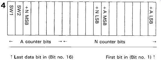
The data format for programming the MVC145156 is shown in Fig. 4. Bits SW, and SW2 control the switching outputs, and are not used here. The synthesizer divides by 128N + A: when counter A reaches state 127, N is increased by 1, and A becomes 0. Data is latched into the synthesizer on the trailing edge of the clock signal. When the control word is complete, the enable signal is briefly made high to transfer the data from the shift register to the programmable dividers. The squelch is then enabled to suppress locking and tuning noises.
The construction of this synthesizer requires some experience in building RF circuits. The ECL dividers and the synthesizer chip should lie upside down on an unetched board to enable effective grounding and cooling. The chips are interconnected with the shortest possible wires. Great care should be taken in the construction of the VCO and the TXO. These sections should be screened and built such that mechanical stability is ensured at all times. VCO inductor L1 is especially critical in this respect: make sure that the wire turns are secure on the core.
Finally, the winding data for the home-made inductors in this circuit: (use enameled copper wire): L1 (VCO): 14 turns 22SWG (0 0.8 mm) on a T50-12 core, tap at 4 turns from ground; L3 ( + 5 V rail): 8 turns 30 SWG (0 0.3 mm) through a ferrite bead.
163 TUNEABLE ACTIVE AERIAL FOR SW
Many of the modern, synthesizer-tuned, general coverage SW receivers incorporate the latest types of high dynamic range RF pre-stages and mixer devices, while the good old tunable preselector stage seems to have been eradicated in all but the most expensive and sophisticated types of multi-mode receiver. It would seem as if manufacturers associate a simple tuning control with an attack on user friendliness of the receiver, while a well-designed, tracked or individually controllable input attenuator would have been a better solution to the problems caused by the worldwide escalation of SW transmitter output levels.
A likewise argued plea for reestablishing the tuning control could be entered for the active aerial which, while not able to offer the performance of a long wire or multi-band beam aerial, is none the less generally recognized as a satisfactory means for receiving broadcast programs in the SW bands up to about 15 MHz.
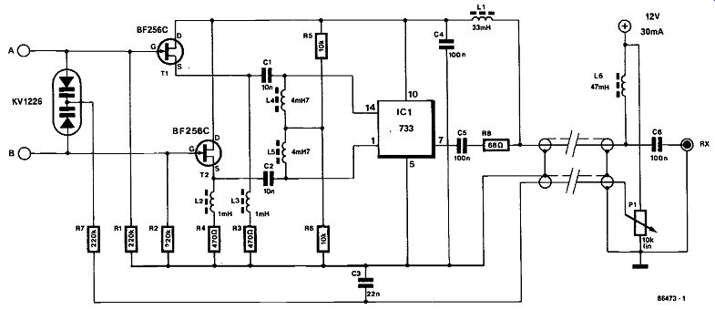
As generally known, an active aerial is composed of an aerial proper and associated amplifier. As to the latter, the circuit diagram shows that the design has a varactor-tuned, symmetrical input using two FETs Type BF256C which are fed over the coax cable to the receiver. Opamp IC, functions as a fast symmetrical to asymmetrical converter capable of operation up to about 30 MHz. Note that the varicap diode set is tuned over a separate cable; twin-lead 75 -ohm coax cable is, of course, ideal for the present purpose. The indicated varicap set ensures a tuning ratio of about 1:2 to 1:3.

------------
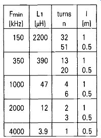
When constructing the aerial to this design, it should be noted that neither the circumference of the loop aerial nor the total length of the dipole must be in excess of one tenth of the relevant wavelength in order to ensure the correct directivity characteristics, especially in the case of the loop aerial; the dipole will typically fail to match the amplifier input impedance and thus cause problems in getting the device tuned properly.
Table 1 summarizes the aerial construction data, given a number of possible operating frequencies.
The aerial should be mounted in such a position as to receive a minimum amount of man-made, short range interference; the amplifier's symmetrical in put should ensure sufficient aerial directivity to find a dip for the interfering source.
The loop aerial is uncritical as to the height above ground, but not so the dipole, which is bound to act as a vertical rather than horizontal aerial when mounted at less than a quarter wavelength above ground.
Table 1.
164 TUNEABLE FM BOOSTER
-----------
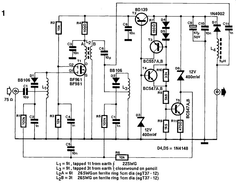
L1 = 9t , tapped 1t from earth { 22SWG
L3 = 9t , tapped 3t from earth closewound on pencil
L2A = 6t 26SWGon ferrite ring 1cm dia (eg T37- 12)
L2B = 3t 26SWG on ferrite ring 1cm dia (eg T37- 12)
This FM band (88-108 MHz) preamplifier has been designed to come round the problems associated with wideband as well as narrowband aerial boosters. Most commercially available boosters are wideband types with relatively poor selectivity and adjacent station rejection, while the (more expensive) narrowband types are rather impracticable when it comes to receiving stations well removed from the (fixed) frequency of peak amplification.
This proposed design is the best of both worlds, since it features good selectivity and strong signal handling, as well as a relatively low noise figure and sufficient amplification over the entire FM band.
Tuning the preamplifier is done in the living room, by means of a simple potentiometer mounted in an enclosure which is conveniently located next to the FM tuner as part of the hifi set.
The unit can also be made to function as a 2 meters amateur band (144-146 MHz) preamplifier by modifying the tuned circuits to suit the higher frequency.
The circuit diagram of the tuneable booster--Fig. 1--shows that two remote tuned circuits, along with a MOSFET tetrode have been incorporated to minimize the chances of running into cross- and/or intermodulation caused by strong local signals.
Varicap diodes D1 and D2 form the variable capacitance to coils L1 and L3 respectively. The tuned circuits are set to the desired frequency by means of the voltage applied to the varicap diodes (3 to 24 V, reverse bias). The RF gain offered by T1 should be of the order of 25 dB, while the noise figure is expected to be about 2 dB.

---------
The amplifier supply/tuning voltage and superimposed RF output signal are connected to the coax cable core which is run to the power supply/tuning unit, shown in Fig. 2. Tuning control potentiometer P1 constitutes the feedback loop to the voltage regulator composed of T7, T8 and T9. Turning Pi thus varies the voltage to the mast-mounted booster form 15 to 36 volts. Regulator T2-T3-T4 (Fig. 1) provides MOSFET T1 with a fixed voltage of 11.4 V, irrespective of the DC level on the coax core. Sub-
traction of 12 V from the 15-36 V input voltage is by means of zener D6 and current source Ts. RF output voltage and DC supply are coupled to the downlead cable through C1, and L4 respectively.
C14 and L5 (Fig. 2) have the same function in the PSU. D13 prevents the PSU output voltage from rising above 37 V in case of any breakdown in the supply unit, while D7 protects the booster from accepting a reverse voltage in case coax core and screen are accidentally reversed. T6 limits the supply short circuit current to a safe 60 mA.
The following are important points to observe in constructing the masthead amplifier and associated indoor control unit:
1. Use a copper-clad board of maximum earth plane surface (the Type 85000 RF prototyping board is ideal).
2. Mount a metal screen across the MOSFET case to suppress any tendency to parasitic oscillation.
3. Keep the source lead as short as possible; solder it direct to the copper surface.
4. Keep the leads of G2 decoupling capacitor C4 as short as possible; a ceramic disc capacitor is ideal for this purpose.
5. Keep all coil connections as short as possible to avoid amplifier tuning over the wrong frequency range.
6. Fit T9 with a small heatsink.
7. Mount a screen between amplifier and DC supply section.
After the construction of RF head and PSU has been completed, the latter is tested by verifying the presence of the variable (15.6 to 36.6 V) supply and tuning voltage on the coax cable core. The voltage across R14 should be lower than 0.4 V with the amplifier connected at the far end of the cable.
Turning P1 should cause the voltage at the collector of T5 to vary between 3 and 24 V.
The voltage at the emitter of T2 should be constant at 11.4 V with respect to ground, irrespective of the tuning voltage set with Pt Drain resistor R4 should drop between 0.7 and 2 V. Set P1 to the center of its travel.
Optimum RF performance of the booster can be achieved by carefully stretching or compressing L3 for maximum amplification at about 95 MHz; tune the receiver to a weak transmission at this frequency and align for maximum S meter deflection or optimum audibility of the signal above the noise level. Do the same for signals at either extreme end of the band and set Pi accordingly. Ensure that the tuning potentiometer can be set to give optimum amplification for every frequency in the 88 to 108 MHz band and mark the tuning scale on the in door unit in steps of 1 MHz. In case it is not possible to obtain equal amplification across the band, L3 may be adapted carefully by increasing or decreasing the number of turns. The tap, however, should remain at 3 turns from ground.
Those constructors striving for utmost perfection may fit a 40 pF trimmer capacitor instead of C1, in order that the amplifier may be tuned for optimum (i.e. lowest) noise figure, which is not the same as tuning for optimum amplification.
Finally, the coil data for the tuneable booster are as follows:
= 9 turns 22 SWG (0.7 mm dia) enameled wire, close wound, coil diameter 7 mm. Tap at 1 turn from ground.
L3 = the same, tap at 3 turns from earth.
L2a;L2b = 6 and 3 turns respectively, 26 SWG (0.5 mm dia) enameled copper wire on dia 10 mm ferrite ring Type T37-I2.
165 VLF CONVERTER
------------
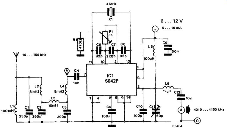
Strictly speaking, the VLF (very low frequency) band stretches from 3 kHz to 30 kHz, and the LF (low frequency) band, often called the long-wave band, from 30 kHz to 300 kHz. The converter de scribed here covers the frequency range 10 . .150 kHz and falls, therefore, half-way between being a VLF and an LF converter.
Frequencies between 10 kHz and 150 kHz are converted to 4.01. . . 4.15 MHz which can be fed to any short-wave receiver capable of accepting those frequencies. The converter is connected to the aerial input of the receiver via coaxial cable.
Many converters suffer from break-through of the mixer/oscillator frequency in the output signal, which is normally caused by the mixer being asymmetrical. Because of that, the present converter uses the well-known S042P frequency changer, the symmetry of which can be set accurately with a 1 k preset potentiometer connected between pins 10 and 12.
To prevent reception of image frequencies, the aerial signal is first applied to an LC band-pass filter, before it is fed to the frequency changer.
The output of the frequency changer (pin 2) is applied to an LC circuit that is tuned to the frequency range 4.01. . 4.15 MHz. This circuit, consisting of a 100 pH inductor in parallel with a 100 n capacitor and a 60 p trimmer, effectively suppresses any spurious signals produced in the frequency changer.
The 60 p trimmer is used to tune in to the desired transmitter in the 10 . . .150 kHz range (loudest reception!). The symmetry of the frequency changer is set by tuning the short-wave receiver to the frequency of the quartz oscillator, i.e., 4.00 MHz, and then adjusting the 1 k preset for minimum output from the converter, that is, minimum deflection of the S meter, or other field strength indicator, on the receiver. During this calibration, the input of the frequency changer, point A in the diagram, should be short-circuited to earth.
All inductors are standard RF chokes. The value of the output inductor, 121.4H, is not critical.
The aerial should be as long a wire as possible.
166 WEATHER SATELLITE INTERFACE

------------
An increasing number of electronics enthusiasts is becoming interested in weather satellite reception.
Most non-geostationary weather satellites, like those in the NOAA series, operate in the 138 MHz carrier. For optimum reception, the detector should feature a relatively high carrier suppression.
It is assumed here that a picture signal is available on a cassette tape. Opamp Ai has an amplification of 48, while A2-A3 form a precision two-phase rectifier. The 2,400 Hz ripple arising from the slightly different specification of the opamps amounts to no more than 0.2%. For commonly used A-D converters, this corresponds to an error smaller than 1/2 (LSB).
The main ripple signal is 4,800 Hz. This is readily removed by a double 71 filter set up around L1 and L2. At 2500 Hz, the attenuation is about 3 dB, at 4,500 Hz about 45 dB. The parallel R-C and L-C networks at the + input of As compensate for the ohmic resistance of the inductors in the pi filter. L1, L2 and L3 are preferably ferrite-encapsulated chokes from the Toko 10RB series, available from Cirkit PLC (L1 & L2: 181LY-473. L3: 181LY-104).
The interface is suitable for processing carrier frequencies up to 4,800 Hz, so that it is possible to play the tape at double speed for reading into the computer (provided, of course, the program can handle this). Components RH, D4 and Ds protect the A-D converter against voltages higher than 5 and lower than 0 volt. The use of the Type CA3130 Bi-Mos opamp ensures an output voltage swing of 5 V when a ±6 V supply is used. The maximum supply level and current consumption are ± 9 V and 15 mA respectively. The input signal amplitude should be greater than 68 mV_rms for a 5 Vpp output.
---------