237 12-VOLT NI-CD BATTERY CHARGER
If you attempt to charge a 12 V Ni-Cd battery from a 12 V lead-acid car battery, you will soon find that that is not really possible: the charging voltage should be somewhat higher than the nominal battery voltage. A 12 V battery should be charged from a source of about 14 V.
The present circuit is, therefore, a voltage doubler based on the well-known 555 IC. The IC oscillates, which means that output 3 is connected alternately with earth and the +12 V supply voltage.
When pin 3 is logic low, C3 is charged via D2 and D3 to almost 12 V. When pin 3 is logic high, the voltage at the junction of C3 and D3 becomes almost 24 V, because the negative terminal of C3 is at + 12 V and the capacitor itself is charged to about 12 V. Diode D3 is then reverse biased, but D4 conducts, so that C4 is charged to just over 20 V, which is ample for our purposes.
The 78L05 in the IC2 position functions as a current source, which tends to keep its output voltage, Uri, appearing across R3, at 5 V. The output current, in, is therefore easily calculated from Irl = Un/R3= 5/680 = 7.4 mA.
The 78L05 itself also draws current: the central terminal (normally earthed) delivers about 3 mA. The total load current is, therefore, of the order of 10 mA, which is a good value for continuously charging NiCd batteries. The LED has been incorporated to indicate that charging current flows.
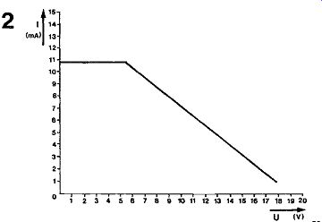
The characteristic of the charging current versus battery voltage in figure 2 shows that the circuit is not perfect: a 12 V battery will be charged with a current of only about 5 mA. There are several causes for this:
-- the output voltage of the circuit tends to drop with increasing current;
-- the voltage drop across the 78L05 is about 5 V to which must be added the 2.5 V the IC needs to operate correctly;
II there is a voltage drop of about 1.5 V across the LED.
None the less, a 12 V NiCd battery with a rated capacity of 500 mAh can be charged continuously with a current of 5 mA, which is 1 percent of its capacity.

--------
--------
238 ACTIVE RECTIFIER WITHOUT DIODES
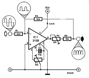
The active rectifier proposed here is based on the property of an operational amplifier that its output cannot become negative if its power supply is asymmetrical. We have used an RCA type CA 3130 opamp which is eminently suitable, because it can cope with input voltages down to 0 V, and has a CMOS output stage that can also work down to 0V.
With a supply voltage of 15 V, the maximum input level is about 1.2 V_rms. The frequency range, for not more than 1 dB change in output, extends from DC to just over 25 kHz.
Negative half cycles at the input of the opamp are inverted and amplified by a factor R2/R1. Positive half cycles are also inverted, but, as stated, the output of the opamp cannot become negative, and it therefore remains at 0 V. The positive half cycles are also applied to the output of the opamp via a resistive divider, R1-R2-R3-P2 The result of all this is that only positive half cycles are present at the output, just as if full-wave rectification had taken place. If the asymmetry of the supply is set correctly with Pg the peak values of the inverted negative half cycles and the positive half cycles are equal.
Preset D1 should be adjusted to give zero output when the input of the opamp is connected to earth.
The rectifier has a low-impedance input (source impedance should be not greater than 100 ohm) and a high-impedance output (load impedance should be not less than 1 M-ohm). If these requirements as to source and load impedance cannot be met, the values of R1 and/or R3 should be modified: R1 + source impedance should be about 2k2, while the parallel combination of R3 and the load must be around 10 k-Ohm.
----------
239 BATTERY CHARGE/DISCHARGE INDICATOR
Many of today's cars and motorcycles are equipped with a meter for monitoring the battery voltage.
However, this meter does not provide information on the battery condition, or whether it is being charged at all. When the voltmeter reading is too low, the battery is generally in such a poor state as to necessitate switching off heavy loads to save power for use of the starter engine later. Especially on motorcycles, the battery capacity is relatively low, which justifies the need for a reliable monitoring system. A standard 30 A ammeter offers too low resolution, and is rather awkward to fit permanently.
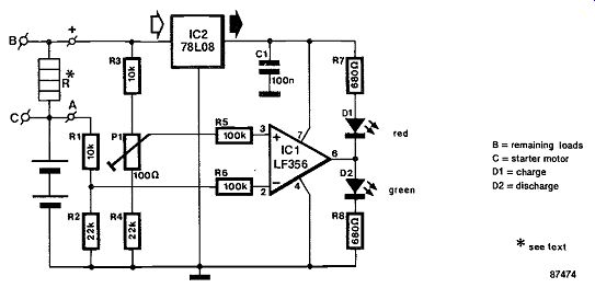
In this charge/discharge indicator, the measured current is converted into a potential difference by R., which is either two 1R0 5 W resistors, a fuse, or a few turns of copper wire. The direction of the current through R. is detected by comparator IC t, which then indicates whether the battery is being charged or discharged by lighting the relevant LED.
The 100R preset enables shifting the indication threshold somewhat. Input terminal + on the indicator unit is best connected to a point behind (that is, electrically behind) the contact switch, although it is also possible to fit the circuit with a separate on/off switch. Finally, the circuit is only suitable for use in or on vehicles having a 12 V battery.
------
B = remaining loads C = starter motor
D1 = charge
D2 = discharge
87474
240 BATTERY CHARGING INDICATOR
Sealed 6 V or 12 V lead-acid batteries, under normal charging conditions, are charged at a constant voltage of 2.3 V per cell. The charging current reduces during the charging: when it reaches a value of 10 mA, the battery is deemed fully charged. To check this, you do not need an expensive ammeter. The present circuit uses an LED (light-emitting diode) to indicate when the battery is fully charged.
The green indicator LED is connected in the collector circuit of a p-n-p transistor. As soon as the transistor conducts, the LED lights. This happens when the voltage drop across resistor R1 reaches the for ward bias threshold of the base emitter junction (about 0.6 V). When this resistor has a value of 56 ohm, a charging current of around 10 mA will cause this drop. To ensure that the charging current can exceed 10 mA, R1 is shunted by diode D1 which limits the voltage drop across the resistor to about 0.7 V. The maximum charging current depends on the diode used and lies between 1 and 3 A.
The LED does not light when the charging current is less than about 10 mA, i.e., when the battery is fully charged, when the battery is connected with wrong polarity, or when the output is short circuited. The red LED will light when the battery is connected with reverse polarity.
The indicator should be connected between the charger and the battery. It may either be built into the charger housing, or be constructed in a small case that can conveniently become part of the charging cable.

----------
241 BATTERY FITNESS CENTER
This circuit is designed primarily for maintaining lead-acid batteries that are often not used for long periods in good working order. It charges the battery, after which the battery discharges slowly through its internal resistance and the present circuit. When the state of charge reaches a predetermined level, the charger is switched on again, the battery charges, and so the cycle repeats itself.
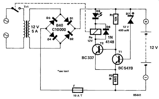
The circuit is based on Schmitt trigger T1/T2. Zener diode D7 determines the state of charge at which the charger is switched off. Resistor R2 provides the required hysteresis. With the mains disconnected and no battery connected to the battery terminals, check with voltages (from a regulated power supply) of 13.6 V and 12.5 V applied across the battery terminals that the relay switches off and on respectively. The "on" threshold may be corrected by, for instance, connecting a 1N4148 (cathode to + line!) in series with D7. The "off" threshold is corrected by altering the value of R2, for example, by replacing this component with a 100 ohm preset.
It is, of course, possible to replace the mains transformer and bridge rectifier by a battery charger (see, for instance, Elektor Electronics, June 1984, p. 6 45), in which case the rest of the circuit can be fitted inside the charger.
It is not possible to connect a full discharged battery to the circuit, because the relay would not be energized. Such a battery should first be charged to above 10V, but it is also possible to fit a switch in parallel with the relay contact and switch on the mains with that.
It is possible, of course, to maintain two 12V batteries in condition by doubling the secondary voltage of the mains transformer, the zener voltage of D7, the hysteresis, the rated coil voltage, and connecting the batteries in series across the terminals.
Fuse F1 is necessary to provide protection against short circuits. The transformer primary circuit may also be protected by a fuse (like F1 a delayed action type) rated at 1A.
The circuit does not need a smoothing capacitor because that function is carried out by the battery.
---------
242 BATTERY GUARD
This protective circuit is readily incorporated in battery-powered equipment which is typically in tended to operate for less than about a minute; possible applications that come to mind include IR remote control units, calculators, etc. Forgetting to switch off such devices irrevocably causes the built in batteries to be exhausted after a while, however "low" the standby current.
The proposed battery guard automatically switches off the supply current to the circuit, either after about one minute has lapsed after power-on, or when the battery voltage has fallen below the acceptable level for normal operation.
Series regulator FET T1 can pass a maximum current of 150 mA in the circuit as shown, and it is advisable to use a more powerful type than the BS250 in case more than about 100 mA is expected to be consumed by the equipment connected to the output terminals. The Type BS250 FET drops about 0.5 V at a drain current of 100 mA, and 0.8 V at 150 mA, whence the foregoing consideration.
As T1 is a p-channel FET, it conducts and powers the equipment when the output of Schmitt trigger NAND gate N3 is low, i.e. when both gate inputs are high. This is so at power-up, since C2 is still discharged and the inputs of N4 are kept at logic low level via R6. Consequently, T1 is enabled and causes C2 to be charged via R3. After about one minute (R-C time), the voltage across R3 is low enough for N3 to recognize a logic low level at pin 1, thereby turning off T1. N2 provides a hold function of this state, since otherwise N3 might oscillate owing to the slowly varying voltage across R3.
At power-on, the output of N2 is pulsed high by means of R-C network R1-R2-C1, whereby any residual charge in C2 is cleared; the circuit may, therefore, be switched on with S2-S1 immediately after automatic power down.
Battery voltage monitoring is accomplished by D3, R5, Re and N4. The latter's trigger threshold level is, as with all Schmitt trigger gates, in direct proportion with the supply voltage level to the IC. As long as the supply (i.e. battery) voltage is sufficiently high, N4 will recognize a logic low level at junction R5-Re-N4. However, if the battery voltage falls, D3 keeps the input voltage to N4 at a fixed level, causing the gate to supply a logic low level to N3, which consequently turns off the series regulator FET.
It should be noted that the exact values of R3, C2, R5 and R6 may have to be adapted to suit operation with certain makes of the Type 4093. Also note that the interval time of one minute may be changed to individual requirements by suitable re-dimensioning of timing elements R3-C2.
Adjustment of the battery guard is carried out by temporarily exchanging R5 and R6 with a 100 k preset to determine the correct resistor values for a given switch-off level. Current consumption of the proposed circuit is mainly determined by the zener diode, which has been biased to pass only 1 mA.
After automatic power-down, the guard circuit draws a (negligible) current of less than 1 µA.

-------

------------
243 CURRENT INDICATOR
Who has not sometimes wished that the power supply he was using had a voltmeter AND an am meter? Unfortunately, the high cost of such units prohibits their use in many situations. The proposed circuit, which does not include the input section of the power supply, can be built from standard components, except for the low-value 5-watt resistors.
We shall not dwell on the well-known Type L200 voltage regulator, but shall confine ourselves to the current indicator section.
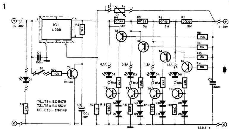
Fig. 1 shows that the circuit contains five LEDs: one (131) to show whether the supply is switched on, and the other four to indicate the current consumption in steps of 0.5 A; 0.8 A; 1.3 A; and 1.8 A. As may be deduced from these figures, the unit is capable of providing up to 2 A at an output voltage anywhere between 3 V and 30 V. The color of the LEDs is immaterial, although it would be useful if the final one would be red to show that maximum current is being drawn.
The non-standard resistors, R4 to R7 incl., "measure" the actual current consumption. between point A and the positive output terminal there exists a potential difference. When this p.d. reaches a value of 0.6 V, T2, and consequently Ts, switch on and this causes D2 to light. In the same way, when the p.d. between points B, C, and D respectively, and the positive output terminal reaches about 0.6 V, transistor pairs T3-T7; T4-T8; and Ts-Ts switch on, and the associated LED will light.
Resistor R2 and capacitor C2 provide a soft start facility at switch-on. Transistor T1 provides an emergency switch-off facility, which in practice has proved very useful.
The input section (not shown) should consist of a mains transformer with 24 V; 2.8 A secondary; a bridge rectifier (e.g. B80C2200/3300); and a 4700 uF; 40 V smoothing capacitor.
The L200 regulator should be mounted on a suitable heat sink. This device has internal short circuit and overload protection; its pin assignment is given in Fig. 2.
1 = input 2 = limiting circuit 3 = ground 4 = reference voltage 5 = output 6 = ground 86448-2
--------

--------
244 CURRENT INDICATOR FOR 723
Although the Type 723 voltage regulator has been with us for quite a few years, it is still a favorite component for making simple and good quality power supplies. The 723 possesses excellent characteristics, including a highly stable output voltage, adjustable current control, and short-circuit protection, but it lacks an output for signaling the activity of the built-in current limiter.
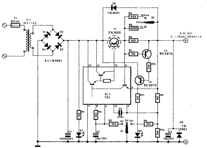
The current limiter in the 723 consists of only one transistor, whose base and emitter are brought out to chip pins 2 and 3 respectively. When the voltage across these pins exceeds 0.5 to 0.6 V, the transistor is turned on and cuts the drive to the output transistors. In most applications, the voltage drop for the B-E junction of the current sense transistor is developed across an externally fitted resistor. In the supply proposed here, this is either Rs, Rd/Rs, or Rd/Rs. A difficulty arises if it is intended to provide an overcurrent indication for the shutdown circuit with the aid of an external transistor fitted in parallel onto pins 2 and 3, since the external and internal transistor are highly unlikely to have precisely the same characteristics. When the internal transistor has the low B-E voltage of the two, the indication will not work, while in the other case the external transistor takes away the base current for the internal transistor, so that the current limiter is rendered ineffective.
In this design of a power supply, a current overload indication was realized by fitting the external transistor with a high value base resistor, R7, to ensure that the current limiter in the 723 is not disabled.
A further transistor, T3, has been added to keep the base current for T2 as low as possible. Since the base-emitter junction then has a diode characteristic, the associated voltage drop is always lower than that of the transistor internal to the 723.
The three output voltages from this supply are probably the most commonly used for testing asymmetrically fed designs: 5 volt for many TTL and CMOS circuits, 9 volt for battery operated equipment or logic circuits equipped with a 7805 regulator (this requires an input of at least 8.5 V), and 12 volt for RS232 drivers, and miscellaneous opamp or transistor based circuits.
The current limiter can be set to 10 mA, 100 mA, or 1 A for safely powering experimental circuits.
Power regulator T1 should be fitted with a heat sink sized at least 10 x 10 cm. LEDs D7 (green) and Ds (red) are the power on and current overload indicator, respectively.
The output voltages of the supply may not be as ac curate as required, and this is mainly due to the use of resistors from the E12 series. Close tolerance is especially important in the 5 V range, since the value shown for R3 gives a theoretical output of 4.9 V. This can be increased readily by fitting a resistor in parallel with R3, until the output voltage is 5.0 V precisely. Switches S1 and S2 are preferably SPDT types with a center position, but three-way rotary switches should also do if in both cases the center contact is not used.
------------
245 DC/DC CONVERTER
In circuits where two signal paths must be electrically isolated, use is often made of an opto coupler. Unfortunately, these devices require two power supplies: one for the sender, and the other for the receiver. In industrial and professional under takings this requirement is met by a proprietary DC/DC converter. As these are by and large very expensive, they are not of very much interest to the average hobbyist. However, the do-it-yourself converter presented here is much less expensive and, moreover, easy to build.
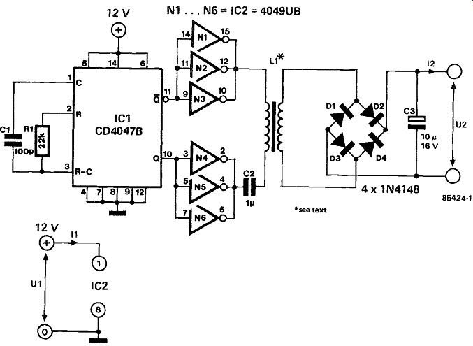
The circuit diagram in figure 1 shows that the converter consists of an oscillator, IC), and a driver, IC2, on the primary side, and of a rectifier, D1 . . D4, and buffer capacitor, C3, at the secondary.
In our prototype, operating from a 12 V battery at the maximum 74 percent efficiency, we measured a secondary output voltage of 10.64 V, and a secondary output current of 9 mA (the corresponding primary current amounted to 10.8 mA). The secondary current should not exceed 10 mA, because the secondary output voltage then drops below 10 V and the efficiency deteriorates. That applies also to low-load conditions: when the secondary is open-circuit, the output voltage is 14 V, but the efficiency is, of course, 0 percent! In other words: the circuit works optimally at a secondary load current of 9 mA.
Oscillator IC, operates at a frequency of around 100 kHz. Its two output signals are each amplified in three parallel-connected buffers contained in IC2, and then applied to the primary of the isolating transformer. The voltage induced in the secondary winding is rectified and smoothed by C3. The stated value of that capacitor is more than adequate for the relatively high secondary frequency of 200 kHz.
The isolating transformer is a DIY item: it is wound on a pot core of 22 mm dia. and 13 mm high with 0.35 mm dia. enameled copper wire- 80 turns for the primary and 80 turns for the secondary. The specific inductance, AL, of the core should be 400 nH. The core should not have an air gap. Insulating foil should be placed between the two win dings to ensure an isolating voltage of 4 kV.
------------
246 DIGITAL VOLTAGE/CURRENT DISPLAY
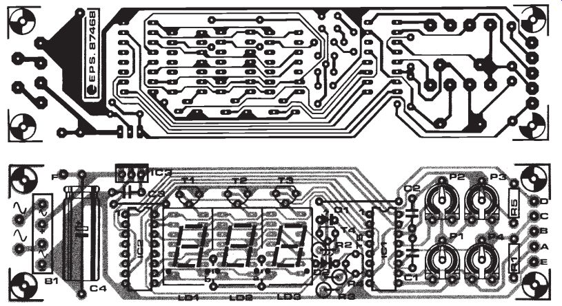
This VII display module is eminently suitable for building into an existing DC power supply, where it gives a precise indication of the set voltage or the current consumption of the load.
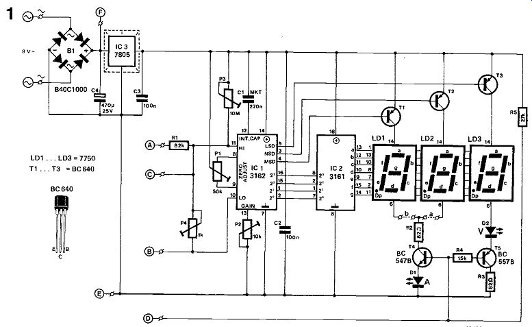
The circuit diagram appears in Fig. 1. The 3-digit readout is based on A/D converter Type CA3162 and BCD-to-7 segment decoder Type CA3161, both from RCA. The common anode connections of LED displays LD1-LD3 are successively connected to the positive supply line via T,
Provision has been made to select the correct position of the decimal point. In the voltage range, the decimal point lights on LD3, and the resolution is therefore 100 mV. Two current ranges are possible: 0-9.99 A (link a) or 0-0.999 (.999) A (link b).
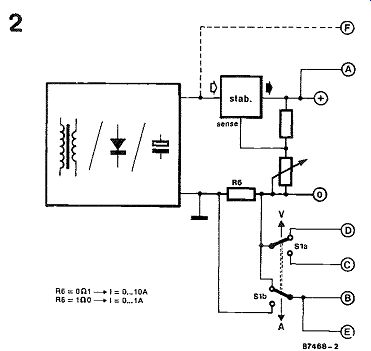
The current sensing resistor is therefore either 0R1 or 1-R-0--see Fig. 2. It is important that R6 does not affect the output voltage of the supply in question. It must, therefore, be fitted ahead of the voltage divider that controls the output voltage. DPDT switch S1 selects between voltage and current readings.
When voltage measurement is selected, P4-R1 attenuates the input voltage by a factor 100. Also, point D is pulled low so that the decimal point on the IS display, and the "V" LED, are illuminated.
When current measurement is selected, the drop across the sensing resistor is applied direct to the HI-LO inputs of DAC IC). The sensing resistor has such a low value as to render the voltage divider in effective.
There are four adjustment points in the module:
P1: current range nulling;
P2: full-scale current calibration;
P3: voltage range nulling;
P4: full-scale voltage calibration.
-------------
-------------
These points should be adjusted in the above order.
Two presets, Pi and P3, are required to ensure correct nulling of the module. P1 compensates for the quiescent current consumption of the regulator circuit in the supply. The resulting small negative deviation in the voltage range is compensated by P3.
The VII display module is conveniently fed from the unregulated voltage available in the supply (max. 35 V)-see points E and F in Fig. 2; bridge rectifier B1 may then be omitted. The minimum in put voltage for IC3 is 8 V, and this regulator should be fitted with a heat-sink if the input voltage is greater than 12 V. It is, of course, also possible to power the module from a separate 8 V; 200 mA mains transformer.
The unit can be constructed as a double to obtain simultaneous V and I readings. It should be noted, however, that the current sensing resistor is short-circuited via the ground connections when both modules are fed from the same supply. There are two ways to overcome this problem. One is to feed the V unit from a separate supply, and the I unit from the "host" supply. The other is more elegant and entails hard wiring points E to the left side of the current sensing resistor. Note, however, that the highest V indication then becomes 20.0 V (Rs drops 1 V max.), since the voltage at pin 11 may not exceed 1.2 V. Higher voltages can be displayed by selecting the lower current resolution, i.e., R6 becomes 0R1. Example: R6 drops 0.5 Vat a current consumption of 5 A, so that 1.2-0.5 = 0.7 V re mains for the voltage indication, whose maximum reading is then 100 x 0.7 = 70 V. Again, these complications only arise when two of these modules are used in a single supply.
Parts list
Resistors ( ± 5%):
R1 =82K
R2;R3 = 82R
R4 = 15K
R5 = 27K
R6 = 0R1 or 1R0*
P1 = 50K preset
P2 = 10K preset
P3 = 10M preset
P4 = 1K0 preset
Capacitors:
C1 =270n
C2;C3 = 100n
C4 = 470 II ;25 V
Semiconductors:
D1; D2 = LED red B1 = BC40C1000 LDi;LD2;LID3=7750
. . .T3 incl. =BC640 T4 = BC547B T5 = BC557B IC, =CA3162 IC2=CA3161 IC3=7805
Miscellaneous:
S1 = miniature DPDT switch.
PCB Type 87468 " See text.
-------------
247 DIRECT-CURRENT MONITOR
Many direct-current monitor circuits use a resistor in series with the current-carrying wires, and actuate some indicator by the ensuing voltage drop across that resistor. The drop causes a reduction in the available load voltage, which at relatively high currents can be appreciable. In the present circuit, use is made of a reed relay, around which the current-carrying wire is wound a number of times.
The consequent losses are minimal. This method has a bonus in that a switch contact is immediately available for a number of applications.
One possible application is that of a low loss lamp monitor. As long as the lamp (here represented by RL) is on, the LED lights. The number of turns depends on the relay use;., and the load current. As a guide, most reed relays operate at 50 ampere-turns, so that in the case of, say, a car headlight (60 W at 12 V gives a current of 5 A) about 10 turns are required.
The more complex circuit diagram shows an electronic fuse, which also offers overvoltage protection.
The state of the circuit is indicated by two LEDs.
When the supply is switched on, the thyristor is off, and relay Re will be energized via the 150-ohm resistor. The load will then be connected and the green LED lights.
If the load current becomes too high, the reed relay will close and trigger the thyristor via the 470-ohm resistor. The thyristor then short-circuits relay Re, which causes the load to be disconnected. At the same time, the green LED will go out and the red one will light. The circuit may be reset with S2, which breaks the current through the thyristor and causes it to switch off.
Overvoltage protection is provided by the zener diode across the reed relay. When the input voltage becomes greater than the zener voltage and the thyristor trigger voltage, the thyristor will be triggered and switch on the protection circuit.
These two applications are primarily of use in cars, but, no doubt, ingenious readers will think of others.

-----------
248 DIRECT-VOLTAGE DOUBLER
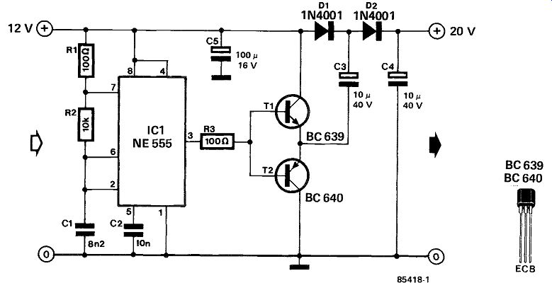
A direct-voltage doubler is particularly useful when from an available supply voltage a higher one has to be derived. As the current in most such cases is pretty small, the cost of a suitable circuit can be kept down.
-------------
Astable multivibrator IC, is a rectangular-wave generator operating at about 8.5 kHz whose output drives transistors T1 and T2 When the level at pin 3 of IC, is low, T1 is off and T2 conducts. As the negative terminal of C3 is then connected to earth, the capacitor charges via diode D1. When the output of IC, is high, T2 is off and T1 conducts. Capacitor C3 cannot discharge because of D1, but C4 charges to a voltage roughly equivalent to the supply voltage of +12 V and the p.d. across C3 and Di. In our prototype, this voltage across C4 amounted to 20 V approximately. The maximum current should not exceed 70 mA: at that value, the output voltage is 18 V, at an efficiency of thirty-two percent.
We have not tested the circuit with other supply voltages, but it can be safely assumed that it can be used over the whole supply voltage range of the NE 555.
Construction is possible on a small piece of prototyping board, after which the doubler can be fit ted inside the power supply unit.
If a regulated output is required, it is possible to connect an appropriate voltage regulator, for in stance, in the 78LXX series, but in that case the power requirements of the regulator must, of course, be taken into consideration when the maximum load current is calculated.
249 ECONOMICAL POWER SUPPLY
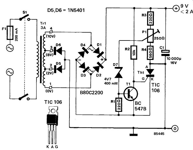
The power supply described here uses a silicon-controlled rectifier (SCR) that, depending on the load current, selects taps on the secondary of the mains transformer. The output voltage of around 9 V is eminently suitable as input voltage for a 5 V regulator, which consequently works with the absolutely minimum power dissipation.
With low to medium load currents, the SCR is in the blocking state. Rectification of the secondary transformer voltage then takes place in D1, D2, D5, and D6 only. The load current flows during the positive half cycle via D1, load, and D5; during the negative half wave it flows through D2, load, and D6. The tapped secondary voltage amounts to 8V in either case, while a 2V section remains unused.
With increasing load current, the output voltage drops until no current flows any more through the zener diode. Transistor T7 switches off which removes the short circuit from the gate of the SCR, which then conducts. As soon as that happens, the full secondary transformer voltage is rectified by D1 . D4, while diodes D5 and D6 are reverse biased.
---------------
As the voltage across the zener diode is always lowest during the zero crossing of the secondary voltage, the SCR always switches on at or near that instant. This prevents high current pulses and other noise often associated with SCR switching: no further suppressors are therefore necessary.
To build this supply, you need a mains transformer with a 12 V secondary that has taps at 2 V steps:
2-4-6-8-10-12 V. For load currents up to 1.5 A, a 2 A transformer will suffice; an output current of up to 2 A requires a 3 A transformer.
250 LEAD-ACID BA1TERY CHARGER
Although in electronics more NiCd than PbH2SO4 batteries are used (or so we're told), there is still a healthy demand for good chargers for the lead-acid types. The present one enables 6- or 12-volt types to be charged rapidly; switches itself off automatically; and is protected against thermal overload, short circuits, and polarity reversal of the battery.
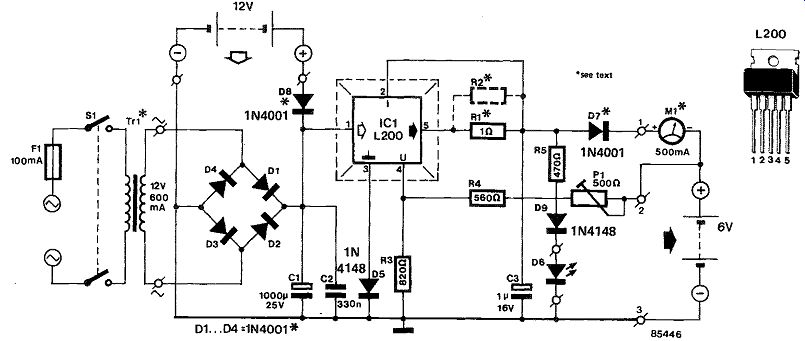
If you are not fully acquainted with modern sealed lead-acid batteries, here are some of its more important properties. It may be used in any position, even upside down. The charging voltage should be 2.3 V per cell (2.45 V for fast charging): i.e., 6.9 V for a 6 V battery and 13.8 V for 12 V types. The charging current need not be limited to 0.1 . . .1 C ( = capacity in Ah- the actual figure depends on the manufacturer). The battery is charged when the charging current has dropped to 1 percent of the capacity. Some manufacturers state that it is preferable that their batteries are charged in a horizontal position. Never charge these batteries with a NiCd battery charger!! The circuit of the suggested charger is based on a type L200 voltage regulator which ensures a constant charging voltage. The actual level of the charging voltage is set with D1 in the absence of a battery.
Resistors R and R2 provide current limiting, but R2 is only necessary if a charging current above 0.5 A is required or to enable the output current more precisely. The current is limited to [0.45(R, +R2)1R1R2] A; its actual value is indicated by M1.
Table 1.

-------
The L200 may be mounted on a small heat sink, but this is not strictly necessary since the device has internal thermal protection.
Normally, the battery charger works from the mains, but it can also operate from a 12 V (car) battery.
All possible situations, some of which are highly undesirable, are enumerated in table 1. The one exception is that when the battery is really flat, the table does not apply. The battery must then be seen to be connected correctly to the charging terminals. Also, the LED indication will then initially not work.
Table 2 gives some examples of 6 V batteries and circuit variations required for the different types.
The charging currents here are limited to 1/10 of the battery capacity in Ah (ampere-hours): this is a safe value which is permissible under all circumstances).
If the charger is required for n V batteries, the mains transformer must have a secondary voltage of at least 18 V, and capacitor C1 must become a 35 V type. Furthermore, resistor R4 should be increased to 1k8 and preset 131 to 1 k-Ohm.
Table 2.
Parts list
Resistors:
= 1 g R2 = see text
R3 = 820 g
R4 = 560 g (see text)
R5 = 470 ohm
= 500 ohm preset (see text)
Capacitors:
C, = 1000 m/25 V (see C2 = 330 n C3 = 1 µ/16 V
Semiconductors:
D1 ... D4,D7,D6 =
(see table 2) D5,D9 = 1N4148
D6 = LED
IC, = L200 text) 154001
Miscellaneous:
M1 = moving coil meter, 500 mA f.s.d.
Tr1 = mains transformer, secondary 12 V, 600 mA (see text)
S1 = DPST mains on/off switch
= fuse, 100 mA, delayed action heat sink for IC, (optional- see text)
PCB 85446

----------
251 LOSS-FREE SUPPLY PROTECTOR
Any diode-based circuit that protects against reversal of the supply polarity introduces a certain voltage drop. Also, when relatively high currents are involved, the choice of a suitable diode, and its dissipation, may become problematic.
This circuit utilizes a relay contact to break the positive supply line when the input voltage has the wrong polarity. The coil voltage of the relay may be lower than the input voltage, because Re is activated within a few milliseconds, and then receives the correct coil voltage via T1-P1. Since the hold voltage of a relay is generally lower than the actuation voltage, D2 can be dimensioned such that the relay operates reliably with a minimum of zener current taken from the supply.

--------
252 LOW-DROP VOLTAGE REGULATOR
Integrated 3-pin voltage regulators are not suitable for use where the input and output voltages are nearly equal. In fact, with most such regulators, the input voltage is typically 3 V higher than the output potential. To cater for situations where the two voltages are nearly equal, it is necessary to use discrete components. The series transistor is then connected in a common emitter circuit, so that the output voltage is lower than the input voltage only by the saturation voltage of the transistor. However, it is then difficult to provide short-circuit protection as is the case in integrated regulators. But, where there is a will, there is a way.
In Fig. 1, the series transistor obtains its base current from T2, which together with T1 forms a differential amplifier. This arrangement ensures that the junction of voltage divider Ra-Rs has the same potential as the cathode of zener Dz. The crux of the circuit is that T3 has a certain current amplification, but 12 can only provide it with as much base current as R2 allows. The potential difference across R2 has a maximum value of the zener voltage minus the base-emitter voltage, UBE, of T2, which in practice is about 4 V. The maximum current through R2 is, therefore, about 11 mA, so that, assuming that T3 has a current amplification of 50, the maximum output current is 0.55 A. If a higher current is drawn, the output voltage will drop. If it drops below the zener voltage of D2, the p.d. across R2 will drop also. The result is that the output current will behave as shown by the fold-back characteristic in Fig. 2. It is clear, therefore, that the series transistor is protected against high (short-circuit) currents.
Diode D1 and resistor R: provide a soft start, because the voltage across the diode, which is connected to the output of the regulator, is zero at switch-on. Since the circuit, because of the high gain, has a tendency to oscillate, capacitor C: is included to improve the stability.
The output voltage level, U0, can be freely selected, within the limits of the series transistor, by D2, R3, and R4, and is determined from Uo = Uz(Rs + R4)/Rs.
Resistor R2 must be matched with the actual current amplification of the transistor used. The maximum dissipation of a well-cooled BD140 is of the order of 5 W. If a noise-free output is required, an additional 10µF electrolytic capacitor should be connected in parallel with Dz. The circuit will then have a real soft start: there will be no output for about 0.2 s after switch-on.
-----------

253 MAINS POWER SUPPLY WITH PRIMARY REGULATION
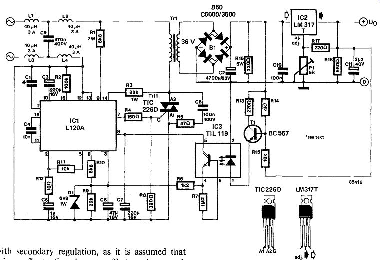
The unusual circuit shown in figure 1 has an unusual efficiency: according to SGS, this amounts to no less than 37 percent at an output voltage of 3 V and output current of 2 A. With traditional secondary regulation, an efficiency of about 8 percent would have been normal. The output voltage can be varied over the range 1.2 . . .25 V, and the output current can be 1.5 A at any of these voltages, provided IC2 is mounted on a suitable heat sink.
Another advantage of primary regulation is that the power supply is protected against variations in the mains supply. This aspect is normally ignored with secondary regulation, as it is assumed that primary fluctuations have no effect on the secondary regulation. The present circuit is, therefore, of particular importance for use where the mains supply is subject to large variations.
The regulation functions so that the voltage drop across voltage regulator IC2 is held constant. This voltage drop is transferred by current source T1 into a current through the LED in the opto-coupler.
When the voltage drop diminishes, the current through the LED is smaller. The transistor in the opto-coupler gets less drive, and the voltage at pin 3 of IC, drops. Voltage regulator IC, contains a complete circuit for phase gating control with silicon- controlled rectifier Tri1. The gating angle of this triac depends on the comparison between the direct voltage at pin 3 and an on-chip generated sawtooth signal, the frequency of which is determined by capacitor C1 ( = 100 n). In our example, the triac switches the mains voltage earlier so that buffer capacitor C2 receives more energy.
Noise caused by the phase gating circuit must be prevented of entering the mains supply by a mains noise filter as shown.
SGS application
------------
254 MAINS ZERO-CROSSING DETECTOR
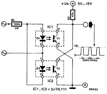
Both safe and remarkably simple to construct, this circuit detects the zero crossing moments of the mains voltage, in order to provide other circuitry with timing information about the correct instant for switching mains-connected loads; in other words, when the least possible switching dissipation is involved, and, therefore, least interference is induced on the mains lines.
The proposed circuit operates direct off the mains, while comprising no more than two opto-couplers and two resistors. It is seen that photodiodes D1 and D2 are connected in antiparallel while being fed with the mains voltage via a resistor, which limits the current through the relevant diode to about 2 mA as it conducts (i.e. lights) during the negative or the positive half wave (D2 or D1 respectively) of the mains sinewave; in either case, the circuit output voltage is low, since the associated phototransistor conducts and draws current from + Ub via R2.
However, at the moment of zero crossing, neither one of the diodes conducts, and the voltage at the circuit output rises to near + Ub level, whence the 100 Hz pulse train.
The value of R2 may be adapted to suit the level of + Ub and the manufacturer-specified typical collector current through the phototransistor. For the Type TIL111, the current should not exceed about 50 mA. The type of optocoupler used in the circuit should not be very critical, but the value of RI had best be left at the indicated 100 k so as not to run into excessive diode dissipation.
-----------
255 NEGATIVE SUPPLY CONVERTER
It is sometimes required in certain circuits that are powered from just one battery to derive a negative supply voltage from the positive battery potential.
As the loading of such negative lines is normally pretty minimal, it is possible to use a TL 497A IC to provide the negative voltage. This saves a trans former, rectifier, and a smoothing capacitor.
The TL 497A is a switch-mode IC from Texas Instruments, that may be used as an up wards/downwards transformer, but also as a negative supply converter.
Inductor L makes it all possible, because when the on-chip transistor is switched off, a fairly large back-e.m.f. is generated across L1 which causes a negative potential at the emitter of the transistor.
The diode then conducts, and capacitor CF charges. The output voltage, U0, is determined by U0 = [-Ubts/t0]V where Ub is the supply voltage; t1 is the time the transistor is switched on; to is the time the transistor is switched off. Period t1 is determined by the value of C_T.
The output voltage is divided across R1 and R2 and applied to the inverting input of an on-chip comparator, whose + input is a 1.2 V reference voltage. When the actual value of U0 lies below the wanted value, the comparator toggles and switches on the oscillator, which in turn drives the transistor.
The TL 497A also contains a current limiting circuit which ensures that the coil cannot be saturated and that that transistor is not affected by voltage spikes.
Coil L may be any fixed inductor with a value of 100 ... 500 µH.
The output voltage is calculated from U0=-[N +12]V where N is the numerical value of R2 in kilohms.
The output current should not exceed 50 mA.
Texas Instruments Application

---------------
256 NICD BATTERY CHARGERS
Quite arguably, Nickel Cadmium (NiCd) batteries are frequently used as replacements for disposable types of battery; this is possible because they can be inserted readily in the existing battery compartment and supply the same voltage as disposable batteries.
The fact that one need not go out to purchase (relatively expensive) batteries puts the rechargeable cells in an advantageous position.
However, one drawback of the use of rechargeable batteries is the need to remove them from the equipment any time their charge is exhausted. It would, therefore, be convenient to leave them where they are, i.e. in the battery compartment, as they receive the charge current.
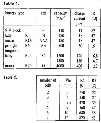
Two circuits are suggested for the incorporation in existing battery-operated equipment. Figure 1 shows the absolute minimum in the form of a simple current source. The reference voltage is obtained from the forward drop across LED D1 (about 1.5 V for a red LED). R2 fixes the current through the LED, and the voltage at the base of T1 is therefore about 1.5 V lower than the positive supply rail. The voltage across R1 is about 0.85 V, and this value may be used to determine the charge current for the battery, since A= 0.85M, independent of the circuit supply voltage.
The value of R1 is thus readily calculated if it is known that most NiCd batteries are preferably charged with a current of one tenth their capacity in amperes per hour (Ah). A number of the more popular battery types and associated values for R1 have been listed in Table 1.
A noteworthy aspect of the circuit is the fact that LED D1 will go out in the absence of a battery, since the voltage across R1 inevitably drops; the LED current which used to flow through R2 will now pass through R1 and the base-emitter junction of T1.
Table 1.
Table 2.


--------
-------
The elaborated version of the NiCd charger, shown in Fig. 2, includes a diode to protect the circuit from being damaged by input voltages having the wrong polarity. R3, R4 and T2 have been incorporated to disable the charger in the absence of a sufficiently high input voltage; Table 2 lists the relevant values for R2 and R3, given the number of 1.2 V cells contained in the NiCd battery.
Almost any type of silicon PNP transistor in the BC series should work satisfactorily in the T1 position if the charge current does not exceed about 100 mA. Higher input voltages and/or charge currents are, however, better handled by a medium-power transistor from the BD series.
The input voltage to the charger need not be elaborately regulated or smoothed; in fact, any type of inexpensive adapter providing the necessary direct output voltage and current may be used. Depending on the number of cells contained in the NiCd battery, the charge current may also be obtained from the 12 V car battery.
The circuits as shown are readily fitted on a small piece of veroboard to suit incorporation in the relevant equipment; the input voltage to the charger is conveniently connected to a small plug or socket fit ted onto the cabinet.
257 ONE-CHIP DC CONVERTER
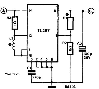
This DC step-up circuit may prove useful for the in corporation in equipment that requires the presence of a supply voltage in excess of the normal circuit supply rail of, for instance, + 5 V. Ideal therefore for generating the necessary + 8 . . .12 V voltage to feed RS232 transmitter devices, or the + 25 V programming voltage for EPROMs, the Type L497 DC converter requires very few additional passive parts to produce any of the output voltages listed in the table below.
As to the components in support of the converter chip, note L1, which is a small coil, readily made by winding about 85 turns of 34 SWG (4) 0.2 mm) enameled copper wire on a small (11 x 7 mm) pot core having an A1 rating of 160, e.g. the Siemens Type 6531-L160-A48. The total inductance of L1 should be of the order of 100 µH. Resistor R1 must be dimensioned as indicated in the table for any of the no-load output voltages. Note that the voltage across R2 is fixed at 1.2 V, and that the value of R1 may therefore be computed from R1 = (Vout - 1.2) <1 k-ohm >.
Finally, the output current may, of course, be boosted by means of a medium power transistor in a suitable configuration at the V0 output.
* Specifies no-load output voltage.
Theoretical value; select nearest E12 or E24 value.
----------
258 PRECISION RECTIFIER
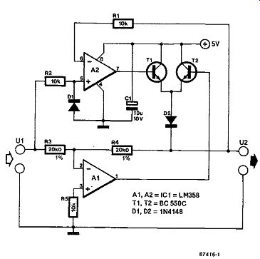
This precision rectifier operates from an asymmetrical supply, handles input signals up to 3 Vpp and has a frequency range that extends from DC to about 2 kHz. Its amplification is unity, and depends mainly on the ratio Ra/R3. Opamp A1 is connected as a voltage amplifier (Ao =1), A2 as an inverting amplifier (Ao=-1). Opamp A2, transistor T1 and diode D2 ensure that the output voltage, U2, is identical to the positive excursions of the input voltage, U1. When U1 is positive, the output of Ai is held low at about 0.25 V, so that T2 is disabled and can not affect the rectified output signal.
Components R2 and D1 protect the pnp input stage in A2 against negative voltages, which are effectively limited to-0.6 V. For negative excursions of the input signal, the function of A1, T2 and D2 is similar to the previously mentioned components.
The peak output voltage of the rectifier circuit is determined mainly by the maximum output swing of the opamps and the voltage drop across the transistors plus D2: this amounts to about 3 V in all.
When the circuit is not driven, it consumes about 1 mA, and is therefore eminently suitable for building into portable, battery-operated equipment.

------------
----------
259 SIMPLE NICD CHARGER
Dry batteries have one major disadvantage: they go flat. Rechargeable types, such as NiCd cells, also suffer from this drawback, but they can at least be recharged. Sometimes even a fifteen minute charge is sufficient to give enough life to, say, an electronic flash battery.
A NiCd charger is, in essence, nothing but a sophisticated current source. The present design contains four such sources with a common control switch, but each with a separate LED that lights as soon as a battery is connected to it.

-----------
In position 1, the sources each provide a current of about 90 mA; in positions 2 and 3 values of between 100 and 300 mA as required. Note, however, that with charging currents above about 200 mA the transistors must be fitted on suitable heat sinks.
On stability considerations, it is advisable to mount diodes D1 to D4 incl. in good thermal contact with the relevant transistors.
Terminals +B and -B enable the circuit to operate from a 12 V DC source, such as a car battery, in situations where a mains supply is not available.
Modern NiCd cells can be given a fast charge with out any problems. The present unit can charge Type AA (= HP7 = R6) cells in about 8 hours (position 1=90 mA); Type C (= HP11 = R14) cells in 10-14 hours (position 2 =180 mA); and Type D (= HP2 = R20) in 20 hours (position 3 = 200 mA).
260 SIMPLE ZERO CROSSING DETECTOR
Zero crossing detectors are often contained in rather complex circuits, or they are part of an integrated circuit, the rest of which is not required. Basically, such a detector is required to give a pulse every time the mains voltage passes through the zero potential.
The detector proposed here is very simple indeed:
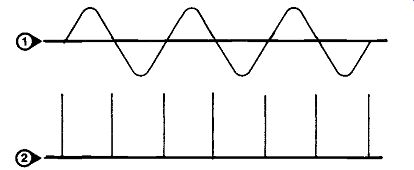
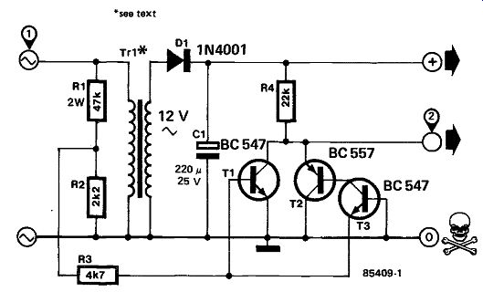
the mains voltage is transformed down, rectified in D1, and smoothed by C1 to give a direct voltage of 17 V. Part of the mains voltage is taken from across R2 and used to drive transistors T1 ... T3. During positive half cycles T1 conducts and T2 and 13 are off, whereas negative half cycles switch on T2 and T3, while T1 is off. When the momentary voltage across R2 lies between + 0.6 V and -0.6 V, none of the transistors conducts, so that the output voltage is high. In this way, a short positive pulse is produced every time the mains voltage passes through zero potential. Since operation is direct from the mains, there is no phase shift caused by the usual isolating transformer.
Where the direct voltage output of the circuit is used for supplying external circuits, attention should be paid to the current required by those circuits and the rating of the transformer. It may also be necessary to increase the value of Finally, remember that the circuit and, therefore, any external units are connected direct to the mains!
-----------
------------
261 SUPPLY PROTECTION
The use of external mains voltage adaptors for cassette recorders, portable radios, home computers, pocket calculators, and so on, is common practice since the typical enclosure sizes of this type of electronic equipment either does not allow the incorporation of a mains supply, or the device has been primarily intended for battery operation.
Unfortunately, the degree of idiosyncrasy among manufacturers of adaptors is rather high; a standard for adaptor output voltage and output polarity is definitely hard to find. It may, therefore, be quite risky to power, say, the home computer from an adaptor which is not tailored to this (expensive) piece of electronic equipment.
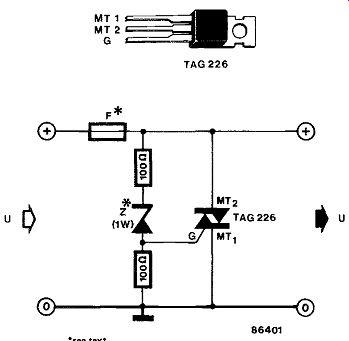
Here is a simple circuit to prevent a lot of trouble; its extremely low cost fully justifies incorporation in any equipment operated from an external DC supply. The supply protection consists of a mere four parts and a fuse, which may already be incorporated in the equipment. The zener diode is selected to have a zener voltage of about one volt higher than the equipment supply voltage.
In case the input voltage to the circuit has the wrong polarity, the zener diode conducts and causes the triac to fire, since its gate is driven positive with respect to MT2; the current flow through the triac is sufficiently high to look like a short-circuit to the fuse, which duly melts and breaks the supply voltage, before damage is inflicted upon equipment parts.
------------
Operation of the circuit in an overvoltage condition is even simpler, since in that case the zener also sup plies the gate of the triac with a firing voltage.
Obviously, if everything is in perfect order, the protection circuit is as if non-existent to the equipment it is part of, because it introduces no additional voltage drop. Finally, the only modification to the circuit for use in positive-earth equipment involves insertion of the fuse in the negative-supply line.
262 SWITCH MODE POWER SUPPLY
------------
One of the major problems in the design of switch mode power supplies is that most available (and suitable) ICs only offer the absolutely necessary facilities and not, for instance, thermal or short circuit protection.
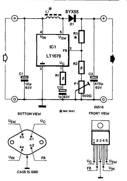
Linear Technology offers a solution to these problems with their LT1070 range of switching ICs.
These devices are as easy to use as the familiar 3-pin regulator ICs. All steps have been taken to make the design of a simple, yet efficient, switch mode supply as easy as possible. The peak output current is 5 to 9 A, and a current-limiting circuit is provided.
The diagram shows a switch mode DC-to-DC converter, whose output voltage may lie between 12 and 48 V, provided the input voltage is greater than 3 V. The input voltage of the circuit as shown must always be lower than the output voltage. It is, however, possible to modify the circuit to obtain an output voltage that is lower than the input voltage. One of the modifications is replacing L1 by a suitable transformer.
The output current is dependent on the value of the input voltage. For an input voltage of 3 V, the output power is 10 watts maximum. Our prototype, operating from 3 V, delivered about 50 mA at 48 V, while at an input voltage of 24 V the output current was over 1 A.
In the construction, account must be taken of high peak currents: all connections should, therefore, be short, and the input and output lines should be SWG20 (0.8 mm 0) or thicker. This also applies to the earth connections.
It should also be noted that spikes are present on the output voltage. If necessary, these may be eliminated by an LC filter, the inductance of which has the same value as Li, and the capacitance is between 10 and 100 µF. The quality of the capacitor is of importance because of the required low series resistance for RF signals.
263 VARIABLE 3 A POWER SUPPLY
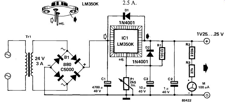
As far as construction is concerned, this is a real mini power supply, but it can deliver up to 3 A at an output voltage of 1.25 . . . 25 V. Note, however, that integrated voltage regulator IC, has on-chip overload protection that comes into operation when the dissipation in the device reaches 30 W. The ADJ(ust) pin of the regulator is connected to the junction of potential divider The output voltage, U0, is calculated from
U0 = [1.25 (1 + P1/R1)] V
where P1 and R1 are in ohms (the value of P1 is measured between the wiper and the junction with Ri, i.e., 0...2.5 k-Ohm).
Capacitor C1 is a conventional filter capacitor, while C2 and C3 improve the regulation. Protection diodes D1 and D2 ensure that at switch-off the potential at the output of IC, is more positive than that at its input. The value of R has been chosen to ensure that the minimum load current through IC, is about 3.5 A.
It is essential that IC, is mounted on a heat sink rated at about I K/W- do not scrimp on the heat conducting paste!
---------
When only low output voltages are needed, it makes sense to use a mains transformer with a lower secondary voltage (for Uo = 5 V, the secondary voltage should be 9 V). When a 24 V secondary is used, and the required output voltage is 1.25 V, the maximum output current is 1 A, otherwise the maximum dissipation of the LM 350 is exceeded, and the internal protection will switch off the regulator. When the secondary voltage is 9 V, and Uo = 1.25 V, the maximum load current amounts to 2.5 A.
264 VISIBLE POWER-ON DELAY
While in the process of repairing or testing electronic equipment, it is often desired to have more time available for hooking up an oscilloscope probe or test lead to the part in question, after power has been applied.
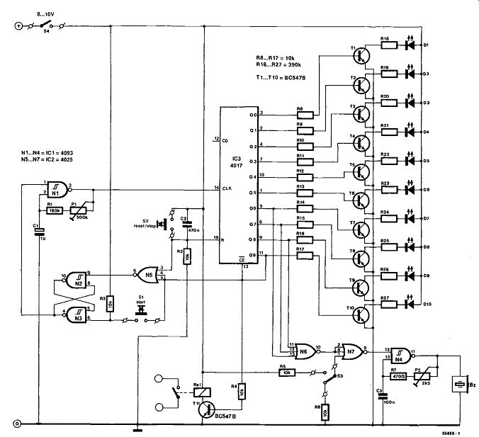
This circuit gives you plenty of time to reach any component in the circuit, since the equipment is only switched on after a fixed interval following depression of the start button.
The basic operation of the circuit is as follows. Activating start switch S1 sets the bistable composed of N2 and N3, causing N3 to provide clock pulses to decade counter IC3. The driver transistors at the outputs of this IC will light the LEDs one after another, indicating the countdown function of the circuit. Re1 is energized the moment the last LED in the row lights; IC3 is disabled via its CE input, and the N2-N3 bistable is reset, all at the same time. The equipment, powered over the relay contacts, is turned on, and the user may take the desired reading.
The power-on interval may be restarted or interrupted during countdown by depressing S2, which resets the bistable and counter.
During the final three stages of the countdown, a warning buzzer is arranged to sound by means of N4; this function may be disabled by means of S3.
Re1 should not consume more than 100 mA of coil current, while its contact(s) should be rated to suit the load to be switched.

--------------
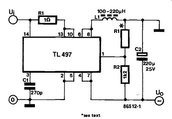
265 VOLTAGE INVERTER
Here is a circuit that produces a negative voltage from a positive one, for instance, from +5 V to -10 V. The output voltage, U0, is determined from U0 =-1.2(Ri/R2 + I)
As in other, similar circuits, the maximum output current depends on the ratio between input and output voltage and is calculated from iolmax) = 500/(R1/R2 + 1) [mA] The choke is readily made with a 17.5 mm pot core on which 85 turns of 0.2 mm^2 enameled copper wire are close-wound.
The maximum input voltage to the IC is 15 V. Efficiency is of the order of 60 percent.
-------