266 8-CHANNEL VOLTAGE DISPLAY
Simultaneously monitoring the trends of 8 slowly varying voltages is normally very difficult, if not impossible, even with the aid of 8 analog or digital voltmeters. This circuit turns a common oscilloscope into a versatile 8-channel display for direct voltages. The trend of each of the 8 input levels is readily observed, albeit that the attainable resolution is not very high.
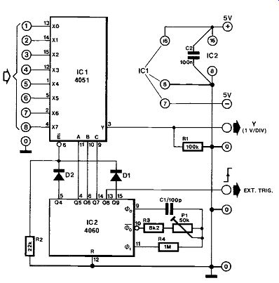
The circuit diagram shows the use of an 8-channel analog multiplexer, IC1, which is the electronic version of an 8-way rotary switch with contacts X0-X7 and pole Y. The relevant channel is selected by applying an binary code to the A-B-C inputs.
Example: binary code 011 (A-B-C) enables channel 7 (X6-.Y). The A-B-C inputs of IC1 are driven from three successive outputs of binary counter IC2, which is set to oscillate at about 50 kHz with the aid of Pt As the counter is not reset, the binary state of outputs Q5, Q6 and Q7 steps from 0 to 7 in a cyclic manner. Each of the direct voltages at input terminals 1 to 8 is therefore briefly connected to the Y input of the oscilloscope. All eight input levels can be seen simultaneously by setting the timebase of the scope in accordance with the time it takes the counter to output states 0 through 7 on the Q6-Q6-Q7 outputs. The correct starting time for the oscilloscope trace is ensured by using the Q8 output of the counter to supply the trigger pulse. Diodes D1 and D2 provide for some space between adjacent bars on the display, and create a horizontal reference line.
The timebase on the scope should be set to 0.5 ms/div, and triggering should occur on the positive edge of the external signal. Set the vertical sensitivity to 1 V/div. The input range of this circuit is from -4 V to +4 V, and connected channels are terminated in about 100K.
Adjusting the 8-channel voltage display is straight forward. Simply select the previously mentioned scope settings, and adjust P1 to make all 8 channels visible over the full width of the scope screen-see the accompanying photograph.
---------
The circuit has a modest current demand of less than 5 mA from a simple ± 5 V supply, or from two 4.5 V flatpack batteries.
267 AUDIO TESTER
A simple millivoltmeter and an equally simple sine wave generator are ideal instruments for checking and testing audio equipment. The audio tester combines the two, as shown in figure 1, where A1 and A2 form the millivoltmeter circuit, while the sine wave generator is built from A3 and A4.

--------
Parts list
Resistors:
= 1 M R2 = 6k8 133 = 68 k R4,R5 = 150 k R6,R9 = 1 k R7 = 100 R. = 15 k R10,R11 = 2k2 R12 = 4k7 R1a,R14 = 100 k R15 = 8k2 R16 = 82 k R17 = 470 ohm Pi = 25 k preset (see text) P2 = 1 M stereo preset, log.
P3 = 5 k preset
Capacitors:
= 1 p metallized plastic foil
C2,C6 = 100 p/10 V
C3,C4 = 4n7 C7 = 560 n
C. = 220 p/16 V Semiconductors:
D1 ...D6,D8,D9 = 1N4148
D7 = zener diode 4V7/0,4 W
T1,T2 = BC 547B IC/ = TL084
Miscellaneous:
M1 = moving coil meter, 50 pA (see text)
PP3 (9 V) battery with dual miniature clip
SPST on/off switch (optional- see text)
PCB 84923
As the audio tester is supplied (asymmetrically) from a 9 V battery, this supply must be halved for the operational amplifiers. This is essentially done by zener diode D7. This zener is biased by R6, and the reference voltage is taken from the junction of diodes D8-D9 via resistor R7. The reference voltage is, therefore, about 5.3 V. The constant voltage drop across the two diodes is applied across preset P3 which serves to negate the offset voltage of A2 (enabling the millivoltmeter to be calibrated to zero).
The input signal is applied across high pass filter C1/ R1 to the non-inverting input of A1. For all practical purposes, this sets the input impedance at 1 M4. Note that the circuit is fully driven with an input signal of 50 mVrms. Higher inputs necessitate a voltage divider at the input or a reduction in gain in A1 by dropping the value of R3. When this resistor is reduced to 6k8, for instance, the gain of A1 is 2, and the input sensitivity is 275 mVrms.
Full-scale deflection of the meter is set by P1. Opamp A, together with diodes D3 . . . D6, functions as an active full-wave rectifier. The meter is connected in of the diagonals of the diode bridge. To ensure that even small AC voltages can be measured, the potentials at both inputs of A2 must be absolutely equal. Because of this, a small offset voltage is applied to the non-inverting input via Rs.
The sine wave generator is essentially a Wien bridge oscillator, A2, whose frequency determining components are P4 C3, and C4. To ensure stable operation, an active feedback loop takes part of the output signal of buffer amplifier A4, rectifies this (Dl, D2) and applies the consequent DC voltage to the inverting input of A3 via buffer stages T1 and T2 The output voltage of the generator section is 2 Vpp.
The audio tester is best constructed on the printed circuit board of figure 2. The meter can be almost any type from 50 µA to 1 mA. Note, however, that the value of 131 in figure 1 applies to a 50 µA instrument; for a different f.s.d., this value can be changed inversely proportional. For instance, if the instrument is a 500 µA type, P1 should be 2k5.
The millivoltmeter is calibrated by tapping the reference voltage with a divider of 820 ohm in series with 100 kQ: the voltage at their junction will be 45 mV.
Apply that voltage to the non-inverting ( +) input of A1, and adjust D1 till the meter reads "45".
The current consumption of the audio tester is some 10 mA, and it is therefore advisable to incorporate an on/off switch. The frequency range extends from 150 Hz to 20 kHz.

-------------
268 AUTOMATIC SWITCH OFF
If you are one of the many who frequently forget to switch off their digital multimeter, this circuit is for you.
-------------
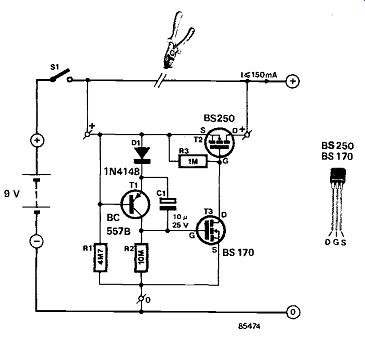
When this little circuit, which is intended to be incorporated in the multimeter, is switched on, capacitor C1 is connected to the +9 V line via D1.
Since C1 is discharged, the gate of T3 is also at +9 V which causes T3 and T2 to conduct. The meter is then switched on.
Capacitor C1 slowly charges via R2. After about 2 or 3 minutes, the potential at the gate of T3 becomes too low to keep the FET in conduction.
Transistor T2 then also switches off, and the battery is disconnected from the multimeter.
Transistor T1 ensures that when the multimeter is switched off manually, capacitor C1 is discharged.
When the multimeter on/off switch, S1, is opened, a base current will flow to the negative terminal of C1 via R, and R2. Transistor T1 then conducts and discharges C1. The circuit is thus immediately ready for use again. Without T1, there would have to be a delay of a few minutes before the circuit could be switched on again.
The circuit is best built on a small piece of veroboard and then fitted between the on/off switch and the meter itself.
A final tip: T2 could be replaced by a Darlington, such as a BC516, in which case a 1-M-ohm resistor would have to be inserted in the connection to the drain of T3. This .arrangement would have the ad vantage that the BC516 is more easily obtainable than the BS250, but the disadvantage of causing a slightly larger voltage drop across the circuit: 0.8 V as compared with less than 0.1 V when a BS250 is used. The current in both cases is 10 mA.
269 CALIBRATION GENERATOR
A calibration generator is of particular use with many older generation receivers, which have no, or a poor, frequency read-out. However, the RF section of these receivers is invariably far superior to that of most modern models, and consequently there are still many of these `oldies' in use.
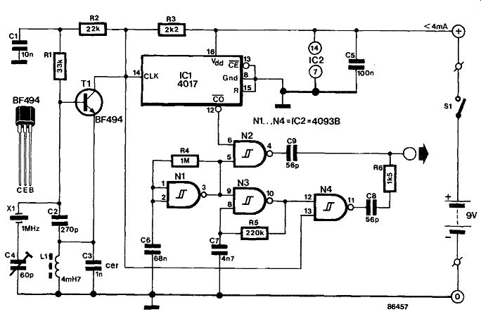
The circuit in the accompanying diagram provides calibration signals at multiples of 100 kHz and 1 MHz, all of which are available simultaneously, so that no switching is necessary.
The output signal of the crystal oscillator, T1, is divided by 10 in IC1 . Astable Ni operates at a frequency of around 22 Hz, which is low enough to allow zero beat tuning even in SSB operation. The 100 kHz harmonics sound (on AM) like a sort of woodpecker.
Astable N3 operates at about 1.5 kHz and is gated with the 22 Hz signal. Consequently, the 1 MHz signal appears for 22 ms as a carrier wave, which is modulated with the 1.5 kHz signal during the next 22 ms. This signal is also easily tuned for zero beat.
The circuit is usable up to 30 MHz when CMOS devices are used, and up to around 300 MHz with HCMOS ICs.
--------
270 CRYSTAL TESTER
Many electronics hobbyists have crystals lying about, but don't know whether these .are still working all right. The crystal tester described here will quickly show whether a crystal can be used or should be discarded.
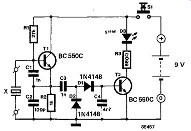
Transistor T1 and the crystal under test form an oscillator. Capacitors C1 and C2 form a voltage divider in the oscillator circuit. If the crystal is in good order, the oscillator will work. Its output voltage is then rectified and smoothed by D1 and C4 respectively. The resulting direct voltage at the base of T2 is sufficient to switch this transistor on, so that the LED lights.
The circuit is suitable for use with crystals of a frequency between 100 kHz and 30 MHz. Current consumption is about 50 mA.
--------
271 DIVIDER CASCADE
This circuit can be driven either with an analog, or a digital precision 10 MHz signal for dividing down to a number of commonly used timebase periods. The oscillator proposed in (1) is particularly suitable for driving the present cascade, since it offers excellent stability thanks to the use of I 10 MHz quartz crystal fitted in an electronically controlled oven. It should be noted, however, that its output is digitally compatible, so that components R1-C1 and R2 at the input of the circuit shown here can be omitted, i.e., N1 is driven direct.
Where an analog, sinusoidal, 10 MHz signal is used, the amplitude must be 750 mVpp. Evidently, R(-C) and R2 are then required to make the signal digitally compatible for clocking IC3. The circuit diagram shows that the cascade can be extended by adding further 74HC(T)390s and pairs of bistables.
The Type 74HC(T)390 (IC3) holds two counters, the first of which divides by two (1QA), and by 5 (IQc). Bistable FF is driven with the IQD output, and outputs the :10 signal, which is also applied to the CLK inputs of the second counter in IC3. This also divides by 2 and 5, while FF2 gives a total division factor of 100 in the first block of the cascade. The use of decade counters results in output periods commonly used for an oscilloscope timebase. Counters and bistables may be added to obtain relatively long, yet accurately defined, periods for specific applications. The current consumption of the circuit as shown is about 12 mA.
With two divider blocks added, the total current drain is expected to be approximately 25 mA, not 36 mA, since HCMOS circuits require less power at lower clock frequencies.
Reference:
(1) Oven-compensated oscillator. Elektor Electronics, January 1986.

------
272 FAST VOLTAGE-CONTROLLED PULSE GENERATOR
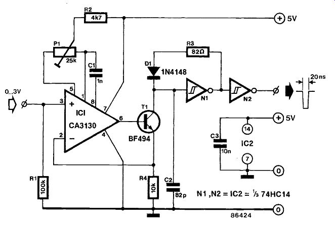
Certain measuring and process control applications require pulse generator sections which are to operate over a large frequency range and must, therefore, produce a signal with very low pulse width. It is for this reason that the proposed circuit uses high-speed complementary MOS (HCMOS) type gates; the prototype typically produced an output pulse width of 20 ns over the frequency range of several hundred hertz to 25 MHz.
The combination IC1- T1 is a voltage-controlled current source which discharges C2. The fast charging of this capacitor is effected through the voltage at the output of Schmitt trigger N1-R3-D1. The lower frequency limit of the proposed circuit mainly depends on the offset voltage of opamp IC1. In order to enable setting the lower frequency limit, Ts must be arranged so as not to draw any current at an input voltage of 0V; to this end, offset preset P1 should be correctly adjusted. Finally, the output pulse width may be widened by increasing the capacitance of C2; this will not alter the attainable sweep range.
Literature: E Abbel, Electronic Design 18 (1984), pp 270-271.
------------
273 FAULT-FINDING PROBE FOR µPs
Anyone who has ever tried to fault-find in a microprocessor system with a test probe will have experienced the uselessness of it. This is because the signals at the address, data, and control buses are constantly- and rapidly- changing. This means that it is not just the signal level that is important, but also the instant the signals are present. For faultfinding properly, you need a logic analyzer, which is capable of indicating several signals simultaneously.
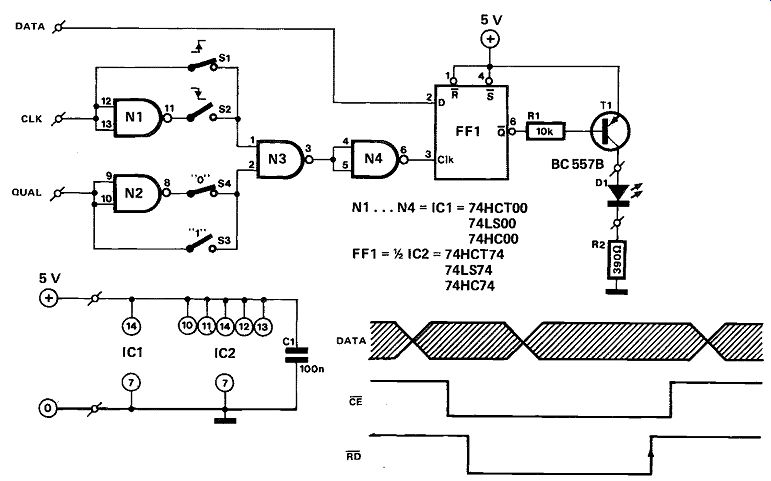
If you have no logic analyzer, the probe presented here may provide the solution. Strictly speaking, this is nothing more than a bistable multivibrator (FF1). Data are simply read direct and cause D1 to light or stay out, depending on the state of FF1.
The bistable only reads at the instant its clock input (pin 3) switches from low to high).
The clock signal is thus the key for all measurements carried out with the probe and that means it must be chosen with some care for every test. Suppose you have to check whether a certain portion of memory is all right. The CE signal in the memory is then connected to the QUAL input of the probe. Switch S4 must be closed, because CE is active low. The probe can then only read data during a CE of the RAM under test. The CLK input of the probe is connected to the RD signal of the memory. Reading must then be carried out during the trailing, i.e., the positive-going, edge. Switch S1 must, therefore, be closed. Reading is effected by, for instance, a PEEK command in BASIC. Diode D1 will then light in accordance with the signal emanating from the RAM during this process.
Be careful that this BASIC is not used by the RAM section being tested, because then there will be more than one read process and the probe will only retain the last of these. There is no easy solution in that case, but often it will be possible with the aid of a monitor to make the microcomputer execute only one command in machine language.
To keep the probe small, DIL (dual in line) switches are used in the S1 . .S4 positions. Note that only S1 or S2 and S3 or S4 should be closed simultaneously at any one time.
LS type ICs may be used, but as these put a relatively high load on the circuit during tests, HCT types are better. These are fully compatible with the IS types but have high impedance inputs. HC types should only be used where systems are already executed entirely in CMOS; the supply voltage can then be higher than 5 V.
Current consumption of the circuit is small: 10 mA for the LED and and 5 mA for the ICs (if these are TTL).
-------
274 FUNCTION GENERATOR
This is a downright simple design for an AF function generator that supplies a rectangular and triangular signal, and can be fed from a single 9 V supply. The signal generator proper is a Type TLC272 dual CMOS opamp from Texas Instruments. This chip is remarkable for its low current consumption and wide operating range.
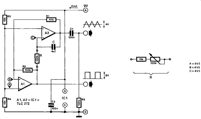
The circuit is essentially composed of two functional parts. Opamp A1 is connected to function as a Schmitt-trigger whose toggle point is set to 4.5 V, while A2 is an integrator that converts the rectangular signal from At into a triangular waveform.
The oscillation frequency of the circuit is fixed solely by the ratio RC and can be calculated from fo = R2/4RR,C. Resistor R may be replaced by the combination of the 10K resistor and 100K potentiometer as shown to effect continuous adjustment of the output frequency within the AF signal band.
The generator should not be terminated in less than 10K.
-----------
275 GHZ PRESCALER
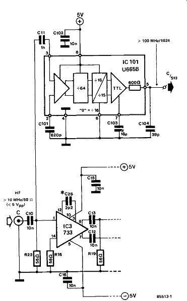
In the 1.2 GHz input stage (February 1985) for the microprocessor-controlled frequency counter, we used an SB8755 prescaler in the IC7 position. This IC, which divides the 100 .. . A200 MHz signal at input C by 512, is perfect for the purpose, but is rather expensive. Just recently, another prescaler, which is much cheaper and more sensitive, has come onto the market: the U665B from Telefunken.
The U665B is a 1024 prescaler with integral pre amplifier. Its sensitivity is better than 10 mVrms for frequencies between 80 MHz and 900 MHz. It is fully usable up to 1200 MHz, but its sensitivity drops to about 30...40 mVrms at that frequency.
To fit the U665B onto the PCB, first remove existing IC7, IC8, and P3. No other components should be removed because, although they may look superfluous, they are needed for the interconnection between the component and track sides of the board.

---------
--------
The new IC is fitted so that its pin 1 coincides with pin 8 of the previous IC7. Next, solder capacitors C1 0 1, C1 0 2, C103, and C104 direct to the relevant pins of the new IC and to the earth plane. Then, solder pins 4 and 6 direct to the earth plane and place a wire link between pin 8 of the U665B and the hole where pin 1 of IC7 used to be (see drawing). Finally, solder a wire link between the holes where pins 1 and 11 of IC8 used to be.
So much for the hardware; now something about the software. The U665B divides the input frequency by 1024, while IC7 + IC8 divided by only 512. This difference means that one byte in the EPROM must be altered: address $627 reads $09; this should be amended to $0A.
276 INSTRUMENTATION AMPLIFIER
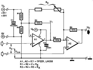
This instrumentation amplifier was originally de signed for the serial digitizer described in (1), but should be suitable for many other applications also.
The amplifier makes it possible to use a relatively long, interference-free, connection between the transducer or sensor and the digitizer input.
The theoretical basis for the circuit is summarized in the accompanying Table. It is seen that the common mode rejection of the amplifier serves to sup press interference. In practice, however, the low drive margins of the inputs and outputs of the opamps impose some limitations. Both suggested types have PNP input transistors capable of hand ling input voltages between 0 and Ub-1.5 V. The output of the OP-220 can deliver voltages between 0 and Ub-1 V, that of the LM358 between 0 and Ub-1.5 V.
The current consumption of the opamps is low at about 150 µA for the OP-220, and I mA for the LM358, while the slew rate is about 0.04 V/µs and 0.4 V/ms respectively. For optimum accuracy it is recommended to use high stability (I%) resistors in positions R1-R5 inclusive.
----------
PMI Application
Reference:
(1) Universal peripheral equipment (2): Serial Digitizer. Elektor Electronics, September 1986 p. 23 ff.
-------- Micropower instrumentation amplifier
Consider an input UCM-1/2Ud at the- input of the circuit, and UCM+ 1/2 Ud at the + input. This corresponds to a common-mode input UCM, and a differential input Ud. The currents at the inverting input of each opamp can be summed to form two equations:
(Ub-UCM+ 1/2Ud) (1/R1)+(Ud/Ro)+(U1+ 1/2 Ud) (1/R3) = (UCM - 1/2 Ud) (1/R2) (1)
(Ui =UCm-1/2Ud) (1/R4)+Uo-Y2Ud) (1/R5) = Ud/Ro
When Re =R2= 2R3=2R4 = 2R5= 2Rx, (1) and (2) can be combined to:
Uo= 2(1 +Rx/Ro)Ud + 1/2 2 Ub
... which shows that the common mode input (UCM) has been rejected. The differential gain, Ax, of the circuit is therefore:
Ax = 2+ (2Rx/Ro)
.... and is adjustable between 0 and 1,000 by varying Ro.
(2)
----------
277 LINE BAR GENERATOR
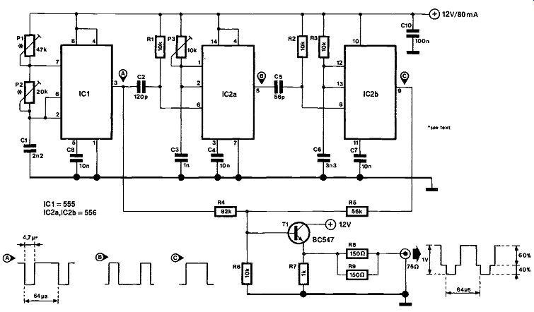
The video signal transmitted by most TV broadcast stations is rather complex. For most tests and experiments, however, a fairly simple signal will suffice. The circuit presented here provides a small, in expensive source of line synchronizing pulses and line bar.
The first of the three timers in the diagram provides 4.7 pis sync pulses. It is arranged as an astable multi-vibrator with a period of 64 his. The rising (here: negative-going) edge of the sync pulse triggers a second timer. The width of the output pulse of this timer determines the position of the line bar. The line bar proper is provided by the third timer. To obtain a usable video signal, the sync and bar signals must be added, which takes place in R4-R5-R6. The resistor network is followed by a buffer that ensures an output impedance of 75 ohms. The unit can, therefore, be connected direct to a standard video in put. The sync and bar signals occupy 40 percent and 60 percent of the composite signal respectively.
Calibration is carried out by connecting the unit to a monitor or, via a modulator, to a normal TV receiver. Presets P1, P2, and P3 are set to the center of their travel. Turn P1 to obtain a still picture. If the sync pulse is too wide, it will be visible at the left hand side of the picture. The pulse may be narrowed with the aid of P2, after which P, may need a small re-adjustment.
------------
Where an oscilloscope is available, P2 can initially be set to obtain 4.7 us pulses at the output (pin 3) of IC,. Then, the total period is set to 64 us with the aid of P1. The line bar is centered with P3: as its width is fixed, this completes the calibration.
278 LOGARITHMIC SWEEP GENERATOR
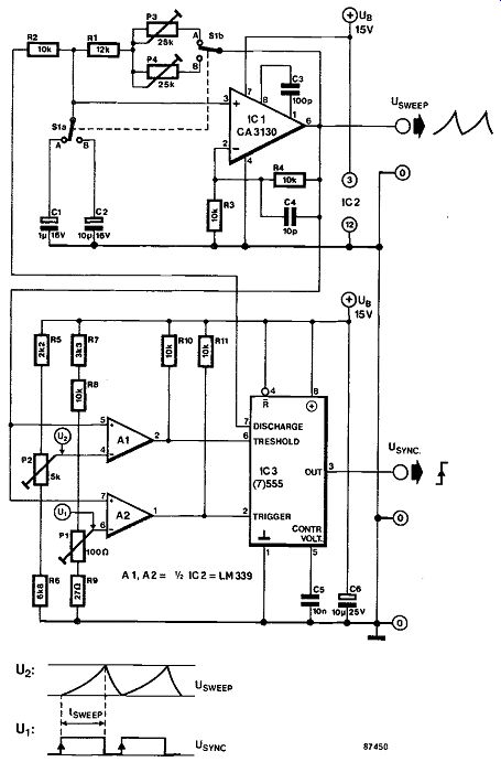
This circuit outputs a logarithmic signal for driving the VCO input on the Elektor Electronics Function Generator (1), but can be used for other generators as well. Usually, the exponential function is derived from the (temperature-sensitive) B-E junction in a transistor, but this design uses a simple R-C net work and an opamp to generate the logarithmic sweep.
With reference to the circuit diagram, Us is applied to the generator's VCO input, while Usync is used for triggering an oscilloscope on the positive signal edge. Contrary to the Elektor Electronics Sweep Generator in (2), the timebase of the scope is used for the horizontal deflection, so that the horizontal (frequency) axis has a logarithmic scale. The sweep range is 1:100 (Uvco =0.1-10 V). Opamp IC2 is dimensioned for a gain of 2 (R3-R4) and generates an sweep voltage, Us, with the aid of network P3/134-R1-C1/C2:
Us = U1exp(t/R1C1) when
U1<Us<U2.
When Us reaches level U2, the bistable in IC3 is reset.
Capacitor C1 (or C2) is then discharged via R2 and the discharge input on the 555 (or 7555) until Us = U1, causing IC3 to be set and the next sweep period to commence. The output of the monostable supplies the trigger signal for the oscilloscope.
To adjust the circuit, set the function generator to 100 Hz; external frequency. Connect the VCO in put to the wiper of P1 (do not forget the ground connection), and adjust this preset for an output frequency of 100 Hz. Next, connect the VCO input to the wiper of P2, and adjust this preset for an output frequency of 10 kHz. Proceed with connecting the oscilloscope, set to 10 ms/div., external trigger. The sweep voltage is applied to the Y input, and the vertical sensitivity is adjusted until the maximum excursion of Us reaches the top of the display. Set S, to position A (sweep 0.1 s), and adjust P3 until the peak of the exponential voltage is displayed in the top right-hand corner. This is repeated with S1 set to position B (sweep 1 s), and the scope set to 100 mV/div. (adjust P4). This completes the adjustment procedure, and Us can be connected to the VCO input. The current consumption of the circuit is less than 25 mA or 15 mA with a 555 or a 7555 fitted, respectively.
References:
Function generator. Elektor Electronics, December 1984.
(2) Audio sweep generator. Elektor Electronics, November 1985.
--------
279 LOW CURRENT AMMETER
This 7-range ammeter measures currents between a few pA to 100 µA without using precision resistors with very high values. The circuit is set up around a current mirror Tra-Tib. The input current is mirrored in this transistor pair, and the current through T1b is greater than the input current by a factor set with Si. Meter M1 is a 100 µA fsd type for displaying the measured value. The effective series voltage drop at the input terminals of the instrument is only 500 µV because the voltage across the inputs of A) is forced to virtually zero.
The accuracy of the ammeter depends mainly on the components used. Depending on the required precision, certain components may be replaced by types with a better specification. The Type LF411 opamp used in the Ai position, for example, can be replaced with the Type OP-41 to achieve a tenfold reduction in the input bias current, and hence an improvement in the final accuracy of the instrument. Transistor pair T1a-Tib may be replaced by a Type MAT-02, and the voltage reference set up with T3-T4 by a Type LM313. These high-quality parts should ensure an accuracy of 1% over most of the range. The meter is calibrated in the 1µA range.
Preset P1 is adjusted for full scale deflection of MI at an input current of 1µA.
When it is intended to make a printed circuit board for the pico ammeter, it should be borne in mind that two 2.5 cm long, parallel running, copper tracks spaced 1.25 mm and etched on a high quality epoxy/ glass carrier represent a leakage resistance of about 100 G-Ohm. This corresponds to a leakage current of 150 pA at a voltage difference of 15 V. Evidently, the PCB for the present ammeter should be thoroughly cleaned to rule out leakage current through residual moisture or resin. Also note that the insulation of standard test leads is likely to make reliable measuring of currents smaller than 1 pA impossible. The only way to overcome this difficulty is to use dry air or FTFE (Teflon).
Source: PMI Linear and Conversion Applications Handbook.

------
280 MEASURING WITH THE BBC MICRO
The BBC micro, one of the best value-for-money computers on the market, can be used for a variety of applications thanks to the various interfaces provided as standard. The four analog inputs, each with a resolution of 10 bits, make it particularly suitable for measuring all kinds of processes.
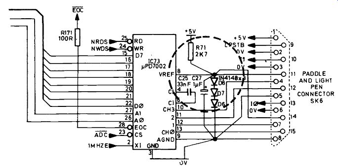
There is unfortunately one drawback: the rather poor reference voltage associated with the analog inputs. That voltage is obtained from three normal diodes connected in series. The alternative de scribed here has been in use in our BBC micro for some time.
Diodes D6 . . . D8 in the diagram provide a reference voltage of 1.8 V, which is fine for use with a joystick interface, but will not do where absolute values are to be measured. The three diodes are, therefore, re placed by one zener diode, a 2.5 V type LM336Z.
This diode deviates no more than 1.8 mV over the temperature range of 0 . . .70 °C; its long-term stability is better than 20 p.p.m. at 25 °C. Its internal resistance is 0.4 2, which makes it ideal for our purpose. Moreover, it is easily fitted into the micro without the need for any alterations other than the removal of D6 . . . D8. The micro remains, of course, fully compatible with existing software.
Cut off the adjust terminal from the LM336Z, and unsolder D6 . . D8 from the computer. Solder the anode and cathode of the zener to the cathode connection of D6 and the anode connection of D8 respectively. A good-quality small soldering iron is in dispensable here!
-----
281 METER AMPLIFIER
A meter amplifier is intended for use between a sensor or other measuring device, such as a probe, and the indicator. It is characterized by a high input impedance, typically 1 MQ, and a differential input.
A differential input ensures that the output signal cannot be affected by hum or noise on the meter leads.
The input signals are buffered by differential amplifiers A1 and A2. The 22 pF capacitors in the C1 and C2 positions obviate any tendency to oscillate. The output of opamp A3 is a function of the difference between the two input signals.
Opamp A4 serves to compensate for any offset and also to set the amplification at exactly 1. The band width of the circuit as shown is not less than 100 kHz, and the phase shift is 0°.
As already mentioned, the amplifier may be used with any sensor, for instance, in computer control of the central heating, or to monitor the ambient temperature in rooms. It can also be used with a multimeter or oscilloscope.
The peak-to-peak level of the input signal should not exceed about 80 percent of the supply voltage.
Current consumption is not greater than 25 mA at a supply voltage of ± 18 V.
Calibrate the unit by adjusting P2 under no-signal conditions for zero output, and setting the amplification to exactly 1 with Pt If you aim at perfection, use 1 percent resistors.

--
282 METERING SELECTOR
When just one meter is used to measure the voltage of three different sources, it is, of course, possible to use a three position rotary switch to select any one of the sources. However, care must be taken here, because the switch must break before make, otherwise two sources are interconnected and this is normally highly undesirable.
Any electronic equivalent of the rotary switch must, of course, also break before make. Unfortunately, transistors have the property of switching on much faster than switching off. For example, a well-driven BC 547 takes a couple of 1.4s to switch off, but far less than that to switch on.
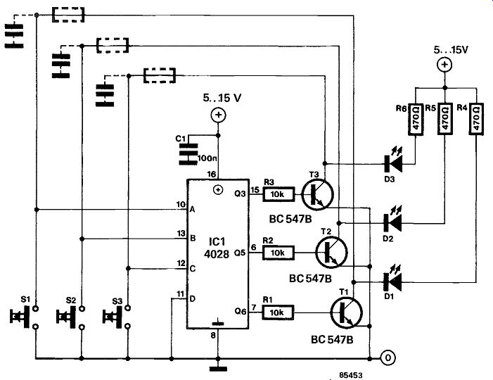
The present circuit circumnavigates these potential troubles by using the output level as criterion, whereby a 4028 serves as the referee. The 4028 is a one-of-ten active high decoder which drives one of three transistors, T, . . . Ta Let us assume that T1 is on: its collector voltage is low, and so is input A of the 4028. The other two collectors are high, and so are inputs B and C of the decoder. The 4028 therefore sees binary code 6 (110) at its input and this causes pin 6 to go logic high, so that T1 is driven hard.
When in this condition another key, for instance, Sz2, is pressed, a wrong code, i.e., 4 (100), ensues. output 4 of the 4028 is, however, not connected, T1 switches off, but T2 is not yet driven. Only after T1 has actually switched off, and its collector goes high, does 5 (101) arise at the input of the 4028: T2 will then be driven.
In practice, the voltage at the collector may be used to control a CMOS switch that arranges the change over of the meter or the sound channel. It is also possible to replace the collector resistor by a suitable relay, but this would, of course, introduce even longer delay times (of the order of milliseconds). In that case, the feedback to the input must be effected by a separate contact of the relay, but there is then, of course, absolute certainty that switching is correct! Another variant is including a resistance in each feedback loop and shunting each switch contact by a capacitor. This RC network will ensure a reasonable delay during the change over.
Current consumption of the 4028 is small (CMOS!), while that of the transistors depends on the value of the collector resistors. With values as shown, it amounts to 18 mA for a supply voltage of 10 V.
-----------
283 NOISE GENERATOR

--------
Noise is normally defined as unwanted electrical signals spread over a relatively flat, wide frequency spectrum. In most equipment, great care is taken to reduce the amount of noise to a minimum, resulting in a low noise factor.
Nonetheless, noise is useful for measuring the behavior of a circuit under varying input conditions. A noise generator is used, for instance, for measurements on coaxial cables, microwave links, and RTTY (radio teletype) and CW (continuous wave = radio telegraphy) decoders. The present circuit may also be used to imitate the sound of wind, mosquitoes, bees, and other buzzing insects.
The circuit consists of a relaxation oscillator, IC,, which is provided with positive and negative feed back via D1-R2 and P3-P2-R3-C1 respectively. Zener diode D1 functions as noise source. The amplification of the noise is determined by the setting of
P3 (coarse) and P2 (fine). The setting of P1 deter mines the noise bandwidth: a small effective value results in a narrow band, and increasing values cause wider bands.
Due to the negative feedback, the opamp also functions as a low-pass filter: a small feedback factor results in a low roll-off frequency. The pass band of the opamp also depends on the value of C2: a value of 47 n causes a noise similar to the buzzing of a mosquito or bee. Diodes D2 and D3 serve as input limiters. The output level of the generator can be adjusted with P4 Current consumption is not greater than 10 mA at 12 V.
284 OPAMP TESTER

------
All types of operational amplifier can be functionally checked with the tester proposed here.
The principle of the tester is quite simple: a triangular voltage is applied to the inverting (-) in put of the specimen. This voltage is, of course, inverted. If then the inverted and the original triangular voltage are added, the result should be zero. Any deviations from this are taken as a mal function which is indicated by one of two light-emitting diodes (LEDs). The tester has, of course, a self test facility so that the error-free operation of it can be readily ascertained.
Opamps A1 and A2 form a triangular pulse generator. Opamp Ai operates as an integrator: capacitor C1 is charged, and as soon as the voltage across it reaches the threshold value of Schmitt trigger A2, resistor R4 is connected to earth, and C1 discharges until the voltage across it reaches the second threshold of A2, when the process repeats itself.
Opamp A3 functions as the summing stage whose output is fed to two transistors that drive LEDs.
The specimens are connected as inverters in either positions Ap1 Ap4 or Ap5. In the design it was assumed that the most frequently encountered opamps are contained in a 14-pin DIL housing (as, for instance, the TL 084 used for A1 . . A3), or in an 8-pin DIL package (such as the LM 355 or LM 387). For different packages, the specimen connections in figure 1 should be modified accordingly.
When a specimen is defect, the output of A3 consists of a triangular voltage superimposed on the (DC) offset. This is sufficient to bias the drive transistors and one or both LEDs flash in rhythm with the triangular voltage. The frequency of that signal is about 10 Hz, and this can be altered to some extent by changing the value of R4 and/or It is clear that the voltage at the output of A3 must be greater than ± 0.6 V, otherwise the bias for the transistors is too small. Preset Pi should therefore be adjusted so that the LEDs just do not light when an opamp that is known to work correctly is inserted in the relevant specimen position.
The self test function is easily checked: when P2 is turned from one extreme of its travel to the other, first one LED, then both, and finally the other LED should light.
In positions 1 . . . 4 of switch S1, the four opamps contained in, say, a TL 084 can be tested sequentially; in position 5, the single opamp contained in, say, an LM 355; and position 6 is the self test set ting.
285 POCKET FREQUENCY METER
This easy to construct circuit meets the demand for a simple, yet versatile battery operated frequency meter which can interpret signals with a minimum rms voltage of 10 mV and a maximum frequency of 100 kHz. The quiescent current consumption of the meter circuit is only 4 mA, which ensures a long life for the 9 V battery. Also of interest is the fact that the circuit continues to work normally with battery voltages down to about 5 V. The meter input is protected up to 250 V AC.
From the circuit diagram it is seen that the input signal is applied to the gate of T1 via R1 and C2. C1 is an additional speed-up capacitor to improve the response at higher frequencies, while anti-parallel connected diodes D1 and D2 protect the FET gate from high voltage surges. T1 functions as a buffer, preceding Schmitt trigger Ai, which has been dimensioned for a relatively low hysteresis of about 18 mV to prevent the overall sensitivity being too strongly degraded. The output of A1 is fed direct to divide-by-two counter IC1a, which is followed by three cascaded divide-by-ten IC sections. S2 selects the divisor and hence the relevant frequency range.
Whatever range is selected, a frequency of 50 Hz at the pole of S2 corresponds to a full scale reading on moving coil meter M.
The signal at the pole of S2 is used to trigger the monostable built around the Type 7555 low-power precision timer. The correct operation of this circuit section can only be achieved if the time period of the monostable is less than half that of the full scale frequency, i.e. 1/2(1/50)s = 10 ms. Therefore, a monostable time of 8 ms is used in the proposed configuration.
The output signal from IC3 has a duty factor which is proportional to the input signal frequency.
The pulses from IC3 are leveled at 2.5 Vpp by IC4, before being integrated by Riz and Cs to produce a direct voltage which is proportional to the input frequency. The circuit around A2 and T2 is a simple voltage-to-current converter with the 100 µA moving coil meter connected in the collector supply line to T2. C9 may be added to stabilize the read-out at the lower end of the scale.
Though a Type LM393 opamp has been used, the less expensive Type LM339 also works all right, provided the inputs of the unused opamps contained in this chip are tied to the positive supply rail to minimize their power consumption.
The frequency meter is so sensitive that merely touching the input terminal with a finger causes the meter to read the mains frequency. This is, incidentally, a convenient method of calibration, since Pi may be set to give a reading in accordance with the local mains frequency, which is usually stable within 1%.
286 PROGRAMMABLE BAUD-RATE GENERATOR
Only some computers, e.g., the Samson 65, enable you to reprogram the ACIA (asynchronous communications interface adapter), or whatever your serial interface may be, if you want to connect a printer and a modem to your computer. With most other micros, you have to use an additional circuit like the one proposed here.
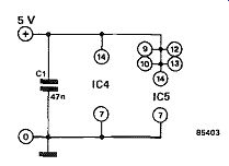
The circuit is based on a pre-settable, synchronous down counter, a CMOS IC type 40103. Another CMOS IC, type 4060B, serves as a crystal con trolled clock generator. The crystal frequency, fx, is 2.4576 MHz, while the clock, fc, is 153.6 kHz. The output frequency, fo. of the generator is determined from fo = [153.6/(N + 1)] kHz where N is the decimal equivalent of the number that is input to the JO . . J7 terminals of the 40103 (see table).
The number N is provided by the computer and from there written into, and stored by, the 74LS374.
The table gives various baud rates (also for RTTY-radio teletype) and the corresponding decimal and hexadecimal numbers. If you want to shift the baud range upwards, select a higher value output of the 4060B: for instance, output Q5 for a maximum rate of 9600, output Q6 for a maximum rate of 19200, and so on. As for every one of these steps the output frequency is doubled, the relevant value of fo must be used in the formula given above; i.e., 307.2 kHz when Q5 is used. 614.4 kHz when Q6 is used, and so on.

----------
The address decoder in the circuit diagram is arranged for a Z80 computer, as can readily be seen from the control signals, but this is purely taken as an example. The signal from the data bus is applied to the 74LS374 at the leading edge of the STROBE pulse at the output of the decoder. The articles ad dress decoding and memory timing in the January and February 1984 issues of Elektor Electronics respectively contain all the necessary information for the design of an address decoder for any type of computer.
The address decoder in the diagram is shown for the decoding of the hexadecimal address F0. Many versions of BASIC on Z80 computers permit the programming of the baud-rate generator with the instruction OUT 240, N
-----------
287 RECTANGULAR PULSE GENERATOR
---------
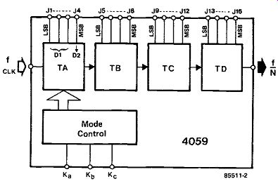
The excellent properties of counter/divider IC type 4059 have, so far, not been given the prominence in Elektor Electronics they deserve. One of these properties is the provision of divide ratios anywhere between 3 and 15 999 depending on the logic level at inputs Ii ..uis and the setting of switches S17.. .S19.
The 4059 is clocked by a relaxation oscillator, N1, N2, which could have been a crystal-controlled type instead of the one shown in figure 1.
The dual-D bistable type 4013 at the output is essential because the width of the pulses at pin 23 of the 4059 is comparable to the clock frequency.
The bistable ensures that the pulses emanating from pin 23 are reshaped into rectangular form. The ohm output of the bistable is, of course, half the frequency of the wave train at pin 23 of the divider.
Inputs J1 ... J16 of IC2 are divided into groups of four. The binary information at these inputs is called TA . . To. Inputs J1...J4 are further sub divided into D1 and D2. In total there are, therefore, five data inputs, of which the smallest, D2, is only one bit wide. Furthermore, the 4059 has three mode control inputs, Ka...Kc, whose composition results in a factor K as shown in table 1. If K =10, input D1 becomes four bits wide: J4 then forms part of D1! The divisor, n, is then calculated from:
n = 103TD + 102Tc + 10Ts + D1
In all other cases,
n =K(10^3 2 + 10^2 TD +10Tc + TB)+ D1
---------
The 4059 can be Programmed by computer, by hand, or with the aid of an up-or-down counter.
The generator can be used in electro-phonics, in measuring techniques, as timer, and even as a digital phase-locked loop frequency synthesizer in FM tuners.
The circuit operates from a 4 .. .15 V supply and current consumption is small.
288 RMS-TO-DC CONVERTER
For some obscure reason, establishing the root-mean-square (rms) value of an alternating voltage seems to be among the least familiar procedures for many an electronics hobbyist; measuring the alternating voltage may be easy, but deciding on the relevant unit expressing quantity- rms, mean, or peak-to-peak value- is quite another matter.
Since the rms value of an alternating voltage is the most frequently used of the above mentioned three, some convenient means of obtaining that value without calculations may be of interest in practical measuring techniques.
The rms value of an alternating voltage U across a resistor R equals the direct voltage causing the same dissipation level in R.
Example: a 50% duty factor, 1 Vpp rectangular voltage across a resistor R. Find the rms level of this voltage.
The mean dissipation in R, caused by this periodic signal equals rz (Upp)2/R = 1/(2R) [W]
The direct voltage causing the same dissipation has a level of %1/2 V, since P = (Y2 I/2)2/R = 1/(2R)[W].
-------------
This is also the conversion factor for obtaining the rms value from the peak-to-peak value, since
Urms = IMUpp2 = 1/2 Upp 0.71Upp[V]
therefore Upp 1.4IUrms in this example.
Although moving coil meters measure the mean value of the rectified (pulsating) input voltage, they are calibrated in terms of rms voltages. Therefore, the calibration is only valid for sinusoidal voltages.
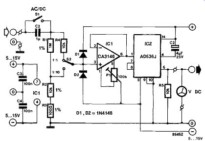
The proposed rms-to-DC converter is a relatively simple circuit as it incorporates a dedicated chip, the Type AD536 by Analog Devices. Alternating voltages applied to input terminal 1 are proportionally converted into a direct output current, which causes a direct output voltage across an internal 25 k-ohms precision resistor; a buffer opamp outputs the direct voltage equivalent (i.e. rms value) of the input alternating voltage.
IC1 functions as an input buffer in view of the relatively low input impedance of the rms converter chip. The maximum permissible peak-to-peak value of the input voltage to the Type AD536 equals the symmetrical supply voltage level; D1 and D2 have been added to protect IC1 against accepting input voltage levels in excess of the ± supply voltage. S2 functions as a x 1/ x 10 input attenuation selector to enable high voltage measurements; the function of S1 is to block any DC components in the input signal to the converter. It is useful to realize that the rms value of a composite (AC + DC) signal is calculated from Urrns = j/UDC'-l- UAC2.
Preset P1 should be turned to obtain 0 V with respect to ground at terminal 6 of IC2 with no input signal applied and S2 set to the x1 position.
The converter achieves an accuracy of 1% for input voltage levels lower than 100 mV and input frequencies up to about 6 kHz. For signals up to 1 V, the bandwidth is expected to be of the order of 40 kHz, while 100 kHz may be attained with input voltages above the 1 V level. Current consumption of the circuit is about 5 mA.
Parts list
Resistors:
R1 =1M;1%
R2= 10k;1 %
R3 = 100 ohm ;1% R4,R5 = 10k P1 =100k preset
Capacitors:
C1 =4.7/.4;25 V electrolytic
C2 =1µ;MKT
C3;C4= 100n
Semiconductors:
D1;D2=1N4148
IC1 =CA3140
IC2 =AD536J
Miscellaneous:
S1 = miniature switch
S2= toggle switch
PCB Type 86462
289 SERVO-MOTOR TESTER
----------
This circuit is of interest to two categories of readers; first, model aircraft/boat/train enthusiasts objecting to having to leave their radio control transmitter switched on for extended periods in order that a servo-motor and associated mechanical parts can be made to function as desired; secondly, constructors of computer-controlled robots incorporating servo-motors. The latter field of interest is a typical combination of mechanics and electronics plus software, and it is sometimes urgently required to be able to keep them apart as the specific parts of the robot have been prepared for testing, which, arguably, should be possible to do without having to write special programs to this end on the computer.
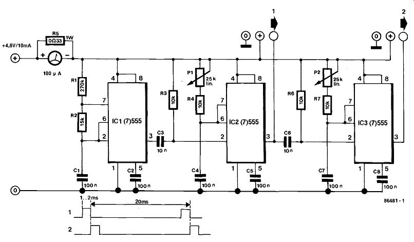
The proposed servo-motor test unit is, as can be seen from the circuit diagram, a downright simple design based on the use of Type 555 or 7555 timer chips connected in a cascade arrangement which can be expanded further to drive more than two servos at a time, if desired; it is readily seen that the second and third stages of the circuit are identical.
The first timer, IC1, serves as an astable multivibrator whose output pulse period time is determined with T= 0.693(R R2)C. The indicated values for the relevant timing parts therefore provide a pulse period time of about 20 ms at pin 3 of IC1. The rising edge of this square wave triggers monostable IC2, whose output pulse width may be set with Pi; the given series connection of Pt and R4 ensures a large enough pulse width range for most types of servo-motor, which typically require activation pulse widths of the order of 1...2 ms.
The second servo control stage is identical to the set-up around IC2, and up to eight triggered 555 stages, each with its own pulse width control, may be cascaded in this way.
It is suggested to fit each of the servo control potentiometers with a simple scale in order to have a relative indication regarding the motor's lateral or angular position.
The ammeter in series with the positive supply line offers an indication about the total current consumption of the servos, and it is thus readily detected when one or more have got stuck in their movement. The test circuit itself does not con tribute much to the total current consumption indicated on the meter; some 3 mA is required for each Type 555 timer in the row, while the use of low power Type 7555 equivalents should reduce this figure even further. It is, therefore, perfectly feasible to make the tester into a portable, battery-operated unit, powered by four penlight type NiCd batteries.
290 SIMPLE SWEEP GENERATOR
The sweep generator is an indispensable piece of measuring equipment for testing the frequency response of AF amplifiers, filters, and loudspeaker systems. At the heart of this design is the well known Type XR2206 function generator chip from EXAR. It is seen to the right on the circuit diagram, in a standard application with 3 capacitors and a rotary switch for selecting the frequency range, and a potentiometer, P5, for adjusting the amplitude of the output signal. The signal frequency is a function of the current drawn from pin 7 on the XR2206:
f0= 320 I/C [Hz]
... where I is in milli-amperes, and C is in micro-farads.
It should be noted that pin 7 is internally kept at 3 V, which is available at pin 10 also.
The left-hand part of the circuit comprises the sawtooth generator, IC1, and a buffer, IC2. The former is set up as an integrator, whose sweep period depends on the voltage at terminal C. Potentiometer P2 enables setting the sweep period between 0.01 and 10 seconds; the maximum duration is adjusted with P4. The sawtooth voltage at pin 6 of IC, has an amplitude of 5 Vpp, and can be used to drive the horizontal deflection 1X1 input of an oscilloscope via terminal K. The amplitude of the sawtooth voltage is determined by the zener voltage of D1 and the base-emitter voltage of Tz, which is briefly turned off when the output of IC, exceeds 5 V. The collector of this transistor is then pulled to ground via R3, so that T1 is switched into conduction. The integrator is reset by making the- input of IC1 positive with respect to the + input with the aid of T3, R5 and Re.
Capacitor C1 serves to lengthen the on-time for T1 and T3 to ensure that the flyback of the sawtooth is finished.
Potentiometer P1 is a voltage divider to define the sawtooth amplitude, and hence the sweep range, while S1 makes it possible to turn off the sweep function (position F).
Opamp IC2 is configured as a buffer stage for inverting and attenuating the sawtooth voltage, to which a direct voltage is added also. The output of IC2 carries a sawtooth voltage with an amplitude between 0 and 2.85 V, or a direct voltage between the same limits when S1 is set to position F. Bearing in mind that the reference voltage of IC3 is 3 V, the current through R13, and hence the output frequency, can be varied by a factor 20, which is the maximum attainable deviation factor in all 3 frequency ranges. The frequency scale can be calibrated with the aid of P3.

-----------
Parts list:
Resistors (±5%):
R1 =22K
R2;R4;R17=10K
R3 = 4K7
R5 = 1K2
R6 = 10 R
Miscellaneous:
S1 = miniature SPDT switch.
S2= miniature SPST switch.
R7 = 1 MO
R8 = 68K
R9;R10 = 820K
R11;R12 = 470K
R13 = 2K2
R14, R15 = 33K
R16= 220R
P1= 50K linear potentiometer
P2 = 100K linear potentiometer
P3 = 100K preset
P4 =100R preset
P5 = 1k0 logarithmic potentiometer
Capacitors:
C1 =3n3
C2=12n
C3 = 68p
Ca =1µ; 16 V; radial
C6=22n C6 = 220n
C7 = 2µ2; 16 V; radial
C8 = 10µ; 16 V; radial
C9 = 2n2
C10=220µ; 16 V; radial
C11;C12=100n
Semiconductors:
D1 =zener diode 5V6; 400 mW
T1;T2 = BC557
T3 = BS250 IC3;IC2= CA3140
IC3= XR2206 S3 = 1 pole, 3-way rotary switch.
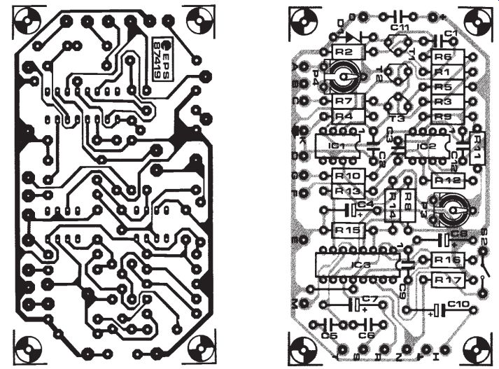
PCB Type EPS87419
----------
291 SIMPLIFIED WORD COMPARATOR
Primarily intended as a trigger source for an oscilloscope in the testing of digital circuits, the comparator is a derivative of the word recognizer and delayed trigger published in the July/August 1981 issue of Elektor Electronics.
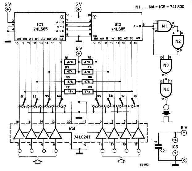
When an 8-bit binary word is recognized during a comparison with a pre-determined value, the present circuit issues a short trigger pulse. In contrast to the original circuit, the present one has no provision for either a delayed trigger pulse or an external trigger input. None the less, the comparator remains an almost indispensable aid in the testing of digital circuits.
The unit is based on two four-bit comparators, IC, and IC2. The reference level for them can be set separately with switches S1 . . . S4 and S5 . . . S8 respectively. With these switches set as drawn, inputs A and B are interconnected: this is the don't care position. With a switch set to its center position, a high reference level is obtained, while when it is set to the extreme right position, a low reference level is obtained.
When all A and B inputs agree, the A = B output of IC2 goes logic high. Gates N, . .N4 suppress short spurious pulses that arise during the stabilization of the comparator inputs.
The size of the binary word can be increased by cascading two or more comparators. Account must then be taken of the transit delay which amounts to 24 ns per comparator. In some tests this may lead to an unacceptable delay if several comparators are used.
The current consumption is about 60 mA per comparator: 32 mA is drawn by the LS241, and 10 mA by the LS85. This enables the current consumption of multiple comparators to be calculated quite easily.
Note that each additional IC must be separately decoupled by a 100 n capacitor.
-------------
292 TWO-TONE RF TEST OSCILLATOR
This test oscillator is useful to ensure optimum operation of RF amplifier stages designed to work on the short-wave bands. Based on two crystal oscillators, it provides considerable output power (10 to 100 mW) to enable measuring intermodulation characteristics of high level and RF power stages.
The quartz crystals used here not only serve as the frequency determining elements (2 ... 20 MHz), but also as output filters to prevent one generated signal being lost in the other oscillator. With this in mind, tapped inductors L1 and L2 ensure freedom of mutual interference when the oscillator is used for frequencies higher than 10 MHz. Both inductors are wound as 12 turns of enameled copper wire with a center tap, on either a small balun or a suitably rated core with an air gap. Outputs of equal amplitude can be obtained by adjusting P1.
The test oscillator consumes about 250 mA from a 60 V supply. This means that both transistors should be fitted with a heat-sink, and that chokes L3 and L4 should be capable of carrying about 150 mA.
293 VARIABLE WIEN BRIDGE OSCILLATOR

-----
A Wien bridge oscillator can be made variable by using two frequency determining parts that are varied simultaneously at high tracking accuracy.
High-quality tracking potentiometers or variable capacitors are, however, expensive and difficult to obtain. To avoid having to use such a component, this oscillator was designed to operate with a single potentiometer. The output frequency, fo, is calculated from f0=1/(2TiRCl/a) where R = R2 = R3 = R4-= R6, C = C1 = C2 , and a=(P1+R1)R. Preset P2 allows adjusting the overall amplification such that the output signal has a reasonably stable amplitude (3.5 Vpp max.) over the entire frequency range.
The stated components allow the frequency to be adjusted between 350 Hz and 3.5 kHz. Other frequency ranges are readily defined with the aid of the above formula, although it should be noted that the upper frequency limit is determined mainly by the gain-bandwidth product of the opamps Type OP-221 and TLC272. The current consumption of the oscillator depends on the type of opamp used.
The following values were measured: OP-221:
0.5 mA; TLC272: 2 mA; TL072: 2 mA.
The construction of the oscillator should present very few problems since a ready-made circuit board is available.
(PMI Application)
Parts list
R1=10K R2;R3;R4;R6=100K R5=2M2
P1 = 1 MO linear potentiometer
P2=5k0 preset
Capacitors:
C1;C2=1n5
C3;C4 = 100n
Semiconductors:
Di:D2=1N4148 IC, =TLC272 or TL072 or OP-221
Resistors (±5%):
Miscellaneous:
PCB Type 87441

-------
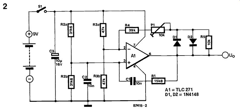
294 WIEN BRIDGE OSCILLATOR
This AF oscillator can be built with only one active component, and draws so little current that it is conveniently fed from a 9 V (PP3) battery.
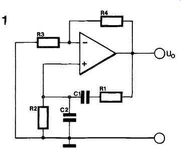
The basic circuit of the Wien bridge oscillator is shown in Fig. I. The oscillator consists of two sections, namely the opamp plus R3-R4 which deter mine the amplification factor, and positive feedback network C1-R1-C2-R2 which enables the circuit to oscillate. This network is composed of a low-pass section R2//C2, and a high pass section R1 +C1.
The phase difference incurred in these is nulled at the frequency of oscillation, when the filters form a pure ohmic potential divider with an attenuation of
3. Therefore, the opamp must have an amplification of 3, to keep the overall amplification at unity, so that the oscillation is maintained. The output frequency, f0, of the oscillator is f0= 1/(2 pi I/R1 R2 C1 C2) [Hz]
... but only if R1 = R2 and C1 = C2. In the practical design shown in Fig. 2, the oscillation frequency is about 1,000 Hz.
Both the inverting and the inverting input of the opamp in Fig. 1 must be held at half the supply voltage to ensure minimum current consumption if the oscillator is to be fed from a battery. Figure 2 shows how this is realized in the practical version of the Wien bridge oscillator. Here, resistors R2 and R3 from Fig. 1 are seen as R2a-R2b and R3a-R3b, respectively, connected as voltage dividers. This can be done with impunity, because the voltage source is a virtual short circuit for alternating voltages, and there is also C3 as an effective decoupling device.
For an alternating voltage, therefore, the resistors are parallel combinations. Evidently, R2a, R2b, R3a, and R3b have two times the calculated resistance of the respective components R2 and R3 in Fig. 1.
The amplification of the opamp is adjustable with P1, which should be set for reliable oscillation at virtually no distortion of the output sine wave.
When the oscillator is properly aligned, the distortion should be less than 0.1%.
The use of the Type TIC271 CMOS operational amplifier results in a current consumption of only 0.32 mA at U.=6 V... It is possible to use a special low-power opamp such as the type OP-22 biased with a resistance of 1 M ohm to reduce the current consumption to 0.1 mA. However, this will cause the oscillation frequency to be limited to 1,000 Hz, due to the reduced slew rate at very low bias settings, which in turn give rise to a strong increase in the distortion level.
PMI Application Note ABM.
-------
-------