Here is an all-purpose d.c. power supply for symmetrical as well as asymmetrical use, and capable of supplying high output currents and voltages. An all-analog design based on discrete parts only, this 400-watt PSU deserves a prominent place on your work bench.
by G. Boddington
---------
MAIN SPECIFICATIONS
• Mode: Single
- one adjustable power supply with current and voltage controls.
- Output: 0 - 40 V at 0 - 5 A
• Mode: Independent
- two identical, electrically separated, power supplies.
- Outputs: 2 < 0 -4 0 Vat 2 x 0 - 5 A
• Mode: Tracking two identical, series connected, power supplies.
Outputs: ±0 -± 40 V at 0 -5 A 0 - 80 V at 0 - 5 A
Voltage and current of slave follow master.
• Mode: Parallel
- two identical, parallel connected, power supplies.
- Outputs: 0.6 - 39.4 V at 0 - 10 A
• Maximum output voltage:
40 V (at full load)
48 V (no load)
• Maximum output current: 5 A
• Ripple:
10 mV (no load)
50 mV (at full load)
• Voltage difference in tracking mode:
50 mV
---------

The problem with power supplies in an electronics laboratory or workshop is that their application range is often limited because of their specifications. Any one who has been involved in practical electronics will admit that finding a suitable power supply for a particular test is not at all easy, when none of the available ones (say ±15 V/2 A, 0 60 V/100 mA and 5 V/10 A types) seem to be fully geared to the job. Obviously, what is needed is a supply that combines the most frequently used voltage and current ratings, both symmetrical and asymmetrical, while offering a properly operating overload protection.
Although the user manual with many an inexpensive, ready-made power supply will confidently inform you that the power transistors are protected against overloads, this type of protection has an inherent disadvantage. True, the supply will happily supply the maximum output current at the maximum output voltage, but it will typically shut down the moment the voltage is reduced just one volt or so. The reason is clear: the over load protection is actuated because the extra dissipation, which is the product of the output current and the voltage difference across the series transistors, exceeds the cooling capacity of the heat-sink, or the power rating of the (expensive) series transistors.
The present power supply puts an end to these problems. It can be set up to supply either 2 x 40 V/2 x 0 - 5 A, ±0 - 40 V/0 - 5 A, or 0 - 80 V/0 - 5 A, and is capable of supplying the maximum output current at low voltage settings. Special ICs or micro processors are not used: just straightforward analogue electronics based on readily avail able components. The result is a power supply with an excellent price/performance ratio.
Block diagram
The instrument consists of two identical, electrically isolated, power supplies, which may be connected in a number of ways to give different operating modes. The block diagram in Fig. 1 shows relatively many functional blocks, which together form three partly 'interwoven' regulating circuits. The first of these, the outer circuit, is a transformer preregulator that serves to keep the voltage drop across the series transistors (T4-Ts) constant at about 10V, so that the maximum dissipation remains smaller than 50 W (or 25 W per transistor). The other two regulation circuits are for the output voltage (U) and current (I). These circuits are almost identical, the only difference being that the current control obtains its control information from a series resistor, and the voltage control from a potential divider fitted across the output terminals. In contrast to the trans former preregulation, the U and / control circuits allow the range of the regulating action to be adjusted manually. Interestingly, the series transistors, T4 and Ts, function in all three regulation circuits.
The block diagram shows a second power supply, which provides auxiliary ±12 V rails for use in the main circuit. The ground line of this symmetrical supply is connected to the positive output terminal of the main supply. This means that all references to '+12 V' and '-12 V' in the following text, and in the circuit diagram, are actually '+12 V and -12 V with reference to the positive output terminal'. The auxiliary power supply also functions as a voltage reference.
Finally, the block marked 'current limit' stands for a circuit that keeps the output current of each supply below 5 A. This circuit may be fitted with an optional temperature monitor to prevent overheating.
The preregulation circuit
The basic operation of the preregulation circuit is best explained with reference to Fig. 2.
The current flows from the positive connection of the bridge rectifier to the positive output terminal via two parallel-connected darlington transistors, T4 and Ts, and resistors R13, R14 and R18. The regulation circuit tries to maintain a constant drop of 10 V across the series transistors and their emitter resistors. Transistor T3 is driven via potential divider Rts-R16 and network C24-R17. The network introduces a small delay to eliminate the effect of noise spikes in the preregulation. The current through the LED in optocoupler ICs is inversely proportional to the voltage across R15-R16.

Fig. 1. Block diagram of the power supply. The design is based on three
interactive control circuits: (1) transformer preregulation, (2) current
control and (3) voltage control.
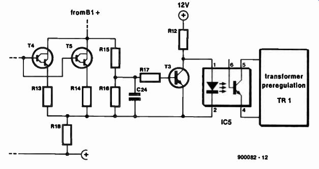
Fig. 2. Basic diagram of the circuit that controls the transformer preregulation.
The power fed to mains-connected ohmic loads is relatively simple to control. Usually, an adjustable R-C network connected across the mains terminals supplies the trigger voltage for a triac. The timing of the trigger (or firing-) pulse with respect to the start of the half-cycle is determined by the R-C delay.
After being fired, the triac conducts until the mains voltage drops to a level below the minimum hold current. This happens close to the zero-crossing. The triac remains blocked until it receives another trigger pulse at a particular phase angle during the next half-cycle of the mains voltage. The current supplied to the load is inversely related to the phase angle, i.e., to the delay of the trigger pulse following the zero-crossing. This principle of phase-angle control works as long as voltage and current are in phase, i.e., as long as the load is a pure resistance.
Unfortunately, the mains transformer in the power supply forms an inductive rather than an ohmic load, so that the mains voltage and the load current are out of phase. Hence, a simple 'dimmer' with conventional triac control as described above will not do as a preregulation circuit. With an inductive
load, it may happen that although the instantaneous voltage is high enough to fire the triac, there is no current to 'hold' the device.
Therefore, the firing may take place only when the load current is sufficiently high to keep the triac conductive. However, since the load current in a power supply is variable, the phase shift between voltage and current is also variable. This means that the width of the trigger pulse rather than the position must be controlled. If the pulse were simply shifted, the result would be an asymmetrical output current with a high d.c. component, causing rapid saturation of the transformer winding. When the pulse is stretched, however, due care must be taken to prevent it from extending over the zero crossing of the mains voltage.
The circuit section in Fig. 3 stretches the first pulse by means of pulse sequence triggering, an approach which is particularly suited to applications with load currents that are prone to variation. The R-C network connected between the live and neutral lines of the mains serves to delay the trigger instant.
The network consists of C1, potential divider R29-P1-R30 (branch 1), series resistor R31 and bridge rectifier D20-D23 (branch 2). The combination of the bridge rectifier and the opto coupler it powers simply forms an adjustable resistor for alternating voltages, so that both branches have the same function: making the trigger delay, cp, variable (see Fig. 4a). The basic delay is determined by Pi.
When the power supply is switched on, C1 is charged. When the trip voltage of the diac is reached, both D11 and Tr11 are fired.
When a trigger current flows from C1 to Tr11, resistor R32 drops a voltage which is high enough to trigger a smaller triac, Tri2. The result is that the discharge time is no longer determined by the two branches, but by (R33+R29)0. When C1 can no longer supply the hold current for Tr12-which happens fairly quickly because of the small resistors R33 and R29-the triac blocks and C1 charges again. This sequence is repeated until just be fore the zero-crossing, when the mains voltage can no longer charge C1 (see Fig. 4a). The waveform across the thyristor is shown as a dashed line in Fig. 4b. Figure 4c, finally, shows the waveform of the current shifted by an angle cp as a dashed line, and the wave form produced by the dimmer as a solid line.
Asymmetry of the waveform occurs during the first half-cycle only. The triac conducts up to instant 'B', when the load current falls to zero.
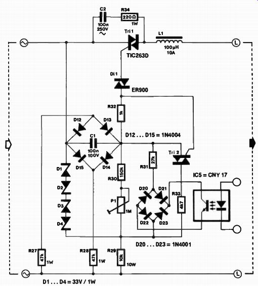
Fig. 3. Circuit diagram of the transformer dimmer. The trigger delay is
controlled by the circuit in Fig. 2 via an optocoupler, IC5, and an adjustable
bridge rectifier, D20-D23.

The function of the remaining parts in this section of the circuit is quickly explained: the zener diodes limit the voltage across Tri2 to about 66 V whilst providing a stable reference voltage for the trigger circuit. Components D12, D13, D14, R27 and R28 ensure that C1 discharges during the zero crossing. Inductor Li serves to eliminate current surges and thus prevent HF interference. Network C2-R34 short-circuits spikes generated by the switching sequences, and so prevents erroneous triggering.
Voltage and current control
The operation of the voltage control circuit is illustrated in Fig. 5. Potential divider P3-R9 allows a reference voltage of 0 to -10 V to be set between ground (the positive output terminal) and -12 V. A second potential divider, R7-R8, at the output terminals sup plies about 20% of the output voltage, i.e., about 0 to -9 V (with respect to the positive output terminal). The voltages supplied by the two potential dividers are compared by opamp IC4, which, with the aid of T4-T5, will attempt to keep the voltage difference between its two inputs as small as possible.
When a higher output voltage is required, the wiper of potentiometer P3 is turned to wards the -12 V potential. The voltage at the non-inverting input of IC4 drops, so that the output voltage of the opamp rises. Conversely, when a lower output voltage is set either by the user turning P3, or by the actuation of the voltage limiting circuit, the inverting input is at a higher potential than the non-inverting input, so that the opamp output voltage drops.
The current control circuit (Fig. 6) operates in a similar manner. Like IC4, opamp IC3 will attempt to keep its output voltage at 0V. The main difference with the voltage control circuit, however, is that the reference voltage for the opamp (applied to the non-inverting input) is permanently grounded via Ri, while the current is measured as the drop (max. 1.1 V) across series resistor R18. Potential divider P2-R3 is arranged so that its junction carries a voltage between -1.1 V and +1.1 V with respect to the positive output terminal. When no current flows through R18, the positive side of P2 is at ground potential.
When P2 is advanced to the 5-A position, i.e., to its full resistance of 2.2 1(12, the inverting input of IC3 is at a voltage of -1.1 V. Consequently, the voltage at the opamp output rises.
When a current of 5 A flows, R18 supplies 1.1 V. When P2 is turned to the other extreme position (i.e., a resistance of 0 ohms), the voltage at the inverting input is higher than that at the non-inverting input, so that the opamp output voltage drops.
As shown by Figs. 5 and 6, and also by the complete circuit diagram in Fig. 7, the an odes of D8 and D24 share a common connection, R23, where the opamp outputs of the current and voltage control circuits are joined. This means that the opamp that sup plies the lower output voltage determines the base voltage of the current booster, T4-TS. Resistor R23 serves to hold the bases of T4-T5 at about +11.5 V. Diodes D7 and D9 decouple the opamp outputs, preventing current from flowing between them. One of the series connected LEDs lights when the voltage at the associated opamp output drops to a level below 1 1.5 V minus two diode voltages (D24 D7 or D8-D9). This happens when the relevant limiter (current or voltage) starts to operate.
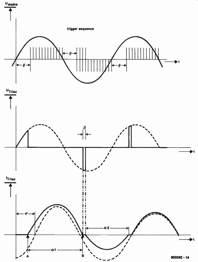
Fig. 4. Illustrating the basic operation of the dimmer for inductive loads,
applied here for the purpose of transformer preregulation. Fig. 4a shows
the position of the trigger pulses with respect to the mains voltage. The
voltage across triac Tri1 as compared to the mains voltage (dashed line)
is shown in Fig. 4b. Fig.4c, finally, shows the current shifted by an amount
of cp, without (dashed line) and with (solid line) phase angle control.
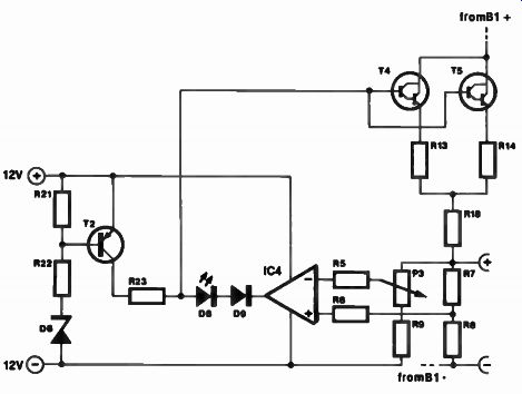
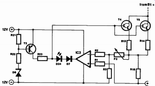
Fig. 5. Basic voltage control circuit. Fig. 6. Basic current control circuit.

Fig. 7. Circuit diagram of the laboratory power supply. Two of these circuits
are required for the parallel, series and symmetrical modes.
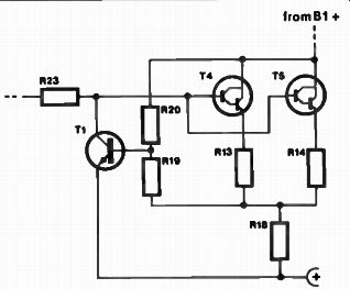
Fig. 8. Basic layout of the current limiter.
During the switching-on sequence the circuit around T2 keeps the series transistors off until the zener voltage of D6 is reached.
This happens when the negative supply voltage of the opamp is sufficiently high. In this way, the voltage peak at switch-on is limited to about 2.5 V above the set output voltage, which is available after a few milli seconds. Although the switch-on peak is not likely to cause damage to most equipment powered by the supply, it is recommended to first switch on the PSU and then connect the load.
The current limiting function of the PSU is provided by the circuit in Fig. 8. As long as the pre-regulation circuit operates correctly, there exists a constant voltage difference across T4-R13 and Ts-R14. In a fault condition of any kind (overcurrent, overvoltage), Ti i switched on via potential divider 1219-R20.
This reduces the base voltage of the darling ton transistors, so that the output current i limited. To implement a combined current/ temperature overload function, replace resistor R20 by a 100-1d2 NTC (negative temperature coefficient) resistor which is bolted on to the heat-sink, close to T4-T5.
Also see: Medium Power A.F. Amplifier