by T. Giffard
For the many readers who do not need hundreds of watts output from their audio hi-fi installation here is a modest 60-watt a.f. amplifier that is a match for even the best quality loudspeakers. Loads down to 2 ohms may be driven without any problem and with very low distortion. The design is entirely symmetrical and, apart from an input capacitor, direct coupled.
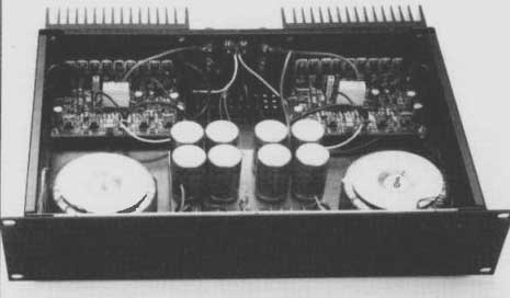
WHAT should be the power rating of a domestic hi-fi installation? Twenty watt, 50 watt, 200 watt? It is a vexed question that will never be answered to the satisfaction of every hi-fi buff. Psychology may play a role here, too: the difference in sound pressure between a 20-watt and a 200-watt system is only (!) 10 dB and that sounds a lot less than the difference of 180 watt in output powers. Be that as it may, a continuous power of 50-70 watt is more than adequate for at least 95% of all domestic hi-fi installations.
It's far better to have a good quality 50-watt system than a mediocre 200-watt one. Readers who take music reproduction seriously will, no doubt, have found this out themselves a long time ago. Having said that, it is admitted that there are a few, and fortunately only a few, loudspeakers that need at least a hundred watts to come to live.
Go to almost any hi-fi retailer and ask for a good-quality, medium power (say, 50 W) amplifier and you'll find that there are not many, if any. Until recently, the quality of almost all proprietary power amplifiers was in direct proportion to their power rating and that is the reason that many people buy a sys tern with too high a power output for their requirements.
Fortunately, some clever manufacturers have realized this anomaly and are doing some thing about it, so that amplifiers rated at 50-70 watt with a good specification are slowly becoming available. Nevertheless, we felt that a good-quality design for the enthusiastic DIY-er would be a welcome addition to the couple of high-quality preamplifiers we have published over the past few years.
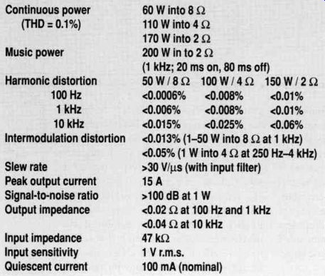
---------- TECHNICAL DATA
Power supply 225 VA; buffer capacitor 20 000 uF per line
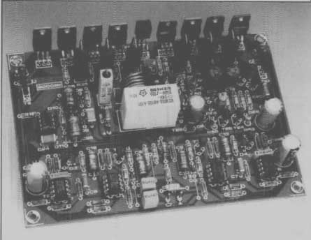
Symmetrical design
Top priority in the design of the amplifier was quality, and this has resulted in a unit with a signal-to-noise ratio of not less than 100 dB at 1 W, harmonic distortion of not greater than 0.006% (8 ohm /50 W) and a slew rate of 30 V /u-s.
If you imagine a horizontal line through the centre of the simplified circuit diagram in Fig. 1, the part above that line is a mirror image of that below the line (ignoring the DC correction and protection circuits). The active DC correction circuit ensures that in no circum stances will direct voltage appear at the output, which is important in view of the direct coupling between all stages.
The protection circuit provides a delay on power-on, monitors whether there is any direct voltage at the output, and measures the current that is drawn by the output transistors.
A mechanical relay is used, because we could not devise an electronic switching method that would satisfactorily limit the current without audible side-effects.
Although the design cannot be called revolutionary, we feel that parts of it are pretty original and combine some of the advantages of a number of other, standard designs.
The open-loop gain has been kept low, so that the amount of feedback can be kept small, which is all to the good of the overall quality. After all, the various stages then need contribute a smaller part of the overall amplification, which helps in keeping the distortion in each stage very small.
The input is formed by a differential amplifier, T1–T5, whose gain is limited to about 40 dB. The input transistors are coupled to another pair of differential amplifiers, T2 and T6 respectively, whose gain is about 27 dB. These are followed by controlled current sources T9 and T10. Setting of the quiescent current for the output stages is provided by a vari able zener diode consisting of three transistors, which are connected between the collectors of T9 and T10.
The output stages consist of drivers T13 and T17, and two pairs of three parallel-connected power transistors, each forming a super emitter follower.
Choice of components
In a symmetrical design, equality of the transistors in the input stages is of paramount importance. In our first design, self-paired BC transistors were tried, but these gave problems, particularly with thermal stability. It was therefore decided to use proprietary dual transistors, although these are rather more expensive. However, taking into account the necessary reliability of reproduction of the design, and looking at the near perfect parallel operation of the dual transistors and their excellent thermal behavior, the expense is well worth it.
Some of the problems a designer often has to cope with are concerned with the avail ability of components. The output transistors in the present design are a typical example.
Although they were listed as standard types in a Philips catalogue, the ones we ordered had not been delivered six months later in spite of numerous telephone calls. Perhaps this explains why Philips has not been doing too well of late. In the end, the order was can celled and replaced by one for SGS-Thomson devices (delivered in a few weeks). These are in most respects as good as the Philips types but lack somewhat in bandwidth, although in the prototypes that was not noticeable. On the other hand, the characteristics of the complementary n-p-n and p-n-p types are for all practical purposes identical.

Fig. 1. The simplified circuit diagram of the amplifier clearly shows the
symmetrical design.
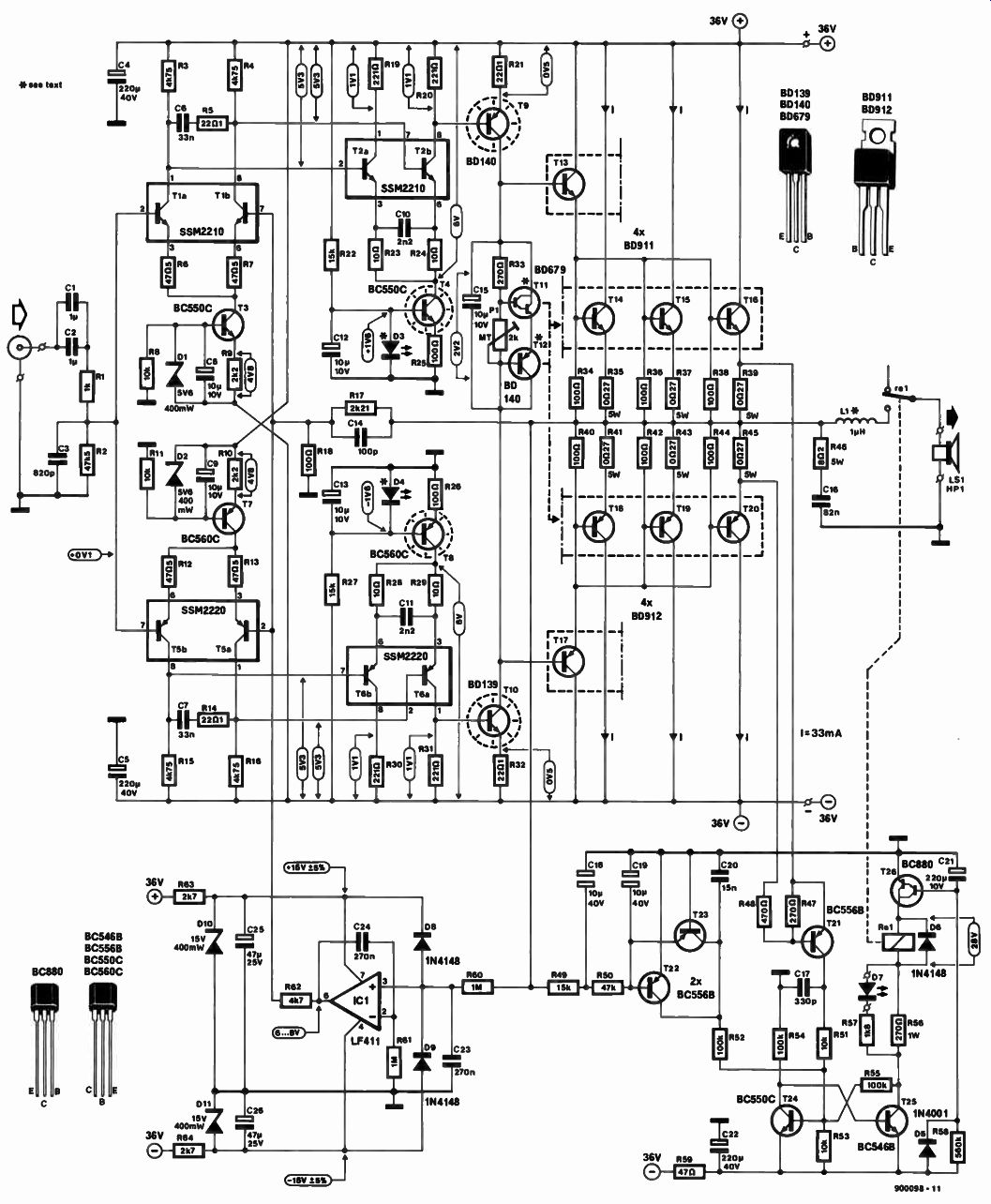
Fig. 2. Circuit diagram of the medium-power A.F. amplifier.
The final design
The input of the amplifier-see Fig. 2-is protected against direct voltages by capacitors 0 and C2, which may be omitted if the preamplifier to be used already has a capacitor at its output. Be careful in future when connecting a different preamplifier which may not have a capacitor at its output.
The input capacitors are followed by a low-pass filter, R1 C3. This network limits the bandwidth of the input signal to obviate any transient intermodulation distortion (Tim). The cut off frequency of the filter is about 180 kHz, assuming that the output impedance of the preamplifier is 50 Dual transistors Ti and Ts form the sym metrical input stage, which is controlled by current sources T3 and T7. The current through each of the dual transistors is set at just above 1 mA. The gain of the differential input amplifiers is determined by the ratio of the values of their collector and emitter resistors. Networks R5-C6 and R14-C7 set the open-loop bandwidth at 500 Hz.
The second stage consists of dual transistors T2 and T6, which are controlled by current sources T4 and Ts. This stage not only provides 27 dB gain, but also impedance matching between the input stage and the following current amplifier.
Current sources T4 and Ts use LEDs to obtain a voltage reference. Bear in mind that these diodes have a potential drop of about 1.6 V across them.
The quiescent current through current amplifiers T9 and T10 is some 20 mA. This level of current is necessary to ensure that drivers T13 and T17 provide sufficient current in all circumstances. The amplification of these amplifiers is determined by the value of their emitter resistors and the input impedance of T13 and T17.
The collectors of the current amplifiers are inter-coupled via a pre-settable 'zener' network, which serves to set the quiescent operating point of the output stages. This net work normally consists of just one transistor, but it was found that the thermal behavior of this was not sufficient to compensate the thermal conduct of the output stages correctly and quickly enough. The three transistors finally chosen work almost perfectly and have the further advantage that they form a virtually ideal current source which ensures that current variations through them hardly affect the zener voltage.
The drivers and associated power transistors are, of course, of the same type. Three output transistors instead of one make for more efficient cooling; moreover, low-power transistors normally have better electrical properties than high-power ones.
A Boucherot-type network, R46-C16, at the output ensures that the amplifier remains adequately loaded at high frequencies.
Inductor L1 limits the rise time of the output signal when the load is capacitive. This results in slightly less damping at high frequencies, but even so the damping factor at 10 kHz and an output impedance of 8 ohm remains greater than 100. Feedback is provided via resistors R17 and R18, and an important role in this is played by DC correction circuit IC1. Since the feedback loop does not include coupling capacitors, direct voltages at the input are amplified to the same degree as AC signals.
Owing to the slightly asymmetric setting of the direct voltages at the differential input stages, which is unavoidable because of differences between n-p-n and p-n-p transistors and also in base resistance, it is essential that the output voltage of the amplifier is kept at 0 V, and this is effected by IC1.
The output of the amplifier is applied to integrator IC1 via low-pass filter R60-C23. The supply for the integrator is derived from the main 36-V supply with the aid of resistors R63 and R64, and zener diodes D10 and D11.
The protection circuit is formed by transistors T21-T26. When the supply is switched on, T26 is off, so that bistable T24-T25 is reset, which results in T25 being switched on.
Transistor T26 cannot conduct until its base emitter voltage is high enough and this does not happen until C21 has been charged via R58. It is this action that delays the actuation of the amplifier.
Once T26 is switched on, relay Re1 is energized and diode 137 lights to indicate that all is well.
Transistor T21 monitors the output current of the amplifier by measuring the potential drop across the emitter resistors of T16 and T20 via voltage divider R47-R48. If that current exceeds 5A (that is, a total current through the three output transistors of 15 A), T21 switches on which results in bistable T24 T25 toggling after which the relay is deenergized within 5 ms.
Any direct voltage at the output is measured via low-pass filter R49-R50-C18-C19. If there is a direct voltage at a level of more than 1 V, T22 will switch on of the voltage is negative and T23 if it is positive. Again, the relay is deenergized via the bistable.
When the relay is de-energized owing to too high a current or voltage, it will remain so until the supply is switched off. When, after a few seconds, the supply is switched on again, the relay will be energized if the fault condition has been removed.
The nominal supply voltage is 2x30 V, which may rise under no-load conditions to 2x37 V. Each amplifier may have its own power supply, but it is, of course, possible to power a stereo system (two amplifiers) from one supply only as discussed below.
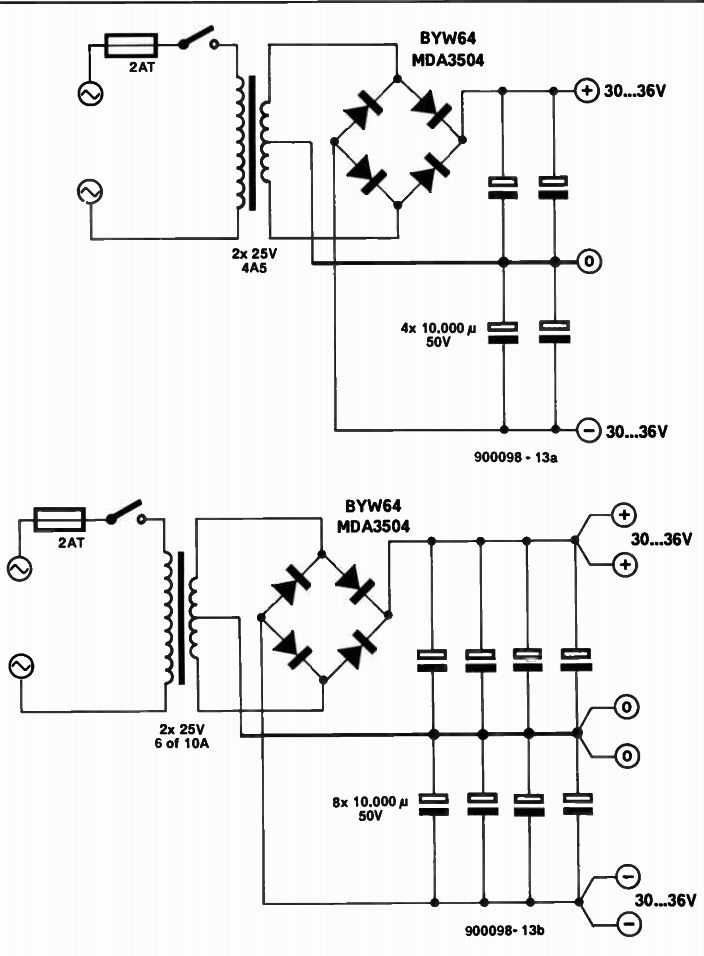
Fig. 3. Two possible power supplies: the one at the top is for a monaural
amplifier, while the one below is a single supply intended for a stereo
amplifier.
Power supply
In principle, there are three ways of providing the amplifier with power: a single supply for a monaural amplifier; a stereo amplifier with an independent supply for each amplifier; and a stereo amplifier with a single supply. The first two obviously provide the best possible channel separation.
The circuit of a power supply for a monaural amplifier is shown in Fig. 3a. The mains transformer specified provides sufficient power to allow the amplifier delivering continuous power into a 4 ohm load. It was not thought necessary to specify it for continuous power into 2 ohm. After all, the nominal resistance of many loudspeakers is 4 ohm, although there may be dips to 2-3 ohm. However, the electrolytic capacitors have sufficient capacitance to ensure adequate current during peaks in music reproduction.
This explains why a total capacitance of 40,000 uF is specified.
The single supply for a stereo amplifier--see Fig. 3b-has a higher rated mains transformer. For normal use, a 6-A type will suffice. However, if low-impedance loud speakers are used, it is better to use a 10-A type.
The electrolytic buffer capacitors are 50-V types; if these cannot be obtained, 63-V types may be used, although these are somewhat larger.
The construction of the amplifier will be described in next month's issue.
Also see: Intermediate Project--Phase Meter