Learn about common-collector bipolar junction transistor (BJT) transistor amplifiers and apply this knowledge to the circuits that you design.
by RAY MARSTON

BIPOLAR JUNCTION TRANSISTOR (BJT) amplifiers are still widely used in modern electronic circuitry. This article focuses on practical variations of the common collector or emitter-follower amplifier based on discrete transistors and Darlington pairs. Figure. 1 shows the basic common-collector amplifier and compares it with the common-base and common-emitter amplifiers. Table 1 sums up the performance characteristics of these three bipolar amplifiers.
The fundamentals bipolar of transistors were presented last month and the specifications of two widely available and typical discrete devices, the NPN 2N3904 and the PNP 2N3906 were given. The 2N3904 is included in most of the schematics in this article.
The expression hFE in Table 1, known as a hybrid parameter, is the common-emitter DC forward current gain. It is equal to the collector current divided by the base current (hFE = le/18). The value of this variable for the 2N3904 NPN transistor is typically between 100 and 300, but in this article it is considered to be 200.
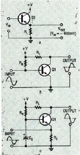
FIG. 1--THREE BASIC BIPOLAR transistor amplifier configurations.
A lot of useful information can be gained simply by studying both Fig. 1 and Table 1. The common-collector amplifier (also widely known as the emitter-follower) has its input applied between its base and collector and its output is taken across its emitter and collector.
The circuit is also referred to as the grounded collector amplifier. In practical configurations its load resistor is in series with its emitter terminal.
The mathematical derivations of the results shown in Table 1 can be found in most basic electronics texts. However, for the purposes of this article, the important characteristics of the common-collector /emitter follower amplifier to keep in mind are:
- High input impedance
- Low output impedance Voltage gain approximately equal to unity
- Current gain approximately equal to hFE
By contrast. notice that while the common-emitter and common-base amplifiers provide high voltage gain they offer only low-to medium input impedance. The applications for these circuits are governed by these characteristics.
-----------
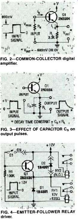
FIG. 2--COMMON-COLLECTOR digital amplifier.
FIG. 3--EFFECT OF CAPACITOR Cs on output pulses.
FIG. 4--EMITTER-FOLLOWER RELAY driver.
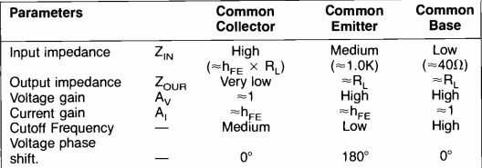
TABLE 1--CHARACTERISTICS OF THE THREE BASIC TRANSISTOR AMPLIFIERS
------------
Digital amplifiers
Figure 2 is the schematic for a simple NPN common-collector/ emitter-follower digital amplifier. The input signal for this circuit is a pulse that swings between zero volts and the positive supply voltage. When the input of this circuit is at zero volts and the transistor is fully cut off, and the amplifier's output is also zero volts-indicating zero voltage phase shift.
When an input voltage exceeding +600 millivolts (the minimum forward bias for turn-on) appears across the input terminals, the transistor turns on and current IL flows in load resistor RL, generating an output voltage across RL. Inherent negative feedback causes the output voltage to assume a value that follows the input voltage. The output voltage is equal to the input voltage minus the voltage drop across the base-emitter junction (600 millivolts). In the Fig. 2 schematic, the input (base) current is calculated as: 1H = IL/hFE Because the circuit can have a maximum voltage gain of one, it presents an input impedance calculated as: ZIN = RL X hFE Inserting the values shown in Fig. 2 yields: ZIN = 3300 ohms x 200 = 660,000 ohms The circuit has an output impedance that approximately equals the value of the input signal source impedance (Rs) divided by the hFE value of the transistor.
Because the circuit shown in Fig. 3 exhibits all of the common collector amplifier characteristics previously discussed, it behaves like a unity-gain buffer circuit. If high frequency pulses are introduced at its input, the trailing edge of the output pulse will show the time constant decay curve shown in Fig. 3. This response is caused by stray capacitance Cs (represented by dotted lines) interacting with the circuit's load resistance.
When the leading edge of the input pulse switches high, Q1 switches on and rapidly sources or feeds a charge current to stray capacitance Cs, thus producing an output pulse with a sharp leading edge. However, when the trailing edge of the input pulse goes low, Q1 switches off and effective capacitor Cs is unable to discharge or sink through the transistor.
However, Cs can discharge through load resistor RL. That discharge will follow an exponential decay curve with the time to discharge to the 37 % level equal to the product of CL and RL.
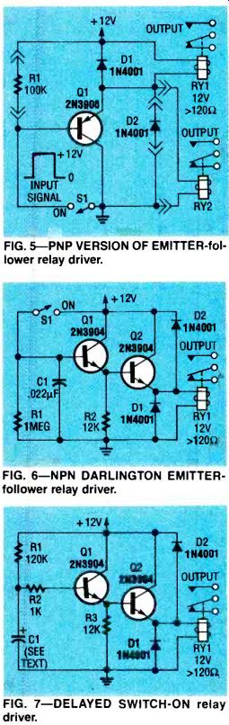
FIG. 5-PNP VERSION OF EMITTER-follower relay driver.
FIG. 6-NPN DARLINGTON EMITTER-follower relay driver.
FIG. 7--DELAYED SWITCH-ON relay driver.
Relay drivers
The basic digital or switching circuit of Fig. 2 can be put to work driving a wide variety of resistive loads such as incandescent filament lamps, LEDs or resistors. If the circuit is to drive an inductive loads such as a coil, transformer, motor, or speaker, a diode must be included to limit an input-voltage surge that could destroy the transistor when the switch is closed.
The schematic in Fig. 4 is a modification of Fig. 3 with the addition of diode D1 across the load, in this case a relay coil, and switch S1 in the collector-base circuit. It can act in either the latching or non-latching modes. The relay to be actuated either by the input pulse or switch S1.
Relay RY1's contacts close and are available for switching either when a pulse with an amplitude equal to the supply voltage is introduced or Si is closed. The relay contacts open when the input pulse falls to zero or Si is opened.
Protective diode D1 damps relay RY1's switch-off voltage surge by preventing that voltage from swinging below the zero-volt supply level. Optional diode D2 can also be included to prevent this voltage from rising above the positive power supply value. The addition of normally open relay 2 (RY2) makes the circuit self-latching.
Figure 5 shows a same relay driver circuit organized for an PNP transistor. Again, the relay can be turned on either by closing S1 or by applying the input pulse as shown.
Both the circuits shown in Figs. 4 and 5 increase the relay's sensitivity by a factor of about 200 (the hFE value of Q1). Consider a relay requires an activating current of 100 milliamperes and has a coil resistance of 120 ohms. The effective input impedance of the circuit (ZIN) will be:
ZIN = RL X hFE = 120 x 200 = 24,000 ohms
Only an input operating current of /too of 100 milliamperes or 0.5 milliamperes is required.
Circuit sensitivity can be further increased by replacing transistor Q1 with the Darlington transistor pair of Q1 and Q2, as shown in Fig. 6. This circuit presents an input impedance of about 1 megohm and requires an input operating current of about 12 microamperes.
Capacitor C1 protects the circuit from false triggering by high impedance transient voltages, such as those induced by lightning or electromagnetic interference.
The benefits of the Darlington pair are readily apparent in relay driving circuits that require time delay, such as those shown in Figs. 7 and 8. In those circuits, the voltage divider formed by resistor R1 and capacitor C1 generates a waveform that rises or falls exponentially.
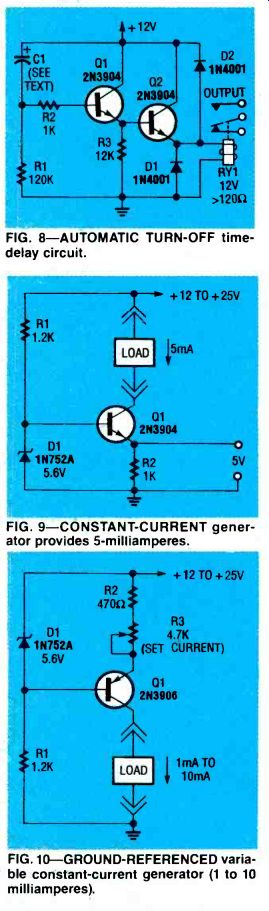
FIG. 8--AUTOMATIC TURN-OFF time-delay circuit.
FIG. 9--CONSTANT-CURRENT generator provides 5milliamperes.
FIG. 10--GROUNDREFERENCED variable constant-current generator (1 to 10 milliamperes).
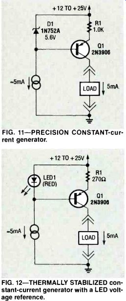
FIG. 11 PRECISION CONSTANT-current generator.
FIG. 12 THERMALLY STABILIZED constant current generator with a LED voltage reference.
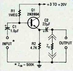
FIG. 13--SIMPLE EMITTER-FOLLOWER.
That waveform is fed to the relay coil through the high-impedance Q1-Q2 voltage following Darlington buffer. The circuit forces the relay to change state at some specified delay time after the supply voltage is applied. With the 120 K resistor R1 shown in both Figs. 7 and 8, operating delays will be about 0.1 second per micro-farad of capacitor value. For example, if C1 equals 100 micro-farads, the time delay will be 10 seconds.
In the Fig. 7 circuit, consider that C1 is fully discharged so that the R1-C1 junction is at zero volts and relay RY1 is off (contacts open) when the power supply is connected. Capacitor C1 then charges exponentially through R1, and the increasing voltage is fed to the relay circuit through Darlington pair Q1 and Q2. That causes relay RY1's contacts to close after a time delay determined by the product of R1 and C1.
Consider that capacitor C1 in the Fig. 8 circuit is also fully discharged when the power supply is connected. The junction of R1 and C1 is initially at the supply voltage, and the relay contact close at that moment.
Capacitor C1 then charges exponentially through R1, and the decaying voltage at the R1-C1 junction appears across the coil of relay RY1. The contacts of RY1 open after the delay determined by R1 and C1 times out.
Constant-current generators
A BJT can serve as a constant current generator if it is connected in the common-collector topology and the power supply and collector terminals function as a constant-current path, as shown in Fig 9. The 1000-ohm resistor R2 is the emitter load. The series combination of resistor R1 and zener diode D1 applies a fixed 5.6-volt reference to the base of Ql.
There is a 600-millivolt base-to-emitter drop across Q1, so 5 volts is developed across emitter resistor R2. As a result, a fixed current of 5 milliamperes flows through this resistor from Q1's emitter.
Because of a BJT's characteristics, emitter and collector currents are nearly identical.
This means that a 5-milliampere current also flows in any load that is connected between Q1's collector and the circuits’ positive supply. This will occur regardless of the load's resistance value-provided that the value is not so large that it drives Q1 into saturation. Therefore, these two points are constant-current source terminals.
Based on the previous discussion, it can be seen that constant current magnitude is determined by the values of the base reference voltage and emitter load resistor R2. Consequently, the value of the current can be changed by varying either of these parameters.
The Fig. 10 circuit takes this concept a step further. It can be seen, for example, that the circuit of Fig. 9 was inverted to give a ground referenced, constant current output. Adjustment of trimmer potentiometer R3 provides a current range of from 1 to about 10 milliamperes.
The most important feature of the constant-current circuit is its high dynamic output impedance typically hundreds of
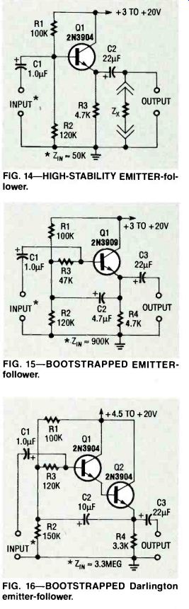
FIG. 14-HIGHSTABILITY EMITTER-follower.
FIG. 15-BOOTSTRAPPED EMITTER-follower.
FIG. 16-BOOTSTRAPPED Darlington emitter-follower.
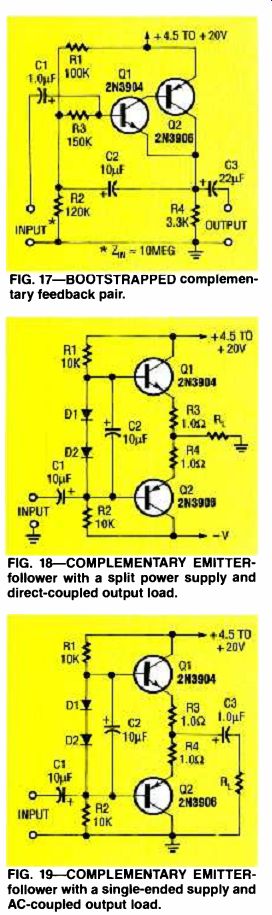
FIG. 17 BOOTSTRAPPED complementary feedback pair.
FIG. 18 COMPLEMENTARY EMITTER-follower with a split power supply and direct-coupled output load.
FIG. 19 COMPLEMENTARY EMITTER-follower with a single-ended supply and AC coupled output load.
kilohms. The precise magnitude of constant current is usually unimportant in practical circuits. The circuits shown in Figs. 10 and 11 will work satisfactorily in many practical applications.
If more precise current generation is required, the characteristics of the reference voltages of these circuits can be improved to eliminate the effects of power source variations and temperature changes.
A simple way to improve the circuits in Figs. 9 and 10 is shown in Fig. 11. Resistor R1 in both circuits can be replaced with a 5 milliampere constant-current generator. (The symbol for a constant-current generator is a pair of overlapping circles.) With a constant-current generator installed, the current through zener diode D1 and the voltage across it is independent of variations in the supply voltage.
True high precision can be obtained if the industry standard reference zener diode D1 is replaced with one having a temperature coefficient of 2 milli-volts/°C to match the base-to-emitter temperature coefficient of transistor Q1. However, if a zener diode with those characteristics cannot be located, satisfactory results can be obtained by substituting a forward biased light emitting diode, as shown in Fig 12.
The voltage drop across LED1 is about 2 volts, so only about 1.4 volts appears across emitter resistor R1. If the value of R1 is reduced from 1000 to 270 ohms, the constant-current output level can be maintained at 5 milliamperes.
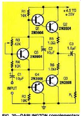
FIG. 20 DARLINGTON complementary emitter-follower with "amplified
diode" biasing from transistor Q5.
Analog amplifiers
The common collector /emitter follower amplifier can amplify AC coupled analog signals linearly if the transistor's base is biased to a quiescent value of about half the supply voltage.
This permits maximum signal swings without distortion due to clipping. As shown in Figs. 13 and 14, the analog signals are AC coupled to the base with capacitor C1, and the output signal is taken from the emitter through capacitor C2.
Figure 13 shows the simplest analog common-collector/ emitter follower circuit. Transistor Q1 is biased by resistor R1 connected between the voltage source and base. The value of resistor R1 must be equal to the input resistance RIN of the emitter follower stage to obtain half-supply biasing. Input resistance RIN (and thus the nominal R1 value) equals the 4.7 K value of R2 multiplied by the hFE value of the Q1. In this circuit: R1 = 200 x 4700 1megohm A slightly more elaborate biasing method is shown in Fig. 14.
However, its biasing level is independent of variations in transistor Q1's hFE value. Resistors R1 and R2 function as a voltage divider that applies a quiescent half supply voltage to Q1's base.
Ideally, the value of R1 should equal the value of R2 in parallel with RIN. However, the circuit works quite well if resistor R1 has a low value with respect to RIN, and resistor R2 is slightly larger than R1.
In the circuits shown in Figs. 13, and 14, the input impedance looking directly into the base of transistor Q1 equals hFE x Zload, where Z_load is equal to the combined parallel impedance of R2 and any external load Zx that is connected to the output.
In these circuits, the base impedance value is about 1 megohm when Zx is infinite. In practical circuits, the input impedance of the complete emitter follower circuit equals the combined parallel impedance of the base and bias network. The circuit shown in Fig. 13 has an input impedance of about 500 kilohms, and the circuit shown in Fig. 14 has an input impedance of about 50 kilohms.
Both the Fig. 13 and 14 circuits offer a voltage gain that is slightly less than unity; the true gain is given by:
Av = Z_load /(ZB +Z load)
Where: ZB = 251 IE ohms and IE is the emitter current in milliamperes With an operating current of 1 milliampere, these circuits provide voltage gains of 0.995 when the Z_load = 4.7 kilohms, or 0.975 when the load = 1.0 kilohm. The significance of these gain figures will be discussed shortly.
Bootstrapping
The relatively low input impedance of the circuit in Fig. 14 circuit can be increased significantly by bootstrapping as illustrated in Fig.15. The 47 kilohm resistor R3 is located between the R1-R2 biasing network junction and the base of transistor Q1, and the input signal is fed to Q1's base through capacitor C1.
Notice, however, that Q1's output signal is fed back to the R1 R2 junction through C2, so that almost identical signal voltages appear at both ends of R3. Consequently, very little signal current flows in R3. The input signal "sees" far greater impedance than the true resistance value.
To make this point clearer, consider that the emitter-follower circuit in Fig 15. has a precise voltage gain of unity. In this condition, identical signal voltages would appear at the two ends of R3, so no signal current would flow in this resistor, making it "appear" to be an infinite impedance. The input impedance of the circuit would "appear" to equal RAN, or 1 megohm.
Practical emitter-follower circuits provide a voltage gain that is slightly less than unity. The precise gain that determines the resistor amplification factor, or AR, of the circuit is: AR = 1 /(1 Ay).
For example, if circuit gain is 0.995 (as in Fig. 13), then AR is 200 and the R3 impedance is almost 10 megohms. By contrast, if MsvV = 0.975, AR is only 40 and the R3 impedance is almost 2 megohms. This impedance is effectively in parallel with RIN so, in the first example, the complete Fig. 15 circuit exhibits an input impedance of about 900 kilohms.
The input impedance of the circuit in Fig. 16 circuit can be further increased by substituting a520Darlington pair for Q1 and increasing the value of R3, as shown in Fig 16. This modification gives a measured input impedance of about 3.3 megohms.
Alternatively, even greater input impedance can be obtained with a bootstrapped complementary feedback pair" circuit as shown in Fig. 18; it offers an input impedance of about 10 megohms. In this instance, Q1 and Q2 are both connected as common-emitter amplifiers but they operate with nearly 100% negative feedback. As a result, they provide an overall voltage gain that is almost exactly one.
This transistor pair behaves like a near-perfect Darlington emitter-follower.
Emitter-followers
Recall from the previous article on bipolar transistors, Electronics Now in September 1993, a standard NPN emitter-follower can source current but cannot sink it. By contrast, an PNP emitter-follower can sink current but cannot source it.
This means that these circuits can only handle unidirectional output currents.
A bidirectional emitter-follower (that can source or sink currents with equal ease) has many applications. This response can be obtained with a complementary emitter-follower topology NPN and PNP emitter followers are effectively connected in series. Figures 18 to 20 illustrate some basic bidirectional emitter-follower circuits.
The circuit in Fig. 18 circuit has a dual or "split" power supply, and has its output is direct-coupled to a grounded load. The series-connected NPN and PNP transistors are biased at a quiescent " zero volts" value through the voltage divider formed with resistors R1 and R2 and diodes D1 and D2. Each transistor is forward biased slightly with silicon diodes D1 and D2. Those diodes have characteristics that are similar to those of the transistor base-emitter junctions.
Capacitor C2 assures that identical input signals are applied to each transistor base, and emitter resistors R3 and R4 protect the transistor against excessive output currents.
Transistor Q1 in Fig. 18 sources current into the load when the input goes positive, and transistor Q2 sinks load current when the input goes negative. Notice that input capacitor C1 is non-polarized.
Figure 19 shows an alternative to the circuit of Fig. 18 designed for operation from a single-ended power supply and an AC-coupled output load. In this circuit, input capacitor C1 is polarized.
Notice that output transistors Q1 and Q2 in Figs. 18 and 19 are slightly forward biased by silicon diodes D1 and D2 to eliminate crossover distortion problems. One diode is provided for each transistor.
If these circuits are modified by substituting Darlington pairs, four biasing diodes will be required. In those versions, a single transistor "amplifier diode" stage replaces the four diodes, as shown in Fig 20. The collector-to-emitter voltage of Q5 in Fig. 20 equals the base-to-emitter voltage drop across Q5 (600 millivolts) multiplied by (R3 +R4) /R4.
Thus, if trimmer potentiometer R3 is set to zero ohms, about 600 millivolts are developed across. Q5, which then behaves as a silicon diode. However, if R3 is set to its maximum value of 47 kilohms, about 3.6 volts is developed across Q5, which then behaves like six series-connected silicon diodes. glimmer R3 can set the voltage drop across Q5 precisely as well as adjust the quiescent current values of the Q2-Q3 stage.
------------------
Also see: TRANSISTOR COOKBOOK