An operational amplifier is just a high gain amplifier - you stick a voltage in and a much larger one comes out. But you'd never know this from the data sheets. 'Overkill' confuses all but the most experienced.. It really doesn't have to be so. Tim Orr explains ...
OP-AMPS HAVE TWO inputs, inverting and non- inverting, denoted by - and + respectively. The op-amp amplifies the difference in the voltages applied to these two inputs, the output going positive if the + input is positive with respect to the - input, and vice versa. Without extra circuitry, though, an op-amp is virtually useless, for the gain is too high to be useable and distortion is excessive. Fortunately both parameters can be controlled by feedback.
An op-amp with negative feedback is shown in Fig. 1. Two resistors set the closed loop voltage gain, and as long as this is small compared to the open loop gain, it will be determined by the resistor ratio RF/R I. The open loop gain, the voltage gain when RF is removed, is typically 1 000000. This massive gain is clearly much too large to be used without feedback.
Closed loop voltage gains of 100 are about as much as it is practical to use.
Biased example
The arrangement in Fig. 1 is known as a 'virtual earth' amplifier. The non-inverting input is connected to earth, and the inverting input is maintained by the feedback applied via RF at a voltage which is virtually earth potential.
The input impedance of the amplifier in Fig 1 is simply R1.
The output impedance is a little more complicated, approximately:- output impedance of the op amp x closed loop gain open loop gain Suppose we want an amplifier with a gain of 10, and an input impedance of 1M. This means that R1 is 1M. Therefore RF must be 10 M ( see Fig. 2). With a 1 V sinewave as the input signal we get a 10 V sinewave as the output. However, when the input signal is held at 0V, it is positive! This is an error voltage, which may be undesirable. The cause of the problem is the 'INPUT BIAS CURRENT' of the op-amp. The input of many op-amps , looks like the circuit shown in Fig. 3. If these transistors are to operate correctly they need a standing emitter current which implies that they need an input base current. It is this base current which is the op-amp's ' INPUT BIAS CURRENT'. For a 741 this current can be as large as 0.5 µA. In the arrangement of Fig. 2 this current can only come through RF, which means that the output voltage could be as large as 0.5 µA x 10 M, which is +5 V! One way to remedy this error is to use the circuit shown in Fig. 4. A resistor has been inserted between the non-inverting input and ground.
This resistor has the value of RF in parallel with R1. It allows both the inputs to sink slightly and thus maintain the voltage balance at the inputs. The output voltage is then nearly 0 V. However, the two input transistors may not be that well matched, so the bias currents into each input may be different.
This is known as the 'INPUT OFFSET CURRENT' and its effect can be nulled by making the 910 k resistor in Fig. 4 a variable resistor. But even if the bias currents ( for say a 741) were zero, then the output voltage would still not be 0V.
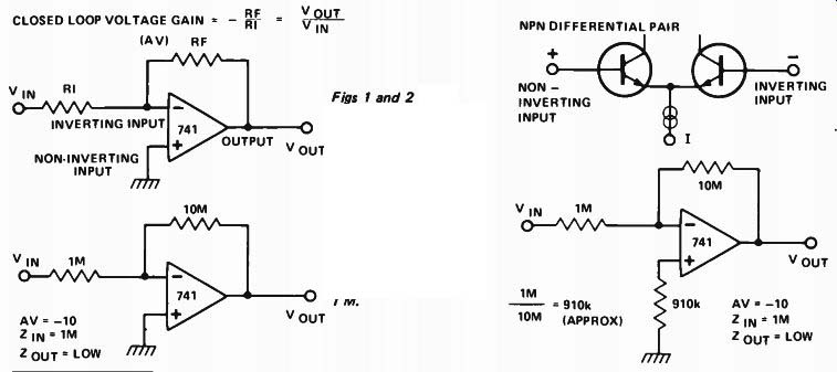
Figs 1 and 2 show (upper) the basic inverting op-amp stage. Gain is given by
the ratio of resistors RF/RI, input impedance is simply R1, while the output
impedance is more complicated (see (text).
Fig. 2 (lower) shows a stage with a gain of 10 and an input impedance of 1M.
Figs 3 and 4 (left) show (upper) a typical op-amp input stage. This is a differential amplifier made up of a pair of NPN transistors driven by a constant current source. Fig.4 (left) shows a 910 k resistor in series with the + input of the op-amp. This reduces the effects of the input offset current.
Get set, they're off
The output voltage could range between ±60 mV. This is due to the 'NPUT OFFSET VOLTAGE' which for a 741 can be as much as ±6 mV, which is then multiplied by the closed loop voltage gain of the stage ( in this case 10 giving us ±60 mV. This can be compensated by using the circuit shown in Fig. 5. Terminals 1 and 5 on a 741 can be used to compensate for the input offset voltage. The input offset voltage is the V,e imbalance between the two input transistors.
Now that we know how to eliminate the spurious dc offsets, we can try designing some dynamic circuits and find out why they don't work as expected! For example, try putting a 1 V sinewave at 200 kHz into the circuit shown in Fig. 5. What you would expect is a 10 V, 200 kHz sinewave at the output - but you don't get one. What appears is a rather bent 200 kHz triangle waveform. This is because the 'SLEW RATE' of the op-amp has been exceeded. The slew rate is the speed at which the output voltage can move, and for a 741 is typically 0.5 V/µs when it crosses zero, so the op-amp, faced with this demand, just gives up and slew limits, drawing out straight lines as it does so.
Listen to the band(width)
Another limitation is 'BANDWIDTH'. A 741 has a GAIN BANDWIDTH product of approximately 1 MHz. This means that the product of the voltage gain times the operating frequency cannot exceed 1 MHz.
For example, if you want the amplifier to have a gain of 100, then the maximum frequency at which this gain can be obtained is 10 kHz. Figure 6 illustrates this phenomenon.
Curve A is the open loop response, note that the voltage gain is 1 at 1 MHz, hence the gain bandwidth product of 1 MHz. The slope of the curve is - 20 dB/decade, which is caused by a single 30 pf capacitor inside the IC. Now, if the resistor ratio is set to give a voltage gain of 100, then the op-amp gives a frequency response shown by curve C, which is flat up until 10 kHz. A gain off 10 rolls off at 100 kHz ( D) and a gain of 1 000 rolls off at 1 kHz ( B). Thus it is very easy to see just what the closed loop frequency response will be. However, don't forget the slew rate problem. You may be able to construct an amplifier with a voltage gain of 10, which works up to 100 kHz, but the output voltage will be limited to less than 3 Vpp! Another problem is distortion in the op-amp. Negative feed back is used to iron out any distortion generated by the op amp, but negative feedback relies on there being some, spare voltage gain available. For instance, say the op-amp generates 10% distortion and there is a surplus voltage gain of 1000,
i.e. ,
open loop gain / closed loop gain,
then the distortion will be reduced to approximately,
open loop distortion / surplus voltage gain
10% / 1000 = - 0.01%
So, negative feedback is used to eliminate distortion products, However, if there is no surplus voltage gain, as in the case of a 741 amplifier working at 10 kHz, with a closed loop gain of 100, the distortion will rise dramatically at this point.
Current thinking
Most op-amps have a voltage output, although some have a current output. If you short-circuit a voltage output then large currents could flow and thermal destruction might follow. To overcome this problem, most op-amps have a current limited output so that they can tolerate an indefinite short to ground.
A 741 is limited to about 25 mA. Another current of note is the supply 'BIAS CURRENT'. This is the current consumed when the op-amp is not driving any load. For a 741 this current is typically 2 mA, which makes it unsuitable for some battery applications.
There are some op-amps which can be programmed by inserting a current into them so that their supply current can be controlled. This means that they consume only micropower when in their 'standby' mode, and can be quickly turned on to perform a particular task.
Voltages differently In the few examples shown so far, the op-amp has been used to amplify voltages which have been generated with respect to ground. However, sometimes, it is required to measure the difference between two voltages. In this case you would use a ' Differential' amplifier, Fig. 7. By using two matched pairs of resistors, the formula for the voltage gain is made very simple. It is thus possible to superimpose a 1 V sinewave on both the inputs, and yet have the output of the amplifier ignore this common mode signal and amplify only differential signals. The amount by which the common mode signal is rejected is called the CMRR (the Common Mode Rejection Ratio) and is typically 90 dB for a 741.
Thus a common mode 1 V signal would be reduced to 33 µV. Another rejection parameter to be noted is the supply voltage rejection ratio. For a 741 the typical rejection is 90 dB; that is, if the power supply changes by 1 V the change in the output voltage will be 33 µV. When designing with op-amps it is very important to know what voltage range the inputs will work over, and the maximum voltage excursion you can expect at the output. For instance, the 741 can operate with its inputs a few volts from either power supply rail, and its inputs can withstand a differential voltage of 30 V (with a power supply of 36 V). This is not true of all op-amps, some have a very limited differential input voltage range, for instance the CA3080 will zener when this voltage exceeds 5 V and the amplifier performance will then be drastically changed.
--------
Fig. 5. A variable resistor connected between pins 1 and 5 of a 741 can be
used to reduce the effects of the input offset voltage.
Fig. 6. Graph of open loop response of a 741 (A) together with curves showing response at various values of closed loop gain (B. C, 0). V1 R1
Fig. 7. Typical differential op-amp stage By using matched pairs of resistors the formula for voltage gain is made simple.
-----------
The output excursion of the op-amp is also important.
The 741 can only typically swing within about 2 V of either supply rail, whereas the CMOS op-amp can swing to within 10mV of either rail so long as the load into which they are driving is a very high impedance.
12 V REGULATED POWER SUPPLY
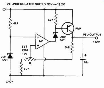
--------- The large open loop voltage gain of an op-amp is very useful in
providing a regulated low output impedance power supply.
A 5V1 voltage reference is generated by a zener diode ZD1 (this voltage reference could be made more stable by running it at constant current). A PNP transistor is used as a series regulator. However, this transistor inverts the signal from the op-amp output, and so, in order to get negative feedback, the feedback is taken to the non-inverting input! The operations is as follows. The inverting input is held at 5V1. If the ' PSU OUTPUT' tries to fall, the voltage at the non-inverting input falls. Therefore the op-amp's output will also fall, thus turning on the PNP transistor which then pulls up the ' PSU OUTPUT'. Thus the output voltage is stabilized. Also, the output impedance is very low, due to this negative feedback. The output impedance at high frequencies (where the op-amp gain is low) is further reduced by the 10 µ capacitor. To squeeze the last drop of voltage out of the system, before a collapsing unregulated supply rail causes the regulated supply to drop out, a 5V1 zener diode ( ZD2) has been included. This allows the op-amp output to work at about 7 volts below the unregulated supply rail. Thus, a regulated output is maintained until the PNP transistor saturates. This means that the unregulated rail can fall to within about 200 mV of the regulated rail!
SIMPLE INTEGRATOR
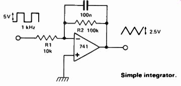
---------- Simple integrator.
An op-amp and a capacitor can be used to implement, to a high degree of accuracy, the mathematical process of integration. In this case, current is summed over a period of time and the resultant voltage generated is the integral of that current as a function of time. What this means that if a constant voltage is inputted to the circuit, a ramp with a constant slope is generated at the output. When the input is positive, the output of the op-amp ramps negative.
In doing so it pulls the inverting terminal negative so as to maintain a 'virtual earth' condition. In fact the input current (Vin/R1) is being equaled by the current flowing through the capacitor, thus equilibrium is maintained. The equation governing the behavior of a capacitor is
C x dV/dt = where dV/dt is the rate of change of voltage across the capacitor.
Therefore Thus dV ± dV Vin dt C dt R1C So, when a square wave is applied to the circuit in Fig. 10, triangle waveforms are generated. R2 was added to provide DC stability. Its inclusion does slightly corrupt the mathematical processes, but not enormously. A good point about this integrator design is that it has a very low output impedance. You can put a load on the output and the op-amp will still generate the same waveform - that's what is so nice about negative feedback.
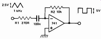
Fig. 11. Simple differentiator.
SIMPLE DIFFERENTIATOR
Mathematically, differentiation is the reverse process to integration. Thus, in the differentiator circuit the C and the R are reversed with respect to the integrator circuit.
The input waveform is a triangle with a constant rise and fall slope. This constant slope, when presented to a capacitor will generate a constant current. When the slope direction reverses, then so will the current flow. This current when passed through a resistor ( R1), will then generate a square wave.
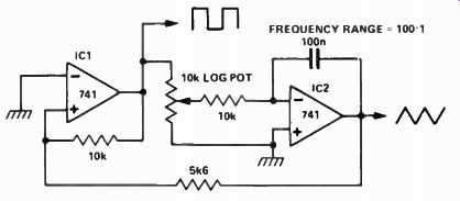
TRIANGLE SQUARE OSCILLATOR
A Schmitt trigger and an integrator can be used to construct a very reliable oscillator which generates triangle and square waveforms. The operation of the circuit is very simple and always self starting. The Schmitt trigger is formed from IC1, the integrator from IC2. Suppose the output of the Schmitt is positive. This will cause the integrator to generate a negative going ramp. This ramp is then fed back to the input of the Schmitt. When the lower hysteresis level has been reached the output of the Schmitt snaps into its negative state, current is taken out of the integrator which then generates a positive going ramp. The integrator's output ramps up and down between the upper an lower hysteresis levels. The speed at which the integrator moves is determined by the magnitude of the voltage applied to it. In this circuit, the magnitude of the voltage and hence the oscillation frequency, are controlled by a potentiometer, giving a 100 to 1 control range. This
-------------
-------
circuit is the basis of most function generators. By bending the triangle it is possible to synthesize an approximation to a sinewave. With a bit more electronics it is also possible to make the oscillator voltage controlled.
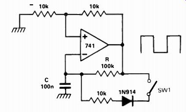
SINGLE OP-AMP OSCILLATOR
-------------
This circuit has a Schmitt trigger and a ' sort of integrator' all built around one op-amp. The positive feedback is via the 10 k resistors. The ' integration', ( the timing) is controlled by the RC network. The voltage at the inverting input follows that of the RC charging exponential, except that it is confined to be within the upper and lower hysteresis levels.
Thus the hysteresis levels and the RC time constant determine the frequency of operation. It is possible to make the output square wave have a large mark to space ratio. By closing the switch SW1, the discharge time of the capacitor becomes eleven times faster than the rise time. Thus a square wave with an 11:1 mark space ratio is generated.
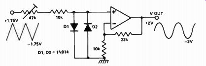
SIMPLE TRIANGLE TO SINEWAVE CONVERTER
Here is a simple way of converting a triangle to a sinewave.
The logarithmic characteristic of the diodes is used to approximate that of a sine curve. Distortion is 5% or so. However, the distortion may be tolerable if the sinewave is only used to generate audio tones.
LINEAR VOLTAGE CONTROLLED OSCILLATOR
This oscillator is very similar to the triangle square wave oscillator shown on this page, except that this one is voltage controlled. The integrator and Schmitt trigger action are the same as before, but the feedback has been altered. The input voltage Vin, is applied differentially to the integrator via the resistor network. The larger the value of Vin, the faster the integrator ramps up and down. Thus the frequency of the operation is determined by an external positive control voltage.
The frequency is linearly proportioned to this control voltage.
When the output of the Schmitt is low, Q1 is off and all the input voltage is applied to the inverting input. Half of the input voltage is always applied to the non-inverting input.
Therefore the integrator's output ramps downward until the Schmitt flips into its positive state. Now, Q1 is switched on and the voltage at the inverting input is negative with respect to the non-inverting input. Hence the integrator now ramps upwards.
------
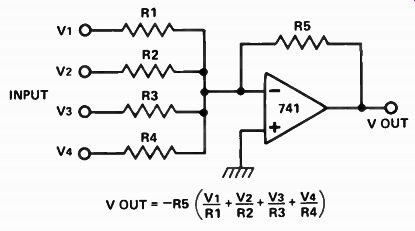
BASIC SUMMING CIRCUIT (MIXER)
A virtual earth amplifier can be used to mix several signals together. The output voltage is a mixture of all the inputs.
The amount of an input that appears at the output is inversely proportional to the input resistor. If the input voltages are fed into potentiometers before being fed to the mixer, then their individual levels can be manually adjusted. This is the basis of most audio mixers, although the cheaper units use op amps. Most op-amp mixers will degrade the signal to noise ratio of the signals by more than a good discrete component amplifier.
-------
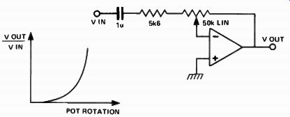
TURNING A LINEAR POT INTO A LOG POT
By using the virtual earth characteristic of an op amp, a linear pot can be made to have the characteristics of a log pot. It seems to be fair to say that low cost linear pots are far more linear than log pots are logarithmic. Thus the linear pot can be turned into a better log pot than the actual log pot itself. By varying the resistor ratio 5k6 to 50 k, other laws can be produced, such as something in between log and linear or maybe a law that is even more extreme than log.
-----------
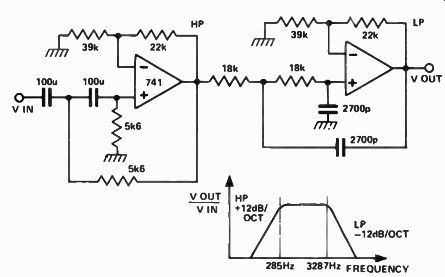
SIMPLE SPEECH FILTER
The telephone system has been designed for speech communication. The bandwidth of the system is
-10(LtiLieLl)11 1.z,
which has been arrived at after many years of experimentation. Thus, it is true to say that much of the information in speech is contained between these frequency limits.
The circuit shows a filter structure that will simulate the telephone bandwidth. It could have many uses, for instance as a 'speech filter' for noisy radio reception or land line communications, or as a voice detector for a light show.
--------------
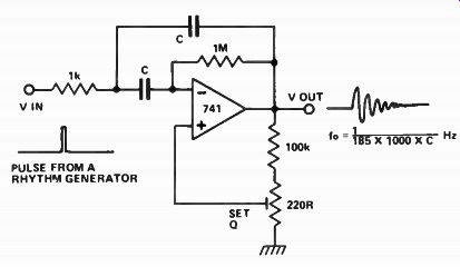
SIMPLE MUSICAL CHIME GENERATOR
The circuit shown is that of a multiple feedback band-pass filter. The presee is used to add some positive feedback and so further increase the Q factor. The principle of operation is as follows. A short click ( pulse) is applied to the filter and this makes it ring with a frequency which is its natural resonance frequency. The oscillations die away exponentially with respect to time and in doing so closely resemble many naturally occurring percussive or plucked sounds. The higher the CI the longer the decay time constant. High frequency resonances resemble chimes, whereas lower frequencies sound like claves or bongos, By arranging several of these circuits, all with different tuning, to be driven by pulses from a rhythm generator an interesting pattern of sounds can be produced. There may be some stability problems when high Q or high frequency operation is involved. To achieve better performance, an op amp with a greater bandwidth than the 741 should be used.
Alternatively, a different structure, such as a state variable filter could be used. Qs of up to 500 can be obtained with this latter circuit.
------------
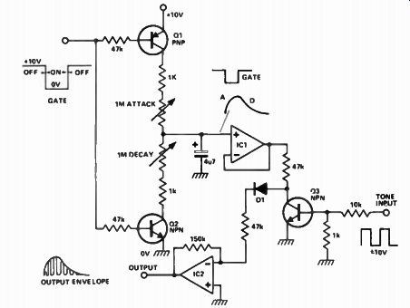
MUSICAL ENVELOPE GENERATOR AND MODULATOR
A gate voltage is applied to initiate the proceedings. When the gate voltage is in the ON state, Q1 is turned on, and so the capacitor C is charged up via the attack pot in series with the 1 k resistor. By varying this pot, the attack time constant can be manipulated. A fast attack gives a percussive sound, a slow attack the effect of 'backward' sounds. When the gate voltage returns to its off state, Q2 is turned on and the capacitor is then discharged via the decay pot and the other 1 k resistor, to ground. Thus the decay time constant of the envelope is also variable.
This envelope is buffered by IC1, a high impedance voltage follower and applied to Q3 which is being used as a transistor chopper. A musical tone in the form of a squarewave is connected to the base of Q3. This turns the transistor on or off and thus the envelope is chopped up at regular intervals, the intervals being determined by the pitch of the squarewave.
The resultant waveform has the amplitude of the envelope and the harmonic structure of the squarewave. IC2 is used as a virtual earth amplifier to buffer the signal and DI ensures that the envelope dies away at the end of a note.
--------------
SIMPLE MUSICAL ENVELOPE GENERATOR
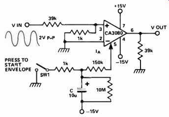
---------- A simple generator can be constructed using the CA3080 (made
by RCA). This circuit will also enable the use of an audio waveform the harmonic
structure of which will not be VIN 6 V OUT significantly affected as it is
modulated. The CA3080 is an 2V PP op amp with a difference. It has a current
output and an extra input into which a current, I A is fed. The output is the
A 39k product of the input voltage X I A . Thus the I A can be used to control
the amplifier's gain. The input voltage range for low distortion operation
is very low, of the order of ± 25 mV. The CA3080 is being used as a two-quadrant
multiplier. A small voltage, (± 25 mV), is applied to its non-inverting input.
When the switch S1 is closed, the Capacitor C is charged up and a current of about 150 pA flows into the' IA input terminal. When Si is opened, C discharges through the 150 k resistor into the I A input. This current dies away exponentially. an exponential envelope is generated. Breakthrough after the As the output is the product of the input voltage X I A , then decay is very good, better than -80 dB.
SILENT AUDIO SWITCHING
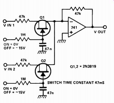
----------- Sometimes electronic switches for audio signals are required.
FETs can be used to perform the switching, but they can cause distortion, the resultant output impedance is not very low and clicks generated by the switching signal can break through. The circuit shown virtually eliminates all of these problems. By using an op-amp a very low output impedance is obtained as well as the possibility of selecting or mixing one or more of many input channels. Because of the virtual earth mixing, the voltage across any FET that is switched on is very small. If the output voltage is 1V and the FETs ON resistance is 470R, then the voltage across the FET is about 10 mV. When large voltages are applied to a turned on FET, the distortion is large, but if the voltage is small, ( 10 mV say), the distortion could be less than 0.1%. Thus the virtual earth mixing enables low distortion operation. Lastly, to stop the generation of switching clicks, a time constant of 47 msec has been enforced at the gate of the FETs.
LED BAR PPM DISPLAY FOR AUDIO
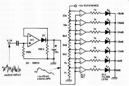
---------
The peak voltage detector can be used to control an illuminated audio level monitor having the same characteristics as a PPM (Peak Program Meter). A bar column of LEDs is arranged so that as the audio signal level increases, more LEDs in the column light up. The LEDs are arranged vertically in 6 dB steps. A fast response time and a one second decay time has been chosen so as to give an accurate response to transients and a low 'flicker' decay characteristic. The op-amps that drive the LEDs are used as comparators. On each of their inverting inputs they have a dc reference voltage, which increases in 6 dB steps up the chain. All of their non-inverting inputs are tied together and connected to the positive peak envelope of the audio signal. Thus as this envelope exceeds a particular voltage reference, that op-amp output goes high and the LED lights up. Also, all the LEDs below this are illuminated.
ALL-PASS NOTCH FILTER
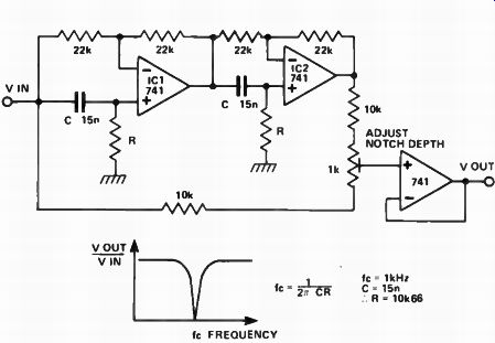
---------- Sometimes when processing analog signals a constant tone causes
a nuisance and so an active filter is called upon to 'notch' it out. The filter
can be tuned so that its notch is at exactly the same frequency as the unwanted
signal so that it can be selectively attenuated. This method is sometimes used
to remove mains hum. The circuit works as follows IC1 and 2 are a pair of all-
pass filters. These filters have a flat frequency response, but their phase
changes with frequency. Their overall maximum phase shift is 360°, a phase
shift of 180° occurring at a frequency of 1/2CR Hz. At this frequency the signals
are inverted. Thus, by mixing the phase delayed signal with the original, cancellation
can be produced which forms a notch in the frequency response. The preset is
used to get the deepest notch available. The operating frequency can be changed
by varying the two resistors R. For instance for 50 Hz operation, R should
be: 10.66k X 1000 = 213.2 k
Nearest E12 fit is 220 k 50
NOISE GENERATOR
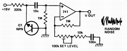
-----------
The zener breakdown of a transistor junction is used in many circuits as a noise generator. The breakdown mechanism is random and so generates a small noise voltage. Also this voltage has a high source impedance. By using the op-amp as a high input impedance, high ac gain amplifier, a low impedance, large signal noise source is obtained. The preset is used to set the noise level by varying the gain from 40 to 20 dB.
LOGARITHMIC VOLTAGE TO VOLTAGE CONVERTER
--------- The output voltage is logarithmically proportional to the input
voltage. The difference between this circuit and the previous is that the exponentiator
is in the feedback loop of the op-amp and hence the mathematical function has
been inverted. The circuit is useful for performing true logarithmic compression
or for converting linear inputs into dBs.
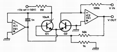
EXPONENTIAL VOLTAGE TO CURRENT/VOLTAGE CONVERTER
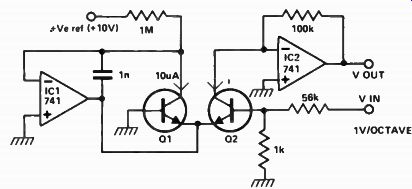
------ The circuit shown converts a linear input voltage into
an exponential current or voltage. This type of circuit is used in music synthesizers
to change linear control voltages into musical intervals. That is, if the circuit
were used to control an oscillator, input increments of 1 V would change the
pitch by one octave. The exponential characteristics of a transistor are ex-ployed
to generate the correct transfer function. Q1 and Q2 are matched pairs of transistors,
preferably a transistor dual.
IC1 maintains Q1 at a constant current. Thus, the op-amp serves only to bias the emitter of the second transistor Q2 into a suitable operating region. The purpose of Q1 is to generate this bias voltage. The base emitter junction of a transistor has a high temperature coefficient (- 1.9 mV/°C) and so the reason for using a matched pair is to use the first transistor, Q1, to provide temperature compensation for the second.
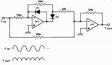
PRECISION HALF WAVE RECTIFIER
------
Rectifying small signals with any accuracy can be very difficult using diodes only due to their forward voltage drop of about 0.6 V. However, an op-amp can be used to reduce this voltage drop to virtually nothing. Consider the circuit shown. There is negative feedback so that 'virtual earth' circumstances exist.
When Vin is positive, D1 conducts to maintain the virtual earth, D2 is reverse biased and so the output is just a 100 k resistor connected to 0 V. When Vin goes negative, the output rises positively, D2 is turned on and D1 turned off. As the virtual earth is being maintained, the output voltage is the exact inverse of the input voltage. This is true for all negative inputs. Therefore, the output is composed of positive going half sinewaves. Precision half wave rectification has occurred.
In fact the diode error is very small, being equal to 600 mV (surplus voltage gain.
Therefore as the input frequency increases, and the surplus voltage gain decreases, precision falls.
By adding together the original and the half wave rectified signals together in the right ratio, it is possible to fill in the half cycle gaps and thus to generate precise full wave rectification. The addition of one summing op-amp and three resistors is all that is needed as shown opposite.
VOLTAGE TO CURRENT CONVERTER
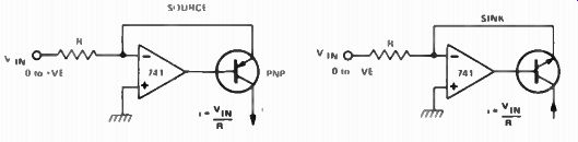
------ The virtual earth of an op-amp and the current source characteristic
of a transistor can be combined to produce a precision linear voltage to current
converter. Consider the 'SOURCE' circuit. A positive voltage is applied and
the op-amp adjusts itself so that a 'virtual earth' condition is maintained.
This means that a current i flows through the input resistor R, where i = Vin/R.
Now this current has to go somewhere, and so it flows through the PNP transistor
and comes out of the collector and into its load. Thus, the input voltage generates
a current which is linearly proportional to it.
There are, however, three sources of error that will affect this linearity. First the input offset voltage of the op-amp may become significant at low levels of Vin. Second, the input bias current may well rob a lot of the current when Vin is low.
Third, the base current of the transistor must be subtracted from the final output current. Note that the current gain of the transistor will change with collector current variations, and so the base current loss is not a fixed percentage. However, a precise voltage to current converter can be made using an op-amp with a F ET input so that the bias current is low. Also, an input balance can be used to zero out the input offset voltage, and if a FET is used to replace the bipolar transistor, then the base current problem can be removed.
The 'SINK' circuit merely swaps the transistor to an npn type. Note that the input voltage now must be negative.
NON- INVERTING AMPLIFIER:
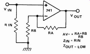
-------- An op-amp is used to provide voltage gain, but in this case
the output is in phase with the input. The minimum voltage is unity and occurs
when RB is an open circuit. The op-amp has maximum bandwidth at unity gain,
and any increase in the gain will cause a reciprocal decrease in bandwidth.
HIGH SLEW RATE AMPLIFIER
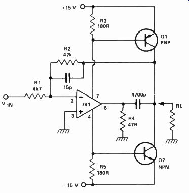
--------
The slew rate of the op-amp has been increased by increasing the overall current generating capability, by the addition of a pair of transistors. These transistors increase the output voltage range by allowing the voltage to swing to within OV5 of either supply rails. The output of the op-amp hardly moves at all. Without an input signal, the output voltage is 0 V and the op-amp drains approximately 2 mA from the supply rails.
This current passes through the 180R resistors and sets up a voltage which is not quite sufficient to turn on either transistor. When a positive voltage is applied to the input, the op-amp tries to swing negative but it has a 47R ( R4) resistor connected from its output to ground. Thus, as it tries to swing negative, it draws lots of current from the negative rail. This current flows through R5, and in doing so turns on Q2. This transistor then pulls R2 down and thus provides negative feed back. The same sequence of events occurs when the input is negative except that R3 and Q1 are then involved. Thus the high current capabilities of discrete transistors are combined with a high voltage gain of an op-amp to produce a moderately powerful amplifier. The voltage gain is set by R2/R1.
Transistors Q1 and Q2 introduce a phase shift, which may give rise to a high frequency instability and oscillation. This can be cured by some frequency compensation applied to the amplifier or by increasing the overall voltage gain.
SCHMITT TRIGGER
When dc positive feedback is applied around an op-amp, its output will come to rest in one of two states, that is in its most positive or most negative position. This type of circuit is known as a Schmitt Trigger and it is said to exhibit the property of hysteresis.
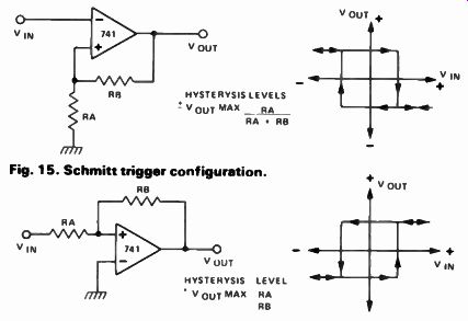
Fig. 15. Schmitt trigger configuration.
Consider the circuit shown in Figure 15. Let us assume that RB is 2 k and RA is 1 k and the output voltage is + 10 V. Therefore the voltage at the non- inverting terminal is 3V3.
When the input voltage becomes more positive than 3V3, the output of the op-amp will start to swing negative and in doing so will increase the voltage difference between the inputs. This will in turn make the output swing even more negative. Thus the process becomes regenerative, the output finally 'snapping' into its negative state (- 10 V say). The only thing that will now change the op-amp's output is if the inverting input goes more negative than the non-inverting input. When this occurs it will revert back to its original state. The two input voltages at which these transitions happen are known as the upper and lower hysteresis levels.
HIGH PERFORMANCE SAMPLE AND HOLD
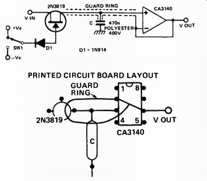
------- It is often necessary to have a circuit that will sample an
analog voltage and then remember it for a long time without any significant
degradation of that voltage. This is known as a sample and hold circuit and
one of its uses is to store the voltage from the keyboard connected to an electronic
music synthesizer.
The ,voltage is then used to control the pitch of a voltage controlled oscillator and so it is very important to have a high performance sample and hold. A drift of less than one semi tone, (80 mV), in ten minutes is required. A sample and hold is simply an electronic switch, a storage capacitor and a high input impedance voltage follower. In the circuit shown, when switch SW1 is positive the FET is turned on, and has a resistance of about 400R. Thus the input voltage charges up the capacitor through the FET. When SW1 is negative, the FET is turned off, ( pinched off), and can have a resistance of thousands of megohms. To get a long storage time the op-amp must have a very low input bias current. For the CA3140, this current is about 10 pico amps, i.e., 10-11 amps. Therefore the rate at which the capacitor will be discharged by this current can be worked out from the equation, C(dv/dt) = where dv/dt is the rate of change of voltage on the capacitor.
Therefore: dv = i = 10-11 22 uV/s dt C 0.47 X 10^-6
This is a very low drift rate, much better than we need. however, the actual drift rate will probably be in excess of this, due to surface leakage on the printed circuit board, leakage through the FET, and internal leakage in the capacitor. It is advisable to use a high voltage, non-polarised capacitor in this circuit to keep the leakage currents to a minimum. Also, to stop surface leakage a simple PCB trick can be used, that of making a guard ring around the sensitive components.
Normally any potential stored on the capacitor may leak to ground across the surface of the PCB, but if we make the surrounding surface a conducting track held at the same potential as that of the capacitor then the potential difference is virtually always zero, and hence the surface leakage is greatly reduced.
CLEANING UP DIGITALLY GENERATED SIGNALS WITH TWO SAMPLE AND HOLDS AND AN INTEGRATOR
The output from a digital to analog converter (dac) is composed of a series of steps which have been selected by a series of binary numbers. The output of the dac may represent the result of some computation done by a microprocessor or the contents of a digital memory. If the number of bits that control the dac is low ( less than eight), then the output will look like a series of discrete steps, plus lots of digital 'glitches'. Therefore, if this signal is to be displayed on an oscilloscope, the overall picture quality will be very poor. One way to clean up would be to join up all the steps with straight lines and if done successfully a great improvement can be obtained. The only problem is that the distance between steps is continuously varying and so the slope of the straight lines will need to be variable as well. This process is known as linear point interpolation and can be achieved with two sample and holds and an integrator.
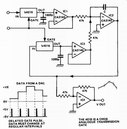
--------
A delayed gate pulse is generated, so that once the dac's output has settled, the sample and hold switches momentarily open, sample the information and then close. The output of the first sample and hold ( IC1) drives an integrator ( IC2), the output of which drives the second sample and hold ( IC3). The second unit provides negative feedback around the integrator, but it is delayed by one time interval. Thus a momentary positive going signal will pass through the first sample and hold and cause the integrator to ramp in a negative direction. When the next time interval arrives, the first sample and hold returns to OV, and the second obtains a negative voltage. This then causes the integrator to ramp positively. The size of the integrator's capacitor C should be chosen to suit the clock speed of the dac. An inverter, IC4 has been included to correct the invertion caused by the integrator.
FAST SYMMETRICAL ZENER CLAMPING
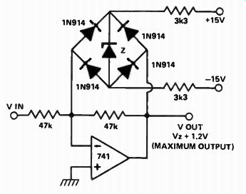
------ There are several problems with using zeners, back to back
in series to get symmetrical clamping, the knee of the zener characteristics
is rather sloppy, charge storage in the zeners causes speed problems and the
zeners will have slightly different knee voltages so the symmetry will not
be all that good. This circuit overcomes these problems. By putting the zener
inside a diode bridge the same zener voltage is always experienced. The voltage
errors due to the diodes are much smaller than those due to the zener. Also
the charge storage of the bridge is much less. Lastly by biasing the zener
on all the time, the knee appears to be much sharper.
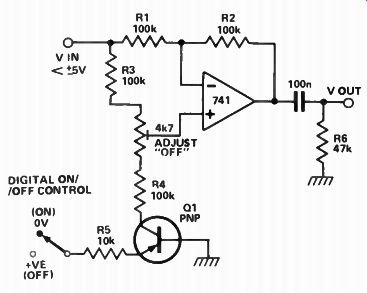
TRANSISTOR USED TO TURN AN OP AMP ON OR OFF
-----
When transistor Q1 is switched off, the circuit behaves as a voltage follower. By applying a positive voltage to the emitter of C11 via a 10 k resistor, the transistor is made to turn on and go into saturation. Thus the lower end of R4 is shorted to ground. The circuit has now changed into that of a differential amplifier ( see fig. 7), but where the voltage difference is always 0 V. Now as long as the resistors in the two branches around the op amp are in the same ratio then there should be zero output. A 4k7 preset is used to null out any ratio errors so that the 'OFF' attenuation is more than 60 dB. The high common mode rejection ratio of a 741 enables this large attenuation to be obtained.
No Noise is Good Noise
The last op-amp characteristic to be discussed is 'Noise'. The noise figures given in the specifications are very confusing.
This is due to the fact that noise is specified in so many different ways that it is often difficult to compare devices.
One may be specified in terms of Equivalent Input Noise and another device in terms of ohm IA/ Hz ( nano volts per root Hertz)! As a generalization it is true to say that most op amps are relatively noisy. Some op-amps are labeled low noise, and these are quieter than the average op-amp but more noisy than a well designed discrete component amplifier. For audio work you can use ordinary op-amps for processing high level signals ( 100 mV to 3 V), but for amplifying low level signals ( 1 mV to 100 mV) you would be advised to use a low noise device. The larger the voltage gain you obtain from an op-amp stage, the worse will be the noise, therefore keep the closed loop gain to a bare minimum.
That is the end of the theory, now for some practical examples of op-amps in use.
For more great circuit ideas...
----------
FROM THE PUBLISHERS OF ELECTRONICS TODAY INTERNATIONAL-- now at all main news agents $2.95 or direct from ETI at $3.40 inc p & p.

---- Project construction and debugging is so much easier if you have the
appropriate test equipment. The same applies when servicing manufactured electronic
equipment. Our first Test Gear book was extraordinarily popular. Test Gear
2, assembles 27 of our test instrument projects published over the last few
years in one handy volume, including: 487 Audio Spectrum Analyzer, 320 Battery
Condition Indicator, 717 Crosshatch Generator, 135 Digital Panel Meter, 132
Experimenter's Power Supply, 719 Field Strength/ Power Meter, 140 1GHz Frequency
Meter, 141 Logic Trigger, 129 RF Signal Generator, 139 SWR/Power Meter, 222
Transistor Tester, 148 Versatile Logic Probe - and more. Price: $3.95 plus
55 cents postage and handling, from ETI, Subscription Department, 15 Boundary
St, Rushcutters Bay NSW 2011. Also available from newsagents and selected electronics
suppliers.