OPERATIONAL AMPLIFIERS (OP-AMPS) CAN be simply described as high-gain direct-coupled voltage amplifier ' blocks' that have a single output terminal but have both inverting and non- inverting input terminals.
Op-amps can readily be used as inverting, non- inverting, and differential amplifiers in both a.c. and d.c. applications, and can easily be made to act as oscillators, tone filters, and level switches, etc.
Op-amps are readily available in integrated circuit form, and as such act as one of the most versatile building blocks available in electronics today. One of the most popular op-amps presently available is the device that is universally known as the "741" op-amp In this article we shall describe the basic features of this device, and show a wide variety of practical circuits in which it can be used.
BASIC OP-AMP CHARACTERISTICS AND CIRCUITS
In its simplest form, an op-amp consists of a differential amplifier followed by offset compensation and output stages, as shown in Fig. 1a. The differential amplifier has inverting and non- inverting input terminals, a high-impedance (constant current) tail to give a high input impedance and a high degree of common mode signal rejection. It also has a high- impedance (constant current) load to give a high degree of signal voltage stage gain.
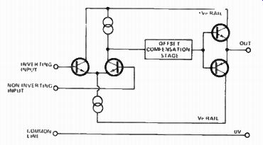
Fig. 1a Simplified op- amp equivalent circuit.
The output of the differential amplifier is fed to a direct-coupled offset compensation stage, which effectively reduces the output offset voltage of the differential amplifier to zero volts under quiescent conditions, and the output of the compensation stage is fed to a simple complementary emitter follower output stage which gives a low output impedance.
INVERTING INPUT OUT NON-INVERTING INPUT
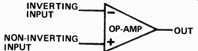
Fig. 1b Basic op-amp symbol.
LINES OF SUPPLY
Op-amps are normally powered from split power supplies, providing + ve, - ve, and common (zero volt) supply rails, so that the output of the op-amp can swing either side of the zero volts value, and can be set at a true zero volts ( when zero differential voltage is applied to the circuits input terminals.)
The input terminals can be used independently (with the unused terminal grounded) or simultaneously, enabling the device to function as an inverting, non- inverting, or differential amplifier. Since the device is direct-coupled throughout, it can be used to amplify both a.c. and d.c. input signals. Typically, they give basic low-frequency voltage gains of about 100 000 between input and output, and have input impedances of 1M or greater at each input terminal.
Fig. 1b shows the symbol that is commonly used to represent an op-amp, and 1c shows the basic supply connections that are used with the device. Note that both input and output signals of the op-amp are referenced to the ground or zero volt line.
SIGNAL BOX
Fig. 1c Basic supply connections of an op-amp.
The output signal voltage of the op-amp is proportional to the DIFFERENTIAL signal between its two input terminals, and is given by
--Ao(e,-e 2)
where A.- the open- loop voltage gain of the op-amp (typically 100 000).
e1 = signal voltage at the non- inverting input terminal.
e2= signal voltage at the inverting input terminal.
Thus, if identical signals are simultaneously applied to both input terminals, the circuit will ( ideally) give zero signal output If a signal is applied to the inverting terminal only, the circuit gives an amplified and inverted output.
If a signal is applied to the non-inverting terminal only, the circuit gives an amplified but non-inverted output.
By using external negative feedback components, the stage gain of the op-amp circuit can be very precisely controlled.
REFERENCE VOLTAGE (e2) SAMPLE VOLTAGE (et )
SUPPLY Ve SUPPLY
-Ve OUTPUT
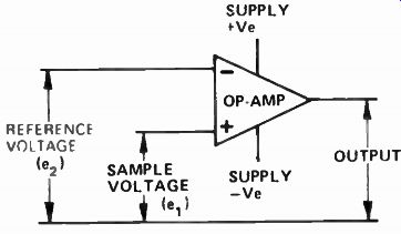
Fig. 2a
Simple differential voltage comparator circuit.
TRANSFER REQUEST
Fig. 2a shows a very simple application of the op-amp. This particular circuit is known as a differential voltage comparator, and has a fixed reference voltage applied to the inverting input terminal, and a variable test or sample voltage applied to the non-inverting terminal. When the sample voltage is more than a few hundred microvolts above the reference voltage the op-amp output is driven to saturation in a positive direction, and when the sample is more than a few hundred microvolts below the reference voltage the output is driven to saturation in the negative direction.
Fig. 2b shows the voltage transfer characteristics of the above circuit. Note that it is the magnitude of the differential input voltage that dictates the magnitude of the output voltage, and that the absolute values of input voltage are of little importance. Thus, if a 1V reference is used and a differential voltage of only 200uV is needed to switch the output from a negative to a positive saturation level, this change can be caused by a shift of only 0.02% on a 1V signal applied to the sample input. The circuit thus functions as a precision voltage comparator or balance detector.
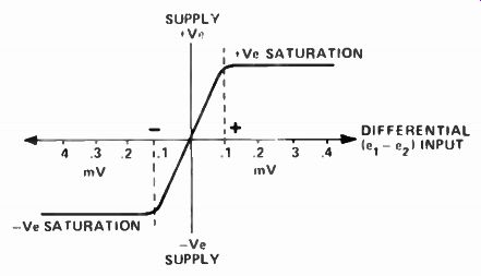
Fig. 2b Transfer characteristics of the differential voltage comparator circuit.
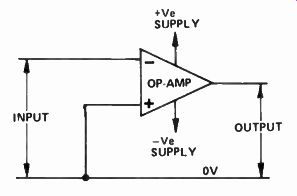
Fig. 3a Simple open-loop inverting d.c. amplifier.
-Ve
SUPPLY 0V OUTPUT
The op-amp can be made to function as a low-level inverting d.c. amplifier by simply grounding the non- inverting terminal and feeding the input signal to the inverting terminal, as shown in Fig. 3a. The op-amp is used ' open-loop (without feedback) in this configuration, and thus gives a voltage gain of about 100 000 and has an input impedance of about 1M. The disadvantage of this circuit is that its parameters are dictated by the actual op-amp, and are subject to considerable variation between individual devices.
CLOSING LOOPS
A far more useful way of employing the op-amp is to use it in the closed-loop mode, i.e., with negative feedback. Fig. 3b shows the method of applying negative feedback to make a fixed- gain inverting d.c. amplifier. Here, the parameters of the circuit are controlled by feedback resistors R, and R,. The gain, A of the circuit is dictated by the ratios of A, and R,. and equals 1:1 2/ R
The gain is virtually independent of the op-amp characteristics, provided that the open-loop gain (A„) is large relative to the closed-loop gain (A). The input impedance of the circuit is equal to R,, and again is virtually independent of the op-amp characteristics.
741 COOKBOOK
It should be noted at this point that although R1 and R2 control the gain of the complete circuit, they have no effect on the parameters of the actual op-amp, and the full open- loop gain of the op-amp is still available between its inverting input terminal and the output.
Similarly, the inverting terminal continues to have a very high input impedance, and negligible signal current flows into the inverting terminal. Consequently, virtually all of the R, signal current also flows in R,, and Fig. 4a Basic non inverting d.c. amplifier signal currents i, and i, can be regarded as being equal, as indicated in the diagram.
Since the signal voltage appearing at the output terminal end of R, is A times greater than that appearing at the inverting terminal end, the current flowing in R2 is A times greater than that caused by the inverting terminal signal only. Consequently, R, has an apparent value of R2/A when looked at from its inverting terminal end, and the R,- R, junction thus appears as a low- impedance VIRTUAL GROUND point.
INPUT VIRTUAL GROUND POINT
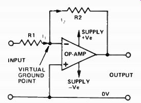
Fig. 3b Basic closed-loop inverting d.c. amplifier.
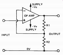
INVERT OR NOT TO INVERT ... It can be seen from the above description that the Fig. 3b circuit is very versatile. Its gain and input impedance can be very precisely controlled by suitable choice of R, and R,, and are unaffected by variations in the op-amp characteristics. A similar thing is true of the non- inverting d.c. amplifier circuit shown in Fig. 4a. In this case the voltage gain is equal to ( R,-f- R2)/ R, and the input impedance is approximately equal to (Ao/A)Zin where Zin is the open- loon input impedance of the op-amp. A great advantage of this circuit is that it has a very high input impedance.
FOLLOW THAT VOLTAGE
The op-amp can be made to function as a precision voltage follower by connecting it as a unity-gain non- inverting d.c. amplifier, as shown in Fig. 4b. In this case the input and output voltages of the circuit are identical, but the input impedance is very - high and is roughly equal to A,, X Z,„.
The basic op-amp circuits of Figs. 2a to 4b are shown as d.c. amplifiers, but can readily be adapted for a.c. use. Op-amps also have many applications other than as simple amplifiers. They can easily be made to function as precision phase splitters, as adders or subtractors, as active filters or selective amplifiers, as precision half- wave or full- wave rectifiers, and as oscillators or multivibrators, etc.
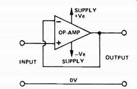
Fig. 4b Basic unity-gain d.c. voltage follower
OP-AMP PARAMETERS
An ideal op-amp would have an infinite input impedance, zero output impedance, infinite gain and infinite bandwidth, and would give perfect tracking between input and output. Practical op-amps fall far short of this ideal, and have finite gain, bandwidth, etc., and give tracking errors between the input and output signals. Consequently, various performance parameters are detailed on op-amp data sheets, and indicate the measure of "goodness" of the particular device. The most important of these parameters are detailed below.
OPEN-LOOP VOLTAGE GAIN, Ao .
This is the low-frequency voltage gain occurring directly between the input and output terminals of the op-amp, and may be expressed in direct terms or in terms of dB. Typically, d.c. gain figures of modern op-amps are 100 000, or 100dB.
INPUT IMPEDANCE, Z or
This is the impedance looking directly into the input terminals of the op-amp when it is used open- loop, and is usually expressed in terms of resistance only. Values of 1M are typical of modern op- amps with bi-polar input stages, while F.E.T. input types have impedances of a million meg or greater.
OUTPUT IMPEDANCE, Z o. This is the output impedance of the basic op-amp when it is used open- loop, and is usually expressed in terms of resistance only. Values of a few hundred ohms are typical of modern op-amps.
INPUT BIAS CURRENT, I,.
Many op-amps use bipolar transistor input stages, and draw a small bias current from the input terminals. The magnitude of this current is denoted by 1,, and is typically only a fraction of a microamp.
741 COOKBOOK SUPPLY VOLTAGE RANGE, V, Op-amps are usually operated from two sets of supply rails, and these supplies must be within maximum and minimum limits. If the supply voltages are too high the op-amp may be damaged, and if the supply voltages are too low the op-amp will not function correctly. Typical supply limits are:
_ t 3V to ± 15V. INPUT VOLTAGE RANGE, V imaxr
The input voltage to the op-amp must never be allowed to exceed the supply line voltages, or the op-amp may be damaged. V,i ,„, is usually specified as being one or two volts less than v,. OUTPUT VOLTAGE RANGE, Voi..4 If the op amp is over driven its output will saturate and be limited by the available supply voltages, so Vot, a ., is usually specified as being one or two volts less than V,. DIFFERENTIAL INPUT OFFSET VOLTAGE, V,
In the ideal op-amp perfect tracking would exist between the input and output terminals of the device, and the output would register zero when both inputs were grounded. Actual op-amps are not perfect devices, however, and in practice slight imbalances exist within their input circuitry and effectively cause a small offset or bias potential to be applied to the input terminals of the op-amp. Typically, this DIFFERENTIAL INPUT OFFSET VOLTAGE has a value of only a few millivolts, but when this voltage is amplified by the gain of the circuit in which the op-amp is used it may be sufficient to drive the op-amp output to saturation.
Because of this, most op-amps have some facility for externally nulling out the offset voltage.
COMMON MODE REJECTION RATION, c.m.r.r.
The ideal op-amp produces an output that is proportional to the difference between the two signals applied to its input terminals, and produces zero output when identical signals are applied to both inputs simultaneously, i.e., in common mode. In practical op-amps, common mode signals do not entirely cancel out, and produce a small signal at the op-amps output terminal.
The ability of the op-amp to reject common mode signals is usually expressed in terms of common mode rejection ratio, which is the ratio of the op-amps gain with differential signals to the op-amps gain with common mode signals. C.m.r.r. values of 90dB are typical of modern op-amps.
TRANSITION FREQUENCY, f,.
An op-amp typically gives a low-frequency voltage gain of about 100dB, and in the interest of stability its open- loop frequency response is tailored so that the gain falls off as the frequency rises, and falls to unity at a transition frequency denoted f i. Usually, the response falls off at a rate of 6dB per octave or 20dB per decade. Fig. 5 shows the typical response curve of the type 741 op-amp, which has an f i of 1MHz and a low frequency gain of 100dB. Note that, when the op-amp is used in a closed-loop amplifier circuit, the bandwidth of the circuit depends on the closed- loop gain If the amplifier is used to give a gain of 60dB its bandwidth is only 1kHz, and if it is used to give a gain of 20dB its bandwidth is 100kHz.
The f i figure can thus be used to represent a gain- bandwidth product.
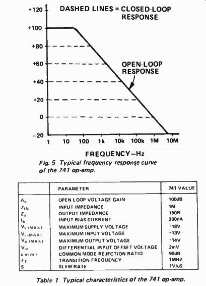
Fig. 5 Typical frequency response curve of the 741 op-amp.
Table 1 Typical characteristics of the 741 op-amp.
SLEW RATE. As well as being subject to normal bandwidth limitations, op-amps are also subject to a phenomenon known as slew rate limiting, which has the effect of limiting the maximum rate of change of voltage at the output of the device. Slew rate is normally specified in terms of volts per microsecond, and values in the range 1V/us to 10V/us are common with most popular types of op-amp. One effect of slew rate limiting is to make a greater bandwidth available to small output signals than is available to large output signals.
THE 741 OP-AMP.
Early types of i.c. op-amp, such as the well known 709 type, suffered from a number of design weaknesses. In particular, they were prone to a phenomenon known as INPUT LATCH-UP, in which the input circuitry tended to switch into a locked state if special precautions were not taken when connecting the input signals to the input terminals, and tended to self-destruct if a short circuit were inadvertently placed across the op-amp output terminals. In addition, the op-amps were prone to bursting into unwanted oscillations when used in the linear amplifier mode, and required the use of external frequency compensation components for stability control.
These weaknesses have been eliminated in the type 741 op-amp. This device is immune to input latch- up problems, has built-in output short circuit protection, and does not require the use of external frequency compensation components. The typical performance characteristics of the device are listed in Table 1.
The type 741 op- amp is marketed by most i.c manufacturers, and is very readily available Fig. 6 shows the two most commonly used forms of packaging of the device Throughout this chapter, all practical circuits are based on the standard 8- pin dual- in- line ( D.I.L. or DIP) version of the 741 op-amp.
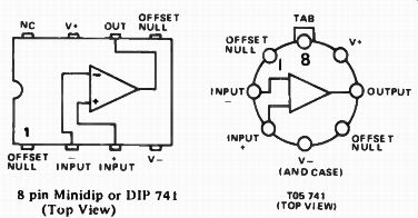
Fig. 6 Outlines and pin connections of the two most popular 741 packages.
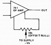
Fig. 7 Method of applying offset nulling to the 741 op-amp.
The 741 op-amp can be provided with external offset nulling by wiring a 10k pot between its two null terminals and taking the pot slider to the negative supply rail, as shown in Fig. 7 Having cleared up these basic points, let's now go on and look at a range of practical applications of the 741 op-amp.
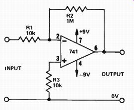
Fig. 8a x100 inverting d.c. amplifier.
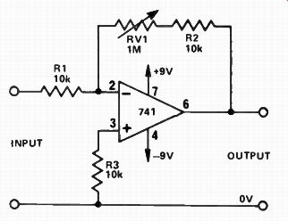
Fig. 8b Variable gain (x1 to x100) inverting d.c. amplifier.
BASIC LINEAR AMPLIFIER PROJECTS.
(Figs. 8 to 11). Figs. 8 to 11 show a variety of ways of using the 741 in basic linear amplifier applications.
The 741 can be made to function as an inverting amplifier by grounding the non- inverting input terminal and feeding the input signal to the inverting terminal.
The voltage gain of the circuit can be precisely controlled by selecting suitable values of external feedback resistance. Fig 8a shows the practical connections of an inverting d.c. amplifier with a pre-set gain of x100 The voltage gain is determined by the ratios of R, and R7, as shown in the diagram.
The gain can be readily altered by using alternative R1 and/ or R, values If required, the gain can be made variable by using a series combination of a fixed and a variable resistor in place of R7, as shown in the circuit of Fig. 8b, in which the gain can be varied over the range xl to x100 via R VARIATIONS
A variation of the basic inverting d.c. amplifier is shown in Fig. 9a. Here, the feedback connection to R, is taken from the output of the R3-R, output potential divider, rather than directly from the output of the op- amp, and the voltage gain is determined by the ratios of this divider as well as by the values of R1 and ...
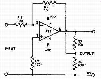
Fig. 9a High impedance x100 inverting d.c. amplifier.
... R2. The important feature of this circuit is that it enables R,, which determines the input impedance of the circuit, to be given a high value if required, while at the same time enabling high voltage gain to be achieved.
741 COOKBOOK
The basic inverting d.c. amplifier can be adapted for a.c. use by simply wiring blocking capacitors in series with its input and output terminals, as shown in the x100 inverting a.c. amplifier circuit of Fig. 9b.
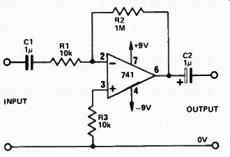
Fig. 9b x100 inverting a.c. amplifier.
NON-INVERTING ... The amp can be made to function as a non-inverting amplifier by feeding the input signal to its non-inverting terminal and applying negative feedback to the inverting terminal via a resistive potential divider that is connected across the op-amp output. Fig. 10a shows the connections for making a fixed gain (x100) d.c. amplifier.
The voltage gain of the Fig. 10a circuit is determined by the ratios of R, and R2. If R2 is given a value of zero the gain falls to unity, and if R, is given a value of zero the gain rises towards infinity ( but in practice is limited to the open-loop gain of the op-amp). If required, the gain can be made variable by replacing R2 with a ...
INPUT OUTPUT
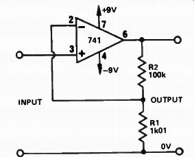
Fig. 10a Non-inverting x100
d.c. amplifier.
... potentiometer and connecting the pot slider to the inverting terminal of the op-amp, as shown in the circuit of Fig. 10b The gain of this circuit can be varied over the range x1 to x100 via R,
... AND RESISTANCE TO INPUTS
A major advantage of the non-inverting d.c. amplifier is that it has a very high input resistance. In theory, the input resistance is equal to the open-loop input resistance (typically 1M) multiplied by the open-loop voltage gain (typically 100 000) divided by the actual circuit voltage gain. In practice, input resistance values of hundreds of megohms can readily be obtained.
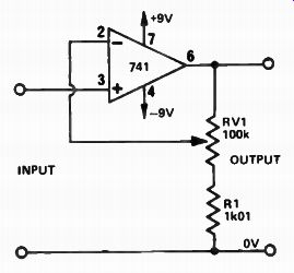
Fig. 10b Non-inverting variable gain (x1 to x 100) d.c. amplifier.
BLOCKING OUT
The basic non- inverting d.c. circuit of Fig. 10 can be modified to operate as a.c. amplifiers in a variety of ways. The most obvious approach here is to simply wire blocking capacitors in series with the inputs and outputs, but in such cases the input terminal must be d.c. grounded via a suitable resistor, as shown by 13 3 in the non-inverting x100 a.c. amplifier of Fig. 11a. If this resistor is not used the op-amp will have no d.c. stability, and its output will rapidly drift into saturation.
Clearly, the input resistance of the Fig. 11a circuit is equal to R,, and R. , must have a relatively low value in the interest of d.c. stability This circuit thus loses the non-inverting amplifier's basic advantage of high input resistance.
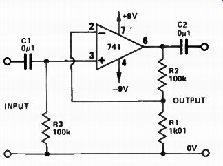
Fig. 11a Non-inverting, high input-impedance, x100 a.c. amplifier.
DRIFTING INTO STABILITY
A useful development of the Fig. 11a circuit is shown in Fig. 11b. Here, the values of R1 and R2 are increased and a blocking capacitor is interposed between them At practical operating frequencies this capacitor has a negligible impedance, so the voltage gain is still determined by the ratios of the two resistors.
Because of the inclusion of the blocking capacitor, however, the inverting terminal of the op-amp is subjected to virtually 100% d.c. negative feedback from the output terminal of the op-amp, and the circuit thus has excellent d.c. stability. The low end of R, is connected to the C3-R, junction, rather than directly to the ground line, and the signal voltage appearing at this point is virtually identical with that appearing at the non-inverting terminal of the op-amp'
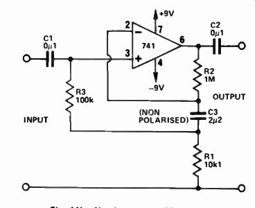
Fig. 11b Non-inverting x100 a.c. amplifier.
Consequently, identical signal voltages appear at both ends of 13,, and the apparent impedance of this resistor is increased close to infinity by bootstrap action.
This circuit thus has good d.c. stability and a very high input impedance In practice, this circuit gives a typical input impedance of about 50M. VOLTAGE FOLLOWER PROJECTS (Figs. 12 to 13). A 741 can be made to function as a precision voltage follower by connecting it as a unity-gain non- inverting amplifier. Fig. 12a shows the practical connections for making a d.c. voltage follower. Here, the input signal is applied directly to the non-inverting terminal of the op-amp, and the inverting terminal is connected directly to the output, so the circuit has 100% d.c. negative feedback and acts as a unity-gain non-inverting d.c. amplifier.
The output signal voltage of the circuit is virtually identical to that of the input, so the output is said to 'follow' the input voltage. The great advantage of this circuit is that it has a very high input impedance (as high as hundreds of megohms) and a very low output impedance (as low as a few ohms). The circuit acts effectively as an impedance transformer.
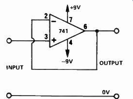
Fig. 12a d.c. voltage follower.
PRACTICE, AND ITS LIMITS
In practice the output of the basic Fig. 12a circuit will follow the input to within a couple of millivolts up to magnitudes within a volt or so of the supply line potentials. If required, the circuit can be made to follow to within a few microvolts by adding the offset null facility to the op-amp.
The d.c. voltage follower can be adapted for a.c. use by wiring blocking capacitors in series with its input and output terminals and by d.c.-coupling the non-inverting terminal of the op-amp to the zero volts line via a suitable resistor, as shown by R, in Fig. 12b. R, should have a value less than a couple of megohms, and restricts the available input impedance of the voltage follower.
LACED UP OHMS
If a very high input- impedance a.c. voltage follower is needed, the circuit of Fig. 12c can be used. Here, R1 is bootstrapped from the output of the op-amp, and its apparent impedance is greatly increased. This circuit has a typical impedance of hundreds of megohms.
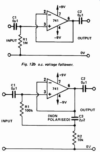
Fig. 12b a.c. voltage follower.
Fig. 12c Very high input-impedance a.c. voltage follower.
DRIVING CIRCUITS AMP-LY
The 741 op-amp is capable of providing output currents up to about 5mA, and this is consequently the current-driving limit of the three voltage follower circuits that we have looked at so far. The current-driving capabilities of the circuits can readily be increased by wiring simple or complementary emitter follower booster stages between the op-amp output terminals and the outputs of the actual circuits, as shown in Figs. 13a and 13b respectively.
Note in each case that the base-emitter junction(s) of the output transistor(s) are included in the negative feedback loop of the circuit. Consequently, the 600mV knee voltage of each junction is effectively reduced by a factor equal to the open-loop gain of the op-amp, so the junctions do not adversely effect the voltage-following, characteristics of either circuit.
The Fig. 13a circuit is able to source current only, and can be regarded as a unidirectional, positive-going, d.c. voltage follower. The Fig. 13b circuit can both source and sink output currents, and thus gives bidirectional follower action. Each circuit has a current-driving capacity of about 50mA• This figure is dictated by the limited power rating of the specified output transistors . The drive capability can be increased by using alternative transistors.
Fig. 13a Unidirectional d.c. voltage follower with boosted output (variable from 0V to +8V at 50mA.) Fig. 13b Bidirectional d.c. voltage follower with boosted output (variable from 0V to± ±8V at 50mA).
MISC AMP PROJECTS (Figs. 14 to 22)
Figs. 14 to 22 show a miscellaneous assortment of 741 amplifier projects, ranging from d.c. adding circuits to frequency-selective amplifiers.
Fig. 14 shows the circuit of a unity-gain inverting d.c. adder, which gives an output voltage that is equal to the sum of the three input voltages. Here, input resistors R, to 13, and feedback resistor R4 each have the same value, and the circuit thus acts as a unity-gain inverting d.c. amplifier between each input terminal and the output. Since the current flowing in each input resistor also flows in feedback resistor R4 , the total current flowing in R, is equal to the sum of the input currents, and the output voltage is equal to the negative sum of the input voltages. The circuit is shown with only three input connections, but in fact can be provided with any number of input terminals. The circuit can be made to function as a so-called ' audio mixer' by wiring blocking capacitors in series with each input terminal and with the output terminal.
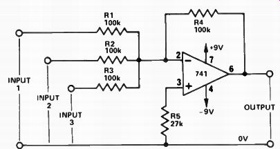
Fig. 14 Unity-gain inverting d.c. adder, or 'audio mixer'. FIG. 15 shows how
two unity-gain inverting d.c. amplifiers can be wired in series to make a precision
unity-gain balanced phase-splitter. The output of the first amplifier is an
inverted version of the input signal, and the output of the second amplifier
is a non- inverted version.
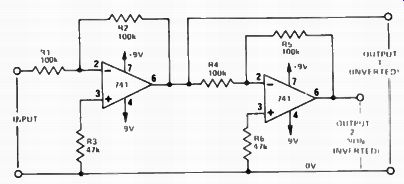
Fig. 15 Unity-gain balanced d.c. phase-splitter.
FIG. 16 shows how a 741 can be used as a unity-gain differential d.c. amplifier. The output of this circuit is equal to the difference between the two input signals or voltages, or to ere 2. Thus, the circuit can also be used as a subtractor. In this type of circuit the component values are chosen such that R , / 13 2= R4/ R3, in which case the voltage gain Av R,/ R1. The circuit can thus be made to give voltage gain if required.
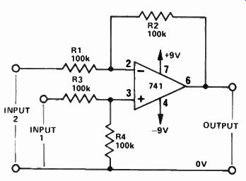
Fig. 16 Unity-gain differential d.c. amplifier, or subtractor.
FIG. 17 shows the amp can be made to act as a non-linear (semi- log) a.c. voltage amplifier by using a couple of ordinary silicon diodes as feedback elements.
The voltage gain of the circuit depends on the magnitude of applied input signal, and is high when input signals are low, and low when input signals are high. The measured performance of the circuit is shown in the table, and can be varied by using alternative R, values.
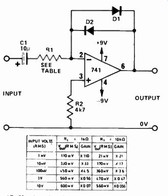
Fig. 17 Circuit and performance table of non-linear (semi-log) a.c. voltage
amplifier.
FIG. 18 shows how the 741 can be used together with a junction-type field-effect transistor (JFET) to make a so-called constant-volume amplifier. The action of this type of circuit is such that its peak output voltage is held sensibly constant, without distortion, over a wide range of input signal levels, and this particular circuit gives a sensibly constant output over a 30dB range of input signal levels.
The measured performance of the circuit is shown in the table. C, determines the response time of the amplifier, and may be altered to satisfy individual needs.
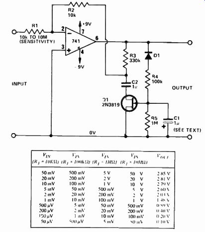
Fig. 18 Circuit and performance details of constant- volume amplifier.
ACTION TAKEN
The action of the Fig. 18 circuit relies on the fact that the JFET can act as a voltage-controlled resistance which appears as a low value when zero bias is applied to its gate and as a high resistance when its gate is negatively biased. The JFET and 13, act as a gain-determining a.c. voltage divider (via C2), and the bias to the JFET gate is derived from the circuits output via the D,-C, network.
When the circuit output is low the JFET appears as a low resistance, and the op-amp gives high voltage gain.
When the circuit output is high the JFET appears as a high resistance, and the op-amp gives low voltage gain. The output level of the circuit is thus held sensibly constant by negative feedback.
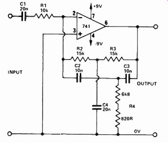
Fig. 19 1kHz tuned (acceptor) amplifier (twin- T).
741 COOKBOOK
CHOOSE YOUR FREQUENCY
The 741 op- amp can be made to function as a frequency- selective amplifier by connecting frequency-sensitive networks into its feedback loops.
Fig. 19 shows how a twin-T network can be connected to the op-amp so that it acts as a tuned (acceptor) amplifier, and Fig. 20 shows how the same twin-T network can be connected so that the op- amp acts as a notch (rejector) filter. The values of the twin-T network are chosen such that R2= R3= 2 X R 4 , and C2= C,/ 2, in which case its centre (tuned) frequency = 1 / 6.28 R2.C 2. With the component values shown, both circuits are tuned to approximately 1kHz.
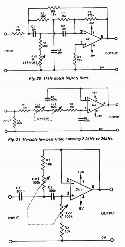
Fig. 21 Variable low-pass filter, covering 2.2kHz to 24kHz.
Fig. 20 1 kHz notch (reject) filter.
Fig. 22 Variable high-pass filter, covering 235Hz to 2.8kHz.
Finally, to complete this section, Figs. 21 and 22 show the circuits of a couple of variable-frequency audio filters. The Fig. 21 circuit is that of a low-pass filter which covers the range 2.2kHz to 24kHz, and the Fig. 22 circuit is that of a high-pass filter which covers the range 235Hz to 2.8kHz. In each case, the circuit gives unity gain to signals beyond its cut-off frequency, and gives a 2nd order response (a change of 12dB per octave) to signals within its range.
INSTRUMENTATION PROJECTS (Figs. 23 to 31)
Figs. 23 to 31 show a variety of instrumentation projects in which the 741 can be used. The circuits range from a simple voltage regulator to a linear- scale ohmmeter.
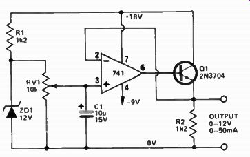
Fig. 23 Simple variable- voltage supply.
FIG. 23 shows the circuit of a simple variable-voltage power supply, which gives a stable output that is fully adjustable from 0V to 12V at currents up to a maximum of about 50mA. The operation of the circuit is quite simple. ZD, is a zener diode, and is energized from the positive supply line via R,. A constant reference potential of 12V is developed across the zener diode, and is fed to variable potential divider RV, The output of this divider is fully variable from 0V to 12V, and is fed - to the non- inverting input of the op-amp. The op-amp is wired as a unity-gain voltage follower, with Q, connected as an emitter follower current- booster stage in series with its output.
Thus, the output voltage of the circuit follows the voltage set at the op- amp input via RV,. and is fully variable from 0V to 12V. Note that the circuit uses an 18V positive supply and a 9V negative supply.
Also note that the voltage range of the above circuit can be increased by using higher zener and unregulated supply voltages, and that its current capacity can be increased by using one or more power transistors in place of Q.
FIG. 24 shows how a 741 op-amp can be used as the basis of a stabilized power supply unit ( P SU.) that covers the range 3V to 30V at currents up to 1A. Here, the voltage supply to the op-amp is stabilized at 33V via ZD,, and a highly temperature-stable reference of 3V is fed to the input of the op-amp via ZD 2.
The op-amp and output transistors Q1 -Q2 are wired as a variable-gain non- inverting d.c. amplifier, with gain variable from unity to x10 via RV,, and the output voltage is thus fully variable from 3V to 30V via RV,. The output voltage is fully stabilized by negative feedback.
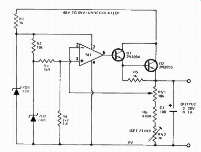
Fig. 24 3V - 30V, 0-1 amp stabilized p.s.u.
FIG. 25 shows how overload protection can be applied to the above circuit. Here, current-sensing resistor R , is wired in series with the output of the regulator. and cut-out transistor Q 3 is driven from this resistor and is wired so that its base-collector junction is able to short the base-emitter junction of the Q1 - Q2, output transistor stage.
Normally. Q., is inoperative, and has no effect on the circuit, but when P.S.U. output currents exceed 1A a potential in excess of 600mV is developed across R, and biases C1, on, thus causing C1, to shunt the base-emitter Junction of the 0,-C1, output stage and hence reducing the output current Heavy negative feedback takes place in this action, and the output current is automatically limited to 1A, even under short-circuit conditions.
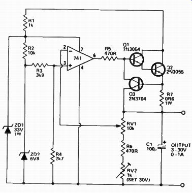
Fig. 25 3V - 30V stabilized p.s.u. with overload protection.
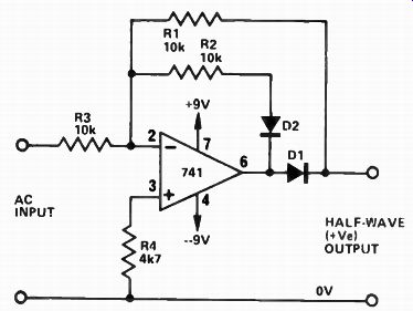
Fig. 26a Precision unity-gain half-wave rectifier.
FIG. 26a shows how a 741 can be used in conjunction with a couple of silicon diodes as a precision half- wave rectifier. Conventional diodes act as imperfect rectifiers of low-level a.c signals, because they do not begin to conduct significantly until the applied signal voltage exceeds a ' knee' value of about 600m V. When diodes are wired into the negative feedback loop of the circuit as shown the ' knee' voltage is effectively reduced by a factor equal to the open- loop gain of the op-amp, and the circuit thus acts like a near- perfect rectifier The overall voltage gain of the Fig. 26a circuit is dictated by the ratios of R1 and R, to R3, as in the case of a conventional inverting amplifier, and this circuit thus gives a gain of unity The circuit can be made to act as a precision half-wave a.c. / d.c. converter by designing it to give a voltage gain of 2.22 to give form-factor correction, and by integrating its rectifier output, as shown in Fig. 26b.
Note that each of the Fig. 26 circuits has a high output impedance, and the outputs must both be fed into loads haying impedances less than about 1M
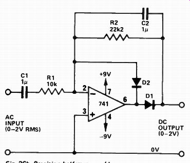
Fig. 26b Precision half- wave a.c./d.c. converter.
FIG. 27 shows how op-amp can be used as a high-performance d.c. voltmeter converter, which can be used to convert any 1V f.s.d. meter with a sensitivity better than 1k / V into a voltmeter that can read any value in the range 1mV to 10V f.s.d. at a sensitivity of 1M / V• The voltage range is determined by the R, value, and the table shows some suitable values for common voltage ranges.
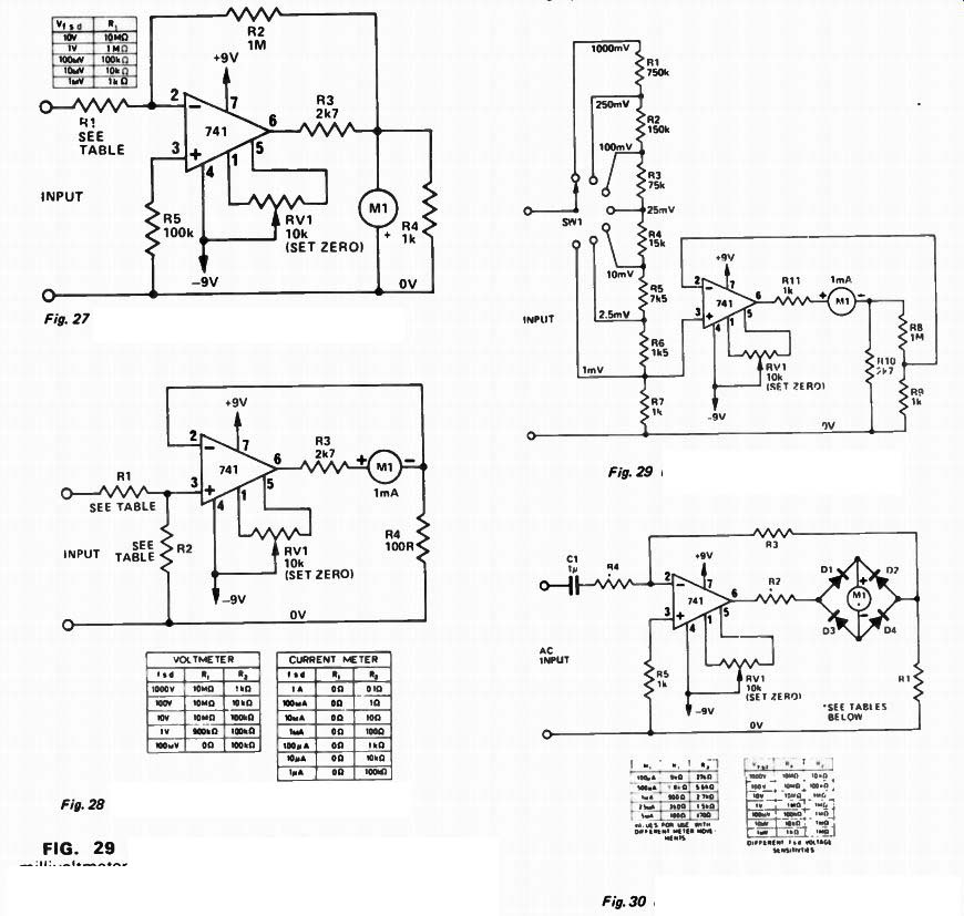
FIG. 28 shows a simple circuit that can be used to convert a 1 mA f.s.d. meter into a d.c voltmeter with any f.s.d. value in the range 100mV to 1000V, or into a d.c. current meter with any f.s.d. value in the range 1 uA to 1A. Suitable component values for different ranges are shown in the tables.
Fig. 27 High-performance d.c. voltmeter converter.
Fig. 28 Simple d.c. voltage or current meter.
FIG. 29 shows the circuit of a precision d.c. millivoltmeter, which uses a 1 mA f.s.d meter to read f.s.d. voltages from 1mV to 1000mV in seven switch-selected ranges.
FIG. 30 shows the basic circuit of a precision a.c. volt or millivolt meter. This circuit can be used with any moving-coil meter with a full scale current value in the range 100uA to 5mA, and can be made to give any full scale a.c. voltage reading in the range 1 mV to 1000mV. The tables show the alternative values of R, and R, that must be used to satisfy different basic meter sensitivities, and the values of R3 and R4 that must be used for different f.s.d. voltage sensitivities.
HOME OHM
Finally, to conclude, Fig. 31 shows how the 741 op-amp can be used in conjunction with a 1mA f.s.d. meter to make a linear- scale ohmmeter that has five decade ranges from 1k to 10M.
The circuit is divided into two parts, and consists of a voltage generator that is used to generate a standard test ...
Fig. 29 Precision d.c. millivoltmeter.
Fig. 30 Precision a.c. volt/millivolt meter.
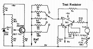
Fig. 31 Linear-scale ohmmeter.
Test Resistor
... voltage, and a readout unit which indicates the value of the resistor under test.
The voltage generator section of .the circuit comprises zener diode ZD,, transistor Q,, and resistors R, to R,. The action of these components is such that a stable reference potential of 1V is developed across R,, but is adjustable over a limited range via RV,. This voltage is fed to the input of the op-amp readout unit. The op-amp is wired as an inverting d.c. amplifier, with the 1mA meter and RV, forming a 1V f.s.d. meter across its output, and with the op-amp gain determined by the values of ranging resistors 13 5 to R, and by negative feedback resistor R. Since the input to the amplifier is fixed at 1V, the output voltage reading of the meter is directly proportional to the value of R., and equals full scale when R. and the ranging resistor values are equal.
Consequently, the circuit functions as a linear-scale ohmmeter.
CALIBRATION
The procedure for initially calibrating the Fig. 31 circuit is as follows: First, switch the unit to 10k range and fix an accurate 10kU resistor in the R. position. Now adjust RN/ , to give an accurate 1V across R., and then adjust RV, to give a precise full scale reading on the meter. All adjustments are then complete, and the circuit is ready for use.
MISCELLANEOUS 741 PROJECTS
The 741 op-amp can be used as the basis of a vast range of miscellaneous projects, including oscillators and sensing circuits. Four such projects are described in this final section.
FIG. 32 shows how the 741 op-amp can be connected as a variable-frequency Wien-bridge oscillator, which covers the basic range 150Hz to 1.5kHz, and uses a low-current lamp for amplitude stabilization. The output amplitude of the oscillator is variable via RV, and has a typical maximum value of 2.5V r.m.s. and a t.h.d. value of 0.1%. The frequency range of the circuit is inversely proportional to the C1 - C, values. The circuit can give a useful performance up to a maximum frequency of about 25kHz.
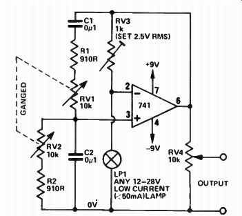
Fig. 32 150Hz - 1.5k Hz Wien-bridge oscillator.
Fig. 33 shows how either a 741 or a 709 op-amp can be connected as a simple variable-frequency square-wave generator that covers the range 500Hz to 5kHz via a single variable resistor. (The circuit produces a good symmetrical waveform.)
The frequency of oscillation is inversely proportional to the C, value, and can be reduced by increasing the C, value, or vice-versa. The amplitude of the square wave output signal can be made variable, if required, by wiring a 10k variable potential divider across the output terminals of the circuit and taking the output from between the pot slider and the zero volts line.
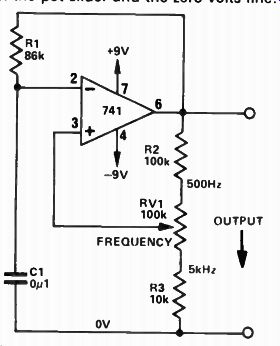
Fig. 33 Simple 500Hz - 5kHz square wave generator.
FIGS. 34 and 35 show a couple of useful ways of using the 741 op-amp in the open-loop differential voltage comparator mode. In each case, the circuits are powered from single-ended 12V supplies, and have a fixed half- supply reference voltage applied to the non-inverting op-amp terminal via the R1 - R, potential divider and have a variable voltage applied to the inverting op-amp terminal via a variable potential divider.
The circuit action is such that the op-amp output is driven to negative saturation (and the relay is driven on) when the variable input voltage is greater than the reference voltage. Conversely, the op-amp output is driven to positive saturation (and the relay is cut off) when the variable input voltage is less than the reference voltage.
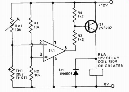
Fig. 34 Precision frost or under temperature switch can be made to act as
a fire or over temperature switch by transposing Ri and TH1 positions.
FROSTY RECEPTION
The Fig. 34 circuit is that of a precision frost or under-temperature switch, which drives the relay on when the temperature sensed by thermistor TH, falls below a value pre-set via RV,. The circuit action can be reversed, so that it operates as a fire or over-tempera ture switch, by simply transposing the RV, and the TH, positions. In either case, TH, can be any negative-temperature-coefficient thermistor that presents a resistance in the range 9009 to 9k9 at the required trip temperature.
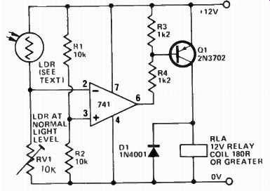
Fig. 35 Precision light-activated switch can be made to act as a dark-activated
switch by transposing R1 and LDR positions.
LIGHT WORK
The Fig. 35 circuit is that of a precision light-activated switch, which turns the relay on when the illumination level sensed by light- dependent resistor LDR exceeds a value pre-set by RV, The circuit action can be reversed so that the relay turns on when the illumination falls below a pre-set level by simply transposing the RV, and LDR positions. In either case, the LDR can be any cadmium-sulphide photocell that presents a resistance in the range 9009, to 9k9 at the desired switch-on level.