This remarkable IC is quite different to run-of-the-mill op-amps as it has a "control - pin that varies the device's transconductance as the current into this input is varied. These circuits illustrate various ways to use the device - from an original manuscript by UK correspondent, Tim Orr.
THE CA3080 IS KNOWN as an operational transconductance amplifier (OTA). This is a type of op-amp, the gain of which can be varied by means of a control current, ( Imic). The device has a differential input, a control input known as the 'amplifier bias input' and a current output. It differs in many respects from conventional op-amps and it is these differences that can be used to realize many useful circuit blocks.
Voltage controlled amplifier
The CA3080 can be used as a gain con trolling device. A useful circuit is shown in Figure 1. The input signal is attenuated by R1, R2 such that a 20 mV peak to-peak signal is applied to the input terminals. If this voltage is much larger, then significant distortion will occur at the output. In fact, this distortion is put to good use in the triangle-to sinewave converter. (Figure 3, but we're jumping the gun). The gain of the circuit is controlled by the magnitude of the current I_ABC. This current flows into the CA3080 at pin 5, which is held at one diode voltage drop above the - Vcc rail. If you connect pin 5 to 0 V, then this diode will get zapped (and so will the IC!). The maximum value of I_ABC permitted is 1 mA and the device is 'linear' over four decades of this current. That is, the gain of the CA 3080 is 'linearly' proportional to the magnitude of the I_ABC current over a range of 0.1 uA to 1 mA. Thus, by controlling I_ABC, we can control the signal level at the output.
The output is a current output which has to be 'dumped' into a resistive load (R5) to produce a voltage output. The output impedance seen at IC1 pin 6 is 10k (R5), but this is 'unloaded' by the voltage follower (IC2) to produce a low output impedance.
The circuit involving IC3 is a precision voltage-to-current converter and this can be used to generate Luc. When Vin (control) is positive, it linearly controls the gain of the circuit. When it is negative, 'ABC is zero and so the gain is zero.
This type of circuit is known by several names. It is a voltage controlled amplifier, ( VCA), or an amplitude modulator, or a two quadrant multiplier.
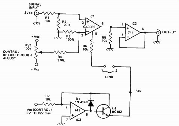
Figure 1 A voltage controlled amplifier. Gain is varied by varying RV1. You
can modulate a signal passing through the amplifier by joining the link and
applying a modulating signal to the input of IC3 ( at R7). This sort of circuit
is also known as a two quadrant multiplier'.
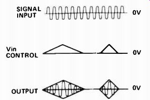
Figure 2. Illustrating the operation of the voltage controlled amplifier shown in Figure 1.
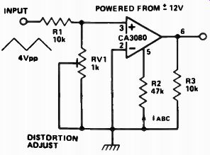
Figure 3. This circuit will convert a triangle wave to a sinewave with a resultant distortion of around 1.8%.
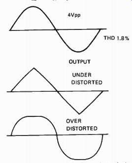
Figure 4. The output of the Figure 3 circuit should be adjusted (by RV1) to
produce the waveform shown at top.
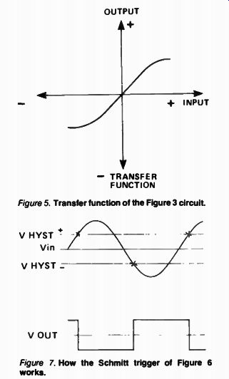
Figure 5. Transfer function of the Figure 3 circuit.
ABC CONTROLS HYSTERESIS LEVELS AND OUTPUT LEVEL
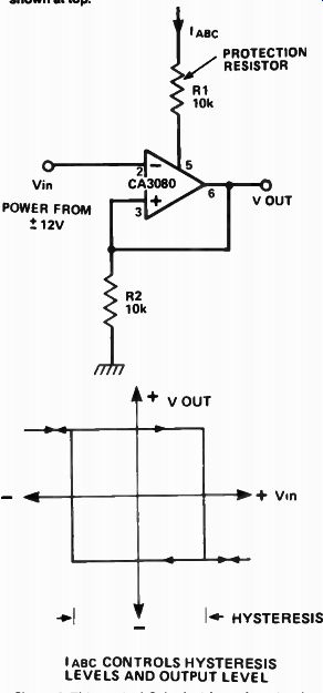
Figure 6. This sort of Schmitt trigger Is not only simple but you can specify the hysteresis levels as well!
Figure 7. How the Schmitt trigger of Figure 6 works.
One problem that occurs with the CA3080 is that of the 'input offset voltage'. This is a small voltage difference, or 'offset', between its input terminals. When there is no signal in put and the control input is varied, a voltage similar to the control input will appear at the output. By adjusting RV1 it is possible to null out most of this control breakthrough.
The effect of modulating Vin ( control) is illustrated in Figure 2.
Triangle to sinewave converter
By overloading the input of a CA3080 it is possible to produce a 'sinusoidal' transfer function. That is, if a triangle waveform of the correct magnitude is applied to the CA3080 input, the output will be distorted in such a way as to produce a sinewave approximation.
In the circuit shown (Figure 3), RV1 is adjusted so that the output waveform resembles a sinewave. I tested this circuit using an automatic distortion analyzer and found the sinewave distortion to be only 1.8%, mostly third harmonic distortion which, for such a simple arrangement, seems very reasonable indeed. This could be used to produce a sinewave output from a triangle/square wave oscillator.
The result of varying RV1 is illustrated in Figure 4 and the transfer function of the circuit is shown in Figure 5.
Schmitt trigger
Most Schmitt trigger circuits prove to be very complicated when it comes to calculating the hysteresis levels.
However, by using the CA3080 these calculations are rendered trivial, plus there is the added bonus of fast operation. The hysteresis levels are calculated from the simple equation, VHYST = (IBC X R2)
The output squarewave level is in fact equal in magnitude to the hysteresis levels. The circuit operation is as follows ( referring to Figure 7): Imagine the output voltage is high.
The output voltage will then be equal to (R2 x Imi(') which we will call + VHYST. If VIN becomes more positive than + VHYST, the output will start to move in a negative direction, which will increase the voltage between the input terminals which will further accelerate the speed of the output movement. This
===========
Lab Notes
---------- SELECTED DATA ON THE 3080
-------------- General description The 3080 is a programmable transconductance block intended to fulfill a wide variety of variable gain applications. The 3080 has differential inputs and high impedance push-pull outputs.
The device has high input impedance and its transconductance (gm) is directly proportional to the amplifier bias current (I_ABC).
High slew rate together with programmable gain make the 3080 an ideal choice for variable gain applications such as sample and hold, multiplexing, filtering, and multiplying.
Electrical characteristics, 3080 (Note 1).
Parameter Forward Transconductance (gm)
Peak Output Current Peak Output Voltage Positive Negative Amplifier Supply Current Common Mode Rejection Ratio Common Mode Range Input
Resistance Open Loop Bandwidth Slew Rate Conditions Over Specified Temp. Range RL = 0, lAsc = 5uA RL = ° AL = ° Over Specified Temp. Range RL = 5uA 'ABC 500uA RL= 5uA IABC 5°C> uA Unity Gain Compensated
Features
• Slew rate (unity gain compensated): 50 V/us
• Fully adjustable gain: 0 to gm RL limit
• Extended gm linearity
• Flexible supply voltage range: +/- 2 V to +/- 18 V
• Adjustable power consumption Absolute maximum ratings Supply Voltage 3080 +/-18 V Power Dissipation 250 mW
Note 1: These specifications apply or Vs = + / - 15 V and TA = 25°C, amplifier bias current (I_ABC) = 500uA, unless otherwise specified.
Differential Input Voltage +/-5 V Amplifier Bias Current ( lAsc) 2 mA DC Input Voltage +/V s to - Vs Output Short Circuit Duration Indefinite
Internal circuit of the 3080
----------------------------
============
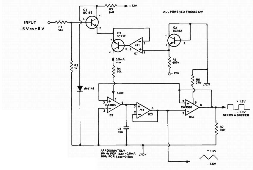
--- Figure 8. This voltage controlled oscillator has a square and a tri angle output. By varying the input between - 5 V and + 5 V, the output frequency can be varied over the range 10 Hz to 10 kHz. Note that 01 and 02 should be a matched pair.
... is known as regenerative feedback and is responsible for the Schmitt trigger action. The output snaps into a negative state at a voltage equal to ...
-(R2 x 'Am)
... which is designated as -VHysr. Only when VIN becomes more negative than
-VHYST will the output change back to the + VHYST state.
The Schmitt trigger is a very useful building block for detecting two discrete voltage levels and finds many uses in circuit designs.
Voltage controlled oscillator
By using two CA3080s and some 741 op-amps it is possible to make an oscillator, the frequency of which is voltage controllable. This unit finds many applications in the fields of electronic music production and test equipment.
The circuit (Figure 8) has been given a logarithmic control law, that is, the frequency of operation doubles for every volt increase in the control voltage. This makes it ideal for musical applications where linear control voltages need to be converted into musical intervals (which are logarithmically spaced) and also for audio testing where frequencies are generally measured as logarithmic functions.
One CA3080, IC2, is an integrator.
The I_ABC current that drives this IC is used to either charge or discharge C1.
This produces triangular waveforms which are buffered by IC3, which then drives the Schmitt trigger IC4. The hysteresis levels for this device are fixed at +/- 1.5 V, being determined by R6 and R7.
The output of the Schmitt trigger is fed back in such a way as to control the direction of motion of the integrator's output. If the Schmitt output is high, then the integrator will ramp upwards and vice versa.
Imagine that the integrator is ramping upwards. When the integrator's output reaches the upper hysteresis level, the Schmitt will flip into its low state, and the integrator will start to ramp downwards. When it reaches the low hysteresis level the Schmitt will flip back into its high state. Thus the integrator ramps up and down in between the two hysteresis levels.
The speed at which it does this, and hence the oscillating frequency, is determined by the value of IAsc for IC2.
- 15V
The larger the current, the faster the capacitor is charged and discharged.
Two outputs are produced, a triangle wave (buffered) from IC3 and a square wave (unbuffered) from IC4. If the squarewave output is loaded, then the oscillation frequency will change so a buffer is advisable.
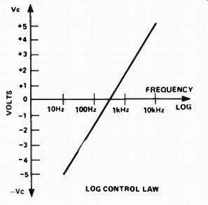
Figure 9. Voltage versus frequency characteristic of the Figure 9 circuit.
The log, law generator is composed of Q1, 2,3 and IC1. Transistors Q1 and Q2 should be matched so that their base emitter voltages (Vbe) are the same for the same emitter current, (50uA). Matching these devices to within 5 mV is satisfactory, although unmatched pairs could be used. When matching transistors, take care not to touch them with your fingers. This will heat them up and produce erroneous measurements.
Transistor Q2 is used to produce a reference voltage of about - 0.6 V, which is connected to IC1 pin 3. This op-amp and Q3 is used to keep the emitter of Q1 at the same voltage of -0.6 V. The input control voltage is attenuated by R1, R2 such that a + 1 V increase at the input produces a change of only + 18 mV at the base of Q1. however, the emitter of Q1 is fixed at -0.6 V, so the current through Q 1 doubles. (It is a property of transistors that the collector current doubles for every 18 mV increase in Vbe). The emitter current of Q1 flows through Q3 and into IC2, thus con trolling the oscillator frequency. It is possible to get a control range of over 1000 to 1 using this circuit. With the values shown, operation from 10 Hz to 10 kHz is achieved. Reducing C1 to in will increase the maximum frequency to 100 kHz, although the waveform quality may be somewhat degraded.
Changing C1 to 1uF (non-polarized) will give a minimum frequency of 0.1 Hz.
Fast comparator
The high slew rate of the CA3080 makes it an excellent fast voltage comparator and a circuit is shown in Figure 10.
When pin 2 of IC1 is more positive than Vref, the output of IC1 goes negative and vice versa. Vref can be moved around so that the point at which the output changes can be varied. As long as the input sinewave level is quite large (1 V say) then the output can be made to move at very fast rates indeed. however, care must be taken to avoid overloading the inputs. If the differential input voltage exceeds 5 V, then the input stage breaks down and may cause an undesired output to occur.
One use of a fast comparator is in a tone burst generator. A circuit is shown in Figure 11. This device produces bursts of sinewaves, the burst starting and finishing on axis crossings of the sinusoid. The CA3080 is configured here as a voltage comparator, used to detect these axis crossings and to produce a square wave output which then drives a binary divider (IC3). The divider produces a 'divide by sixteen' output which is high for eight sinewave cycles and then low for the next eight.
This signal is then used to gate ON and OFF the sinewave.
The gate mechanism is a pair of transistors which short the sinewave to ground when the divider output is high and let it pass when the divider output is low. The resulting output is a toneburst.
However, if the comparator is not V_in
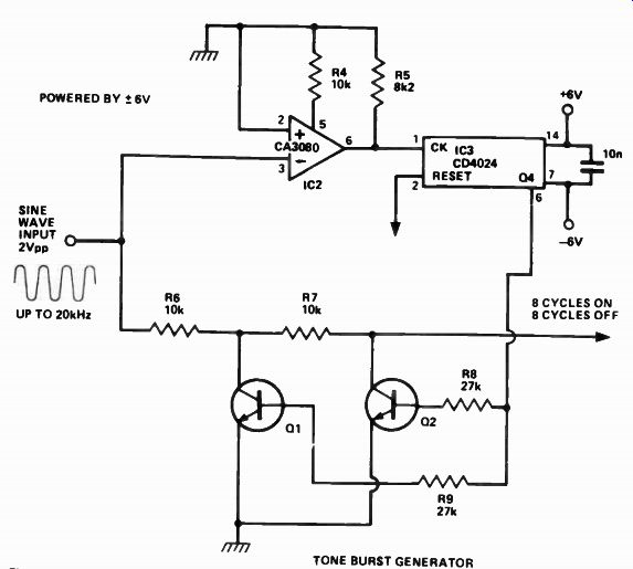
Figure 11 A fast comparator is used in this tone burst generator, producing
eight cycles of tone with eight cycle breaks starting and finishing at on-axis
crossings.
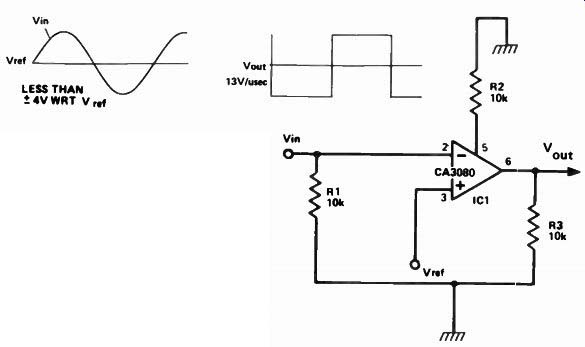
Figure 10. Example of a fast comparator.
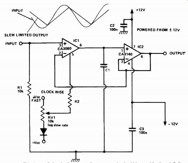
Figure 12. This slew rate limiter circuit produces a linear ramp on signals
which exceed the slew rate limit, the output amplitude stopping when it reaches
the signal level.
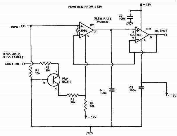
Figure 13. A typical application of the slew rate limiter is this sample and
hold circuit.
... very fast then there will be a delay in generating the gate and so the tone burst will not start or finish on axis crossings.
Using the circuit shown, operation up to 20 kHz is obtainable.
Slew limiter
The current output of a CA3080 can be used to produce a controlled slew limiter. By connecting the output current to a capacitor, the output voltage-cannot move faster than a rate given by:
Slew Rate = I_ABC Volts per sec.
C1 Note that ' ABC determines the slew rate and as I_ABC is a variable then so is the slew rate.
A suitable circuit is shown in Figure 12. The output voltage is buffered by a voltage follower, IC2. This is a MOSFET op-amp which has a very high input impedance, which is necessary to minimize the loading on C1.
When an input signal is applied to IC1 the output tries to move towards this voltage but its speed is limited by the slew rate. Thus, the output produces a linear ramp which stops when it reaches the input signal level.
Sample and hold
A typical application of the slew limiter circuit is in a sample and hold circuit.
The circuit in Figure 13 could be termed an analog memory. When the control voltage is high, the circuit will 'remember' or ' hold' the input voltage level present at the time. The result is shown in Figure 14.
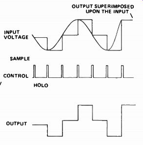
Figure 14. Illustrating the operation of the sample and hold circuit of Figure
13.
In this circuit, IABc is either hard ON (sample) or completely OFF (hold). In the sample mode, the output voltage quickly adjusts itself so that it equals the input voltage. This enables a short sample period to be used.
In the HOLD mode, I_ABC is zero and so the voltage on C 1 should remain fixed.
Such circuits are used in music synthesizers (to remember the pitch), in analog-to-digital converters and many other applications.
A multiplier/modulator
The CA3080 is basically a two quadrant multiplier, that is, it has two inputs, one of which can accept bipolar signals (positive and negative going) - the inverting or the non-inverting input - the other can only accept a unipolar signal -- the control input, pin 5.
Whilst a two-quadrant multiplier is very useful in a wide variety of applications, a four-quadrant multiplier has extra advantages. For example, apart from amplitude modulation, it can perform frequency doubling and ring modulation. See Figure 16. Now, a four quadrant multiplier has two inputs, both of which can accept bipolar signals.
An example of a four-quadrant multiplier is a frequency converter in a radio receiver. The familiar diode ring mixer is another example of a four-quadrant multiplier.
The circuit in Figure 15 is fairly similar to that of the two-quadrant multiplier shown in Figure 1. This circuit has several important differences.
Figure 16 Illustrating the various operations of the four quadrant multiplier of Figure 15.
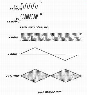
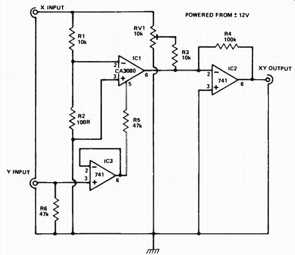
Figure 15. This Multiplier/modulator can be used to produce a Dalek' voice
when working as a ring modulator. It can also be used as a frequency doubler.
A 741 op-amp, IC3, is used to generate I_ABC in such a way that its input, the ' Y' input, can go both positive and negative.
Thus, the Y input is bipolar.
When Y is at zero volts (no input) and there is a signal on the X input the desired output (X x Y) should be zero. This is achieved by adjusting RV1 so that the signal via IC1 (this is inverted) is exactly cancelled out by that via R3.
Now, when Y is increased positively, a non-inverted value of X is produced at the output and, when Y is increased negatively, an inverted value of X is produced. When Y is zero, so is the output. This is known sometimes as ring modulation.
If a speech signal is connected to the X input and an audio oscillator to the Y input, the resulting sound is that of a ‘Dalek'. Also, if a sinewave is connected to both the X and Y inputs, the XY product is a sinewave of twice the frequency.
This is known as a frequency doubler, but it will only work with sinewaves.
For more theoretical information on four-quadrant multipliers, especially the variable transconductance type, see "Operational Amplifiers" (second edition), by G.B. Clayton, published by Newnes-Butterworths and available in Australia through Butterworths, 586 Pacific Highway, Chatswood NSW 2067. (02)412-3444.
Single pole filter/wah wah
The guitar `wah wah' effects unit employs a filter which can be manually 'swept' across the middle of the audio frequency range, generally from around 500 Hz to 5 kHz or so, producing the peculiar 'wah wah' sound.
A single pole, voltage-controlled, low pass filter can be constructed using a CA3080 as a current-controlled resistor. The circuit is shown in Figure 17.
A simple, low pass RC filter configuration is employed, the controllable 'R' is the CA3080 and the 'C' is C1. Varying I_ABC varies the amount of current drive to Cl. This circuit configuration would normally be a slew limiter, except that the signal level to the input of the CA3080 is kept deliberately low (R1 and R2 form a 100:1 attenuator) so that the IC operates in its linear mode. This enables it to look like a variable resistor.
When this resistor is varied, the break frequency of the filter also varies.
By applying some positive feedback around the filter ( R6, C2) it is possible to produce a peaky filter response. The peak actually increases with frequency, producing the wah-wah effect.
The circuit as shown can be swept from about 400 Hz at the lower extreme to about 4 kHz at the upper extreme.
See Figure 18.
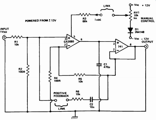
Figure 17. A guitar wah-wah unit can be made with a swept frequency single
pole filter.
Figure 18. How the single pole filter affects the frequency response of the signal passed through the wah-wah unit.
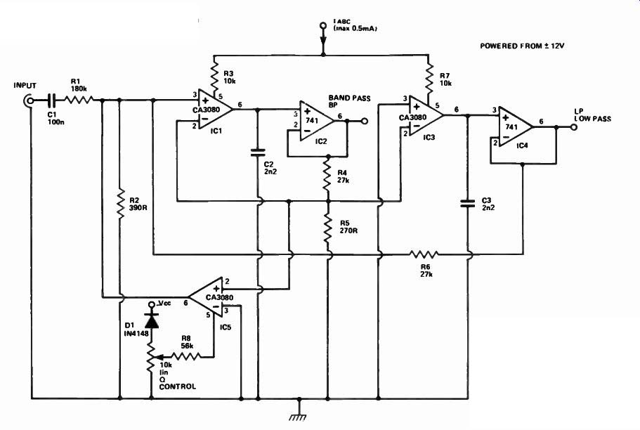
Figure 19. A swept frequency, voltage controlled dual filter. This circuit
includes a band pass and a low pass filter, both of which can be simultaneously
swept over the range 7 Hz to 7 kHz, approximately.
The Q can be varied by means of the 10k ' 0 Control' potentiometer.
Voltage controlled filter A standard dual integrator filter can be constructed using a few CA3080s. By varying I_ ARC, the resonant frequency can be swept over a 1000 to 1 range. I C1 and IC3 are two current-controlled integrators. IC2 and IC4 are voltage followers which serve to buffer the high impedance outputs of the integrators. A third CA3080 ( C5) is used to control the Q factor of the filter. Q factors as high as 50 can be obtained. The resonant frequency of the filter is linearly proportional to 'AB(' and hence this unit is very useful in electronic music production.
There are two outputs, a low pass and a band pass response. Minimum frequency is around 7 Hz to 10 Hz, upper frequency is around 7 kHz or so.
Changing C2 and C3 will alter the upper and lower frequency limits.
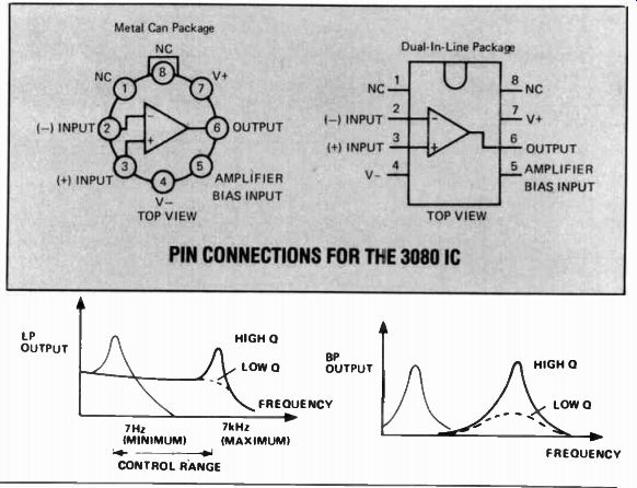
Figure 20. Illustrating the operation of the filters in the Figure 19 circuit.
PIN CONNECTIONS FOR THE 3080 IC