Design your next filter the easy way - this article by Tim Orr shows you how.
THERE ARE THREE main types of filter -- low-pass, band-pass, and high-pass. Each does more or less what its name implies. A low pass filter passes all frequencies below the so-called ' roll off' point and increasingly blocks all frequencies above this point. A band-pass filter passes all frequencies above a lower 'roll-off' point and below a higher roll-off point. A high-pass filter passes all frequencies above the roll-off point.
Firstly, consider the simple low-pass filter shown in Fig. 1a. The frequency response ( shown in Fig 1b) is nearly flat until the break point shown as fb.
Above this point the response rolls off at 6 dB/octave. The break point is defined as the frequency where the resistance equals the capacitive reactance. At this point the output is attenuated to 0.707 (-3 dB) of the input. Although the resistance equals the capacitive reactance, the output is not half of the input. It is the vector sum of the two and hence is 0.707 of the input.
As the frequency response is a complex curve it is commonly approximated by a straight line. Such a line is called an asymptote ( Fig. 1c). Note the frequency response graph uses logarithmic scales, octave or decades along the frequency axis, and dBs along the vertical axis representing output voltage divided by input voltage.
Phase shift with respect to frequency is often plotted as in Fig. 1d. Phase and frequency response plots are also known as Bode diagrams and are most useful in showing a filter's performance.
Note that for the low-pass filter of Fig. 1a, phase shift starts at 0°, is 45° at fb and approaches 90° as frequency approaches infinity. This is not an active filter. It is made up from passive components and its output cannot be loaded substantially without changing its performance.
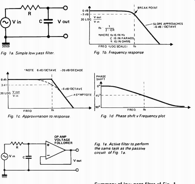
Fig. 1a Simple low pass filter
Fig. 1c. Approximation to response.
Fig. 1b. Frequency response
Fig. 1d Phase shift y Frequency plot.
Fig. 1e. Active filter to perform the same task as the passive circuit of Fig. 1a.
Summary of low pass filter of Fig. 1
Figure le shows the same filter in active form, the op amp being used as a voltage follower serving only to isolate the filter's output. This configuration is known as a first order filter - the expression 'first order' being an indication of the roll-off slope.
When a steeper slope is required, a higher order filter ( that is, one with more elements) must be used. These are dealt with later.
Passing Highs
The simple high-pass filter shown in Fig 2a is the complement of the low-pass filter - the elements have simply been interchanged. Hence the complementary curves of Fig 2b. Note the break point and roll-off slope are similar.
Passing bands
A simple band-pass filter is shown in Fig 3a. Although it uses an inductor this is only to illustrate the band-pass theory.
The frequency response ( Fig 3b) is symmetrical, rolling off at 6 dB/octave on either side of its peak. This filter is called a second order filter because it has two reactive sections ( L and C). The C produces the +6 dB/octave portion of the slope, the L the -6 dB portion. The response of the filter peaks, and the slopes become much steeper where these two slopes meet.
The sharpness of the peak determines the quality of the filter ( Q). Resonance occurs at the frequency known as the centre frequency - shown on our drawing as fc.
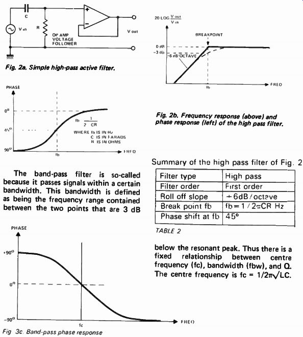
Fig. 2a. Simple high-pass active filter.
The band-pass filter is so-called because it passes signals within a certain bandwidth. This bandwidth is defined as being the frequency range contained between the two points that are 3 dB below the resonant peak. Thus there is a fixed relationship between centre frequency (fc), bandwidth ( fbw), and Q. The centre frequency is fc = 1/277VLC.
Fig. 2b. Frequency response (above) and phase response (left) of the high pass filter.
Summary of the high pass filter of Fig. 2
Filter type High pass Filter order First order Roll off slope 4-6dB/ ocme
Break point fb fb= 1 / 2 pi R Hz Phase shift at fb 45°
TABLE 2
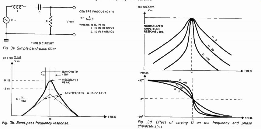
Fig. 3a. Simple band-pass filter
Fig. 3b. Band-pass frequency response.
Fig. 3c Band-pass phase response.
Fig. 3d. Effect of varying 0 on the frequency and phase characteristics
This is only approximate as it assumes that the value of R is relatively low.
As R decreases, the Q increases. Thus R has the effect of damping the resonances, and as it approaches zero ohms, Q approaches infinity.
The phase shift is shown in Fig 3c.
As this filter is a second order structure the total phase movement will be twice that of a first order structure, i.e. 180°. Figure 3d shows the phase and frequency responses for different values of Q. Note that a high Q has a very rapid rate of change of phase, a low Q has only a slow rate of change.
Time response
Band-pass filters have a time response as well as a frequency response. When an impulse is applied to a band-pass filter it rings ( Fig 3e). The filter oscillates at the centre frequency ( fc), the amplitude of oscillations decaying exponentially with time. The ringing time Tr is the time taken for the oscillations to decay to 37% of their initial value.
Ringing time is related to Q and fc by the following equation:
Tr = Q/2 pi fc
In practice it may prove difficult accurately to measure the Q of a high-Q filter because the band-width is narrow.
However if the filter can be made to ring a reasonably accurate measurement of Q can be obtained by measuring Tr and fc.
Notch filters
Another common type of filter is the band-reject or notch filter. There are many ways of building these, one way is shown in Fig 4. The input signal is subtracted from the band-pass output.
By adjusting Ra with respect to R, complete cancellation can be obtained at fc. Thus the centre frequency of the band-pass filter is the centre frequency of the notch. The depth of this notch can be varied by altering the value of Ra.
Very deep notches are possible: 50 dB being readily obtainable. As the Q of the band-pass filter is increased so is the Q of the notch filter. Note that Ra must be adjusted for each value of Q. Filter orders Consider the ideal filter shown in Fig 5a. Its response is flat right up to the break frequency with frequencies above fb attenuated to zero. It looks really...
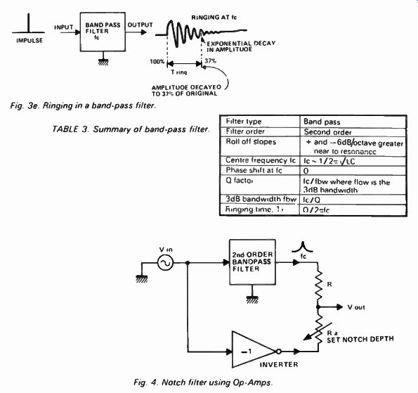
Fig. 3e. Ringing in a band-pass filter.
TABLE 3. Summary of band-pass filter
Fig. 4. Notch filter using Op-Amps.
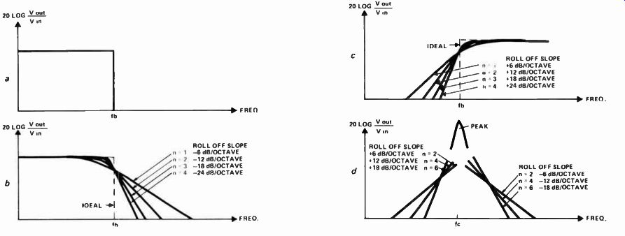
Fig. 5a. Ideal low-pass response; b,c. Examples of maximally flat filter responses;
d. Effect upon band-pass filter of increasing order number.
... good but in real life filters like this don't exist! There is nevertheless a frequent need to design filters with very steep roll-off slopes. This is achieved by designing filters with lots of sections - thus increasing the filter order.
Each reactive element in a filter increases the filter order by one, therefore a low pass active filter with three capacitors is known as a third order filter and will have an ultimate roll-off of three times 6 dB/octave i.e. 18 dB/octave.
Unfortunately there is more to designing a third order low-pass filter than just sticking three first order circuits in line astern. That merely results in a very soggy curve! The filter should be flat in the pass band, then it should turn over and rapidly assume its roll-off slope. Examples of maximally flat filters are shown in Figs 5b and 5c.
The effect of order number on a band-pass filter is shown in Fig 5d.
Later in this article circuit diagrams and design charts are shown for various filter types and order numbers. It might seem that to persuade a filter to approach its ideal response all that is needed is to increase the order number.
This is of course so -- but there are problems in obtaining components of sufficient accuracy. An eighth order filter for example needs components having values within 1% - possible with resistors but virtually impossible for capacitors.
Filter Shape
The type of filter required to do a certain job will depend on what parameters are most important. Three basic characteristics must be considered ( high pass and low-pass only).
1. Good transient response
2. Maximum flatness within the pass- band
3. Steep roll-off slope.
Filters have been categorized into three basic types for simplicity.
BESSEL FILTER: phase changes almost linearly with frequency, useful for systems where a good transient response is required - such as joining all the little pulses on the output of a digital-to analog convertor. Very poor initial roll off.
BUTTERWORTH FILTER: This has the flattest pass band possible. Its two other parameters are a compromise - a reasonable overshoot and a fairly fast initial roll-off.
CHEBYSHEV FILTER: This has a small amount of ripple in its pass band, a very fast initial roll off but a poor transient response.
Rolling your own In all the examples which follow the filters have been designed for operation at 1 kHz. To change the operating frequency resistor/s RF must be scaled accordingly ( note: resistors RD are not changed). For example if the filter is required to operate at 250 Hz then RF must be multiplied by 1 ÷N . Figure 7 shows a first order low pass filter.
Figure 8a, b, and c shows second, third and fourth order filters.
The total design procedure is as follows:
1. Decide which type of filter is required -- low, band-pass or high.
2. In the case of low or high-pass decide which type of response is required, Bessel, Butterworth of Chebyshev.
3. Decide what filter order is needed.
This will lead you to a particular order filter with components shown scaled for 1 kHz.
4. Scale the resistors RF accordingly.
5. Build and test the filter.
As an example let us design an audio scratch filter having a break frequency of 7.5 kHz and an attenuation of more than 20 dB at 15 kHz.
The first decision is type of response required. A roll-off of more than 20 dB/ octave is quite steep and so the Bessel filter is ruled out. The Chebyshev has poor transient response and we'd hear it ringing at 7.5 kHz. So we're left with the Butterworth.
Next comes filter order. Third order gives - 18 dB/octave: this is not enough.
Fourth order gives - 24dB/octave. So a fourth order Butterworth filter it is.
Break frequency is 7.5 kHz so resistors RF and RF2 must be divided by 7.5. This gives the following rather funny values - RF1 = 1k42, RF2- 1k42, RD1 = 5k9,
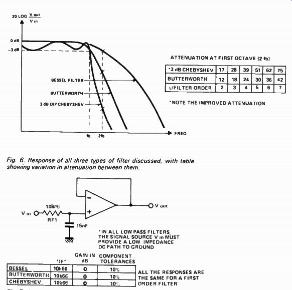
Fig 6 Response of all three types of filter discussed, with table showing
variation in attenuation between them

Fig. 7. A general circuit for a first order low-pass filter.
RD2 = 48k7, C = 15 nF with component tolerances of 5%.
We must now fit preferred values to our theoretically derived numbers.
Resistor RD2 can be 47k. RD1 6k2 (just over the limit of tolerance). Resistors RF1 and RF2 are a bit of a problem. The solution is to use the nearest 1% tolerance resistor or use 1K5.
This will lower the break frequency by 6% but as this is an audio filter it won't matter too much.
Figure 9 provides design data for high-pass filters. The design procedure is exactly the same as for the low-pass designs.
A few problems may occur with the final results. One is that these filters have a voltage gain in their pass band - so you might find that although you have the required frequency response there is unexpected signal gain.
This may cause some problems with op amp band-width. As a rule of thumb, op amps should have 10 to 100 times more band-width than the product of the filters' maximum operating frequency multiplied by the individual stage gain of each section. If the op amp runs out of band-width or introduces a phase shift the filter won't work properly. For the examples given if you use a 741 as the op amp the frequency limit is about 10 kHz. With an LM 318 the limit can go right out to 200 kHz.
Another problem is the range of values of RF. If RF is too small large currents flow from the op amp and this may affect filter performance. If RF is too large there may be hum pick-up, and dc offset voltages due to bias currents. So keep RF between 1 k and 100 k. If RF appears to need to exceed this range scale the capacitor accordingly.
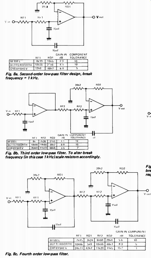
Fig. 8a. Second-order low-pass filter design, break frequency = 1 kHz.
Fig. 8b. Third order low-pass filter. To alter break frequency (in this case 1 k Hz)scale resistors accordingly.
Fig. 8c. Fourth order low-pass filter.
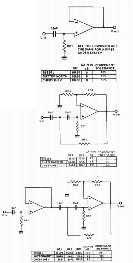
Fig. 9. From the top: First, second and third order high-pass filters, break
point 1 kHz. Final roll-off is 6, 12, and 18 d8/octave respectively.
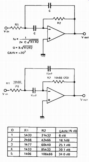
Fig. 10. A multiple feedback bandpass filter. The centre circuit is normalized
for 1 kHz. The table is the design table for this circuit. To change the design
frequency change R1 and R2 by an equal factor.
Band-pass filters
Several second order band-pass filters can be cascaded to produce a different response shape, which, like those discussed earlier for low and high-pass filters, can be optimized to give maximum roll-off or maximum pass- band flatness. Such filters do however tend to be difficult to design and so only second order filters will be discussed.
Figure 10 shows a simple band-pass filter known as a multiple feedback circuit. This circuit can provide only low orders of Q ( up to about 5). It will probably oscillate if designed to provide higher Q. Note that a high Q implies a large gain at centre frequency. Care must therefore be taken to ensure that the op amp has sufficient band-width to cope.
The design chart is shown in Fig 10 -- once again all values are shown for 1 kHz. The design procedure is to first choose the Q factor and then perform the frequency scaling. For instance if the centre frequency is to be 250 Hz then multiply both R1 and R2 by four.
If a high C1 is required then you must use a multiple op amp circuit such as the 'state variable' or ' Bi - Quad' circuits shown later. Both circuits can achieve Qs as high as 500. State-variable filter A state- variable filter is shown in Fig 11.
This filter has three main features:
1. It can provide a stable high Q
2. It is readily tuned
3. It is versatile, providing band-pass, low-pass and high-pass outputs all at the same time.
The Q of this filter is determined by the ratio of resistors RA and RB where RA/RB=3Q-1. The resonant frequency fc is 1/2 pi 13C Note that there are two Cs and two RFs in the circuit. If the filter is to be tunable then both RFs should be changed by an equal amount ( the RFs can of course be a dual potentiometer). Note too that Q and fc are independent of each other so as the resonant frequency is changed Q remains constant - and vice versa.
The requirements placed on the op amps in the state-variable filter are less than those for the multiple feedback circuit. The op amps need only have an open loop gain of 30 at the resonant frequency. Suppose we have a Q of 100 and an fc of 100 kHz. Then the open loop gain is 300, the frequency is 10 kHz and so the gain band-width product needed is 3 MHz.
Fig. 1 lb. The state variable filter is called a universal filter because it can give band-, low and high-pass outputs - as shown above. Note that all these responses are second order in nature.
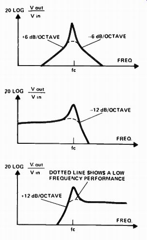
Fig. 11a. The state variable filter.
When using a high Q, care must be taken with signal levels. The gain of the filter is +CI at resonance so if you are filtering a 1V signal with a Q of 100 you could expect a 100 V output signal! National Semiconductor manufactures an active filter IC which is a four .op amp network which can be used to make up state-variable filters with Qs of up to 500 and frequencies to 10 kHz. The device is designated AF 100.
Bi - Quad filter
Figure 12 shows a Bi - Quad active filter.
It looks very similar to the state-variable filter but the minor changes cause it to behave quite differently. Unlike the state-variable filter it has only a band-pass and a high-pass output. The resonant frequency is 1 fc - 27rCR F V
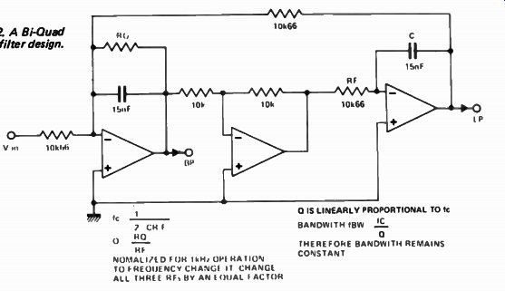
Fig. 12. A Bi-Quad active filter design.
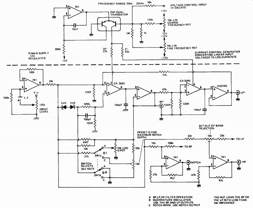
Fig. 13. The state variable filter can also be made to oscillate (as above).
It has a variable resonant frequency, and so becomes a variable frequency oscillator.
This circuit produces two low-distortion sinusoids in phase- quadrature: i.e.
sine and cosine waveforms.
Notch filters
Two notch filters were shown earlier in this article. These worked by mixing a band-pass signal with the original or by mixing the low and high-pass outputs.
There are however many other methods of producing a notch response.
The twin-T circuit shown in Fig 14 is very interesting -- a notch response is obtained using resistors and capacitors only. However as this is purely a passive device only a low Q can be obtained.
The circuit is not used a great deal -- perhaps because no less than six components determine its notch frequency.
However it is of interest to note that when the twin-T is placed in the feed back loop of a high-gain amplifier a band-pass response will be obtained. If R is made variable it is possible to move the center frequency, although in doing so the Q varies. This effect has been exploited as the basis of many wah-wah effects units!
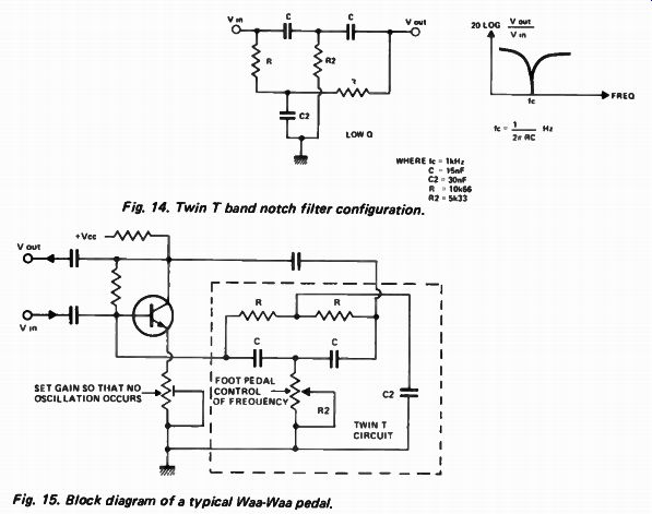
Fig. 14. Twin T band notch filter configuration. Fig. 15. Block diagram of a
typical Waa-Waa pedal.
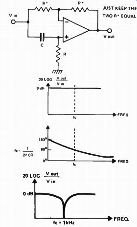
Fig. 16. All-pass filter. At the top is the circuit for such a device. Its
frequency and phase responses are shown below it, with the obtainable notch
at the bottom.
All-pass filter
Another way of obtaining a notch is the all- pass filter shown in Fig 16. The frequency response might at first sight make this the most useless of all possible filters - it's flat! However the circuit produces a phase shift which goes from 180°, through 90° at fc – to 0 °. By cascading two such filters the phase shift is doubled: if we then mix the phase-delayed signal with the original a notch response is obtained.
This is because at fc the two signals have the same magnitude but opposite phase and so cancel out.
If the notch is to be tunable the RC time constants must be variable. Just one R may be varied if a small range is required -- otherwise vary both Rs.
Comb filter
Several notches can be produced by cascading notch filters. This type of filter is called a comb filter. Every notch in the comb requires two all- pass filters.
The notches can be made to move up and down in frequency by making the Rs variable. This method is used to produce the 'phasing' effect used by rock groups.
Figure 17 shows a small section of such a unit. Here a CMOS chip is used to provide a matched set of six MOS-FETS. A common voltage controls the MOSFET's channel resistance. Thus as the control voltage varies so do the six MOSFET resistors - and the three notches move along the frequency axis in unison.
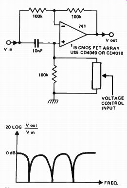
Fig. 17. One section of a comb filter. The response produced by the full (six
times above) circuit is shown below the circuit.
delay times.
Another type of comb filter is shown in Fig 18. Here a time delay line is used instead of a phase delay line. This produces a large number of notches linearly spread along the frequency axis, their spacing being determined by the
A bucket-brigade device may be used to implement the time delays (which can of course be made variable). This type of filter is known as a flanger and is used to generate high quality phasing effects. An even more impressive sound can be produced by adding feedback around the delay line: this produces a multi- peak, high-Q filter which makes very interesting 'musical' sounds when swept through its range.
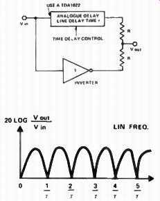
Fig. 18. Alternative method of producing a comb filter using a Mullard delay
line.
Variable tuning
A common requirement is for a variable centre or cut-off frequency. This causes problems with filters of orders more than two simply because it is difficult to obtain potentiometers with more than two ganged sections. Lots of companies make them but just try to buy one when it's needed! One solution is to use mark/space ratio modulation ( Fig 19). This has the advantage of offering continuously variable control over a range of about 100:1. Lots of sections may be used and they'll all track. As an example an eighth order four transmission-gates/ pack variable frequency filter can be made using a couple of CD4016s. Note though that: -
1. The switching waveform must be several times higher in frequency than the highest frequency to be filtered.
2. More circuitry, to generate the switching waveform is required.
3. Switching noise tends to be generated.
Audio circuits
Active filters are widely used in equalizing audio signals in applications varying from simple tone controls in hi-fi systems to parametric equalizers in recording studios. Figure 20 shows a commonly used tone control with bass and treble functions. Cut and lift ranges are 20 dB. More flexible control can be obtained by using a multi- band graphic equalizer such as that described as a constructional project in ETI's June 1977 issue.
Testing
Once the process of designing active filters has been reduced to a simple procedure, testing should be made as simple as possible too. The most basic method is to use a swept sinewave oscillator ( Fig 21).
An XY oscilloscope is used to display frequencies logarithmically against amplitude (displayed linearly). The ideal display would be log amplitude but this is hard to do. The beauty of this method of testing is that the display is in real time so any changes appear instantly on the oscilloscope. If high Qs or rapid roll-offs at low frequencies are involved, then the sweep time will have to be reduced, otherwise the effects of ringing will 'time smear' the display. The harmonic distortion of the sinewave, can be quite large ( 0.5 to 2.0%) without causing too much of a display problem for most filter designs.
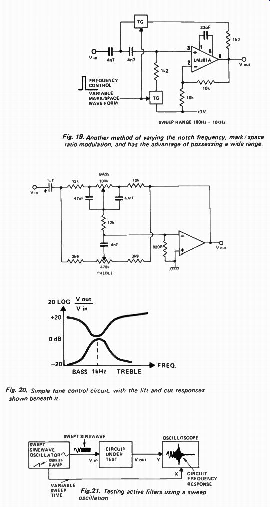
Fig. 19. Another method of varying the notch frequency, mark/space ratio modulation,
and has the advantage of possessing a wide range.
Fig.
20. Simple tone control circuit, with the lift and cut responses shown beneath
it.