Inherently rugged, CMOS logic has many advantages over other logic families - high noise immunity and uncritical power requirements are but two. This, the second article in this four part series deals primarily with quad switches.
THE 4016A QUAD BILATERAL switch consists of four transmission gates of the type discussed in the previous article, each with its own control input. Each switch also has a signal input and output (although these are interchangeable). When the control input is held high the input to output path behaves like a pure resistance of about 300R but when it is low the equivalent value is of the order of 10^9 ohms at low frequency, even with fairly low supply voltages. It is impossible to give all the data which might be necessary for diverse applications - data sheets from a manufacturers may be required by the more adventurous experimenters.
In any case the pin diagram in Fig. 1 should now be self explanatory.
It should be appreciated that the output impedance of the switch is fairly high and so for low signal distortion, a load greater than 10 k- ohm is necessary.
Using a high supply voltage ( 10-15 V) also helps to achieve this end. The gates will pass signals above the 10 MHz mark but as the frequency becomes higher, crosstalk between the switches (and distortion) will inevitably increase. It should be fairly clear how complicated switching systems may be realised but Fig. 2 has been included to guide constructors along the right lines.
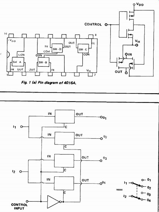
Fig. 1 (a) Pin diagram of 4016A.
Fig. 2. DPDT electronic switch realised using a single 4016 and an inverter.
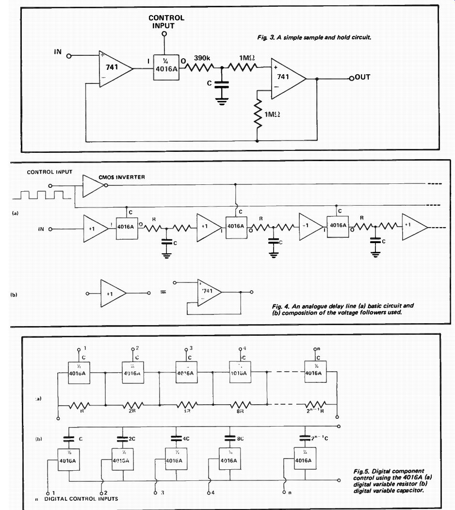
Fig. 3. Fig. 4. An analog delay line (a) basic circuit and (b) composition of
the voltage followers used. Fig. 5. Digital component control using the 4016A
(a) digital variable resistor (b) digital variable capacitor.
ANALOG APPLICATIONS
Many uses of this device in audio equipment have already appeared in constructional articles in this magazine and so it is to two slightly less obvious applications that we shall turn now.
Figure 3 shows a sample and hold unit.
When the control input is high the output tracks the input, but when it goes low the output remains frozen at the value it was at the instant of transition. The operation of the circuit is generally self evident and it may be regarded as two voltage followers, one consisting of two op-amps with the output following the input, the other is just the second op-amp which follows the voltage stored on the capacitor. It is advisable to take care with the layout, as with all op-amp circuits, due to the huge open loop gain of these devices.
The value chosen for C is a compromise between "slewing rate," that is the rate at which the circuit tracks a sudden change of input, and "holding ability" which is the length of time the circuit will hold a signal without unreasonable decay. To give some sort of guide, for a 10 kHz square wave to the control input, a 0.01µF capacitor seems to optimize the performance. The value of the resistors is also worth experimenting with.
An extension of the sample and hold concept is the analog delay line which is shown in its basic form in Fig. 4. The sequence of amplifiers and gates can be extended to any desired length to achieve a longer delay, the only limitation being that in extreme cases the control lines may need to be buffered. It should be observed that alternate stages of the circuit are driven by an identical clock waveform and so the circuit works by shifting the voltage on alternate capacitors during alternate clock phases. The value of the passive components and the clock frequency will have to be optimized for specific applications, low frequencies give long delays but high distortion.
DIGITAL COMPONENT SELECTION
There are a few fairly straight-forward uses of the 4016A in digital component selection which we will mention here because, in certain fields, they are very useful. Figure 6 shows how to produce digitally controlled resistance and capacitance networks which will vary the magnitude of the quantity in question from its basic value up to 2^ - 1 times that amount, where " n" is the number of gates and binary control bits.
The resistor network can be used to produce a digitally gain controlled amplifier by placing it in the feedback loop of an op-amp and this can be used as a staircase generator - as well as to produce more interesting waveforms.
One application of the digital capacitor is to produce a digitally controlled sweep generator by using it as the capacitor in one of the multivibrators we discussed last month.
Any type of component may be switched in and out of circuit by the 4016A. One possibility that is useful in some circumstances is to use the information on filter design in "Electronics - it's easy" to produce digital filters of different descriptions.
The main thing to remember when using all these ideas is that the impedance of the component that is being switched must, at the desired frequency of operation, be large compared to the won of the 4016A gates.
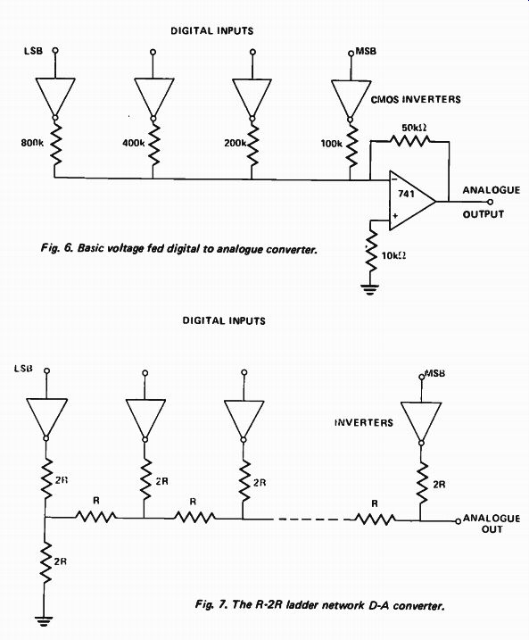
Fig. 6. Basic voltage fed digital to analog converter.
Fig.
7. The R-2R ladder network D-A converter.
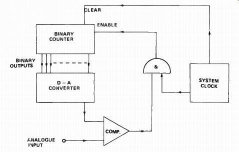
Fig. 8. Outline of A-D converter using 'Binary ramp' method. The binary counter
counts up to the required value so that the output is correct during only part
of the cycle.
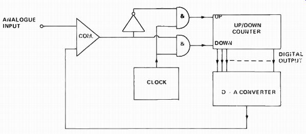
Fig. 9. A continuous counter type A-D converter. The clock just prevents the
system oscillating at high frequency.
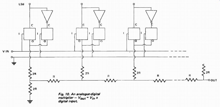
Fig. 10. An analog-digital multiplier - V out = Vio x digital input.
D/A and A/D TECHNIQUES
The next use of the quad bilateral switch that we are going to consider is digital to analog conversion, but first we are going to look at the subject of conversion on its own. Figure 6 shows a D-A converter of the type known as a weighted resistor network. The working of this circuit is easy to see and the reason it is practical in so simple a form in CMOS is that the high and low output levels from a simple gate are within a few millivolts of the supply line thus providing accurate voltage levels to the summing resistors. This simple form has disadvantages, one of which will become immediately apparent if you consider the diversity of resistor values required for an eight or nine bit version.
It is for this reason that the R-2R network shown in Fig. 7 is more popular for most applications. It is difficult to explain how this configuration works without becoming involved in mathematics but it becomes fairly clear if a three bit version is written down with the voltages in and analyzed.
The basic idea for one sort of A/D converter or encoder as they are often called is shown in the block diagram of Fig. 8. This variety is called a binary ramp encoder and is similar to the ramp integration method often encountered in modified form in digital measuring equipment. The principle of operation of our binary version is that a binary counter counts up from zero until it reaches the equivalent of the analog input. Contrast this approach with the continuous counter method outlined in Fig. 9. This provides a continuous approximation to the input and is thus generally more useful for continuously monitoring a single channel of information. It would be an advantage in many cases to have the counters working in BCD for ease of readout but this leads to complications. Finally on this subject it should be pointed out that these are circuits for experimentation and are unlikely to be directly applicable to any specific situation. They have been included because of the ease with which they may be realised in CMOS compared, say, to TTL.
A/D MULTIPLIER
As far as digital to analog conversion is concerned ( using the 4016A) we can take the idea a little further. What in fact we do ( Fig. 10) is to use an arbitrary analog voltage to feed the resistor ladder and so we multiply this input by the digital input and produce an analog result. This "hybrid multiplier" is an interesting circuit, particularly because the analog input voltage may be ac thus producing several interesting waveforms and, on a more serious note, it may find application in hybrid computing experiments. We shall now leave the 4016A having, it is hoped, suggested some of the slightly less obvious uses of this versatile IC. Our next subject is flip-flops - and we shall assume that the reader is familiar with the working of these devices, and so the discussion will begin with the pinout diagrams in Fig. 11. The first two are standard, dual edge - triggered devices with "D" and J- K" type data inputs respectively. No doubt it is known that the "D" variety will divide the input frequency by two if "Q" is connected to "D" whereas the "J- K" type toggle, as this behavior is called, when both "J" and " K" are held high.
The set and reset inputs operate asynchronously ( ie. independently of the clock) forcing the device into the "Q" = 1 and "Q" = 0 states respectively.
These inputs operate when taken high in contrast to most TTL because TTL inputs rest high when disconnected whereas CMOS inputs must never be allowed to "float" anyway. Both the 4016A and the 4027A will operate up to about 8 MHz.
The last device in Fig 11 ( the 4042A) is a quad data latch of the sort often used for temporary storage of BCD digits in applications like frequency meter displays. If the polarity input is held low then the "Q" output follows the " D" input in each latch when the clock is also low. But on the rising edge of the clock pulse the outputs are isolated and retain the data present at that moment. When the polarity input is high all this works the other way round.
The clock inputs to all these devices should have rise times of 5ps or less ( at Vdd = 10 V). Flip-flops on their own have uses in control circuitry and counters. If you wish to produce a counter to count through an odd sequence ( a Gray code for example) it is advisable to find out about Karnaugh maps and associated techniques which aid the design process considerably. The standard form for such counters is a sequence of flip-flops whose inputs are derived from the outputs of the others by a few simple logic gates. As far as simple binary is concerned the required set-up is shown in Fig. 12 but we shall have a lot more to say on the subject of counters in general later.
The other main application of flip-flop is in shift registers. A shift register is a sequence of flip-flops so interconnected (see Fig 13) that on a clock pulse the content of each device is transferred to the next one down the line. The register so formed is referred to as a static device because, unlike some MOS devices available, data is not lost if it is not shifted for some length of time. One modification to the basic device is to provide inputs and outputs to individual flip-flops in the chain and in this form shift registers have many applications in serial-to- parallel and parallel-to-serial data conversion. This though is another subject which must wait until a little later in our discussions.
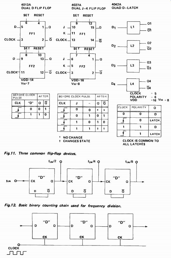
Fig. 11. Three common flip- flop devices. Fig. 12 Basic binary counting chain
used for frequency division.
Fig.
13. Principle of shift register. The content of each "cell" is
shifted one place to the right on the rising edge of the clock pulse.