Operational amplifiers are of wide application, but some of their design considerations are not clearly spelled out in the textbooks. Here a few mysteries are explained.
By Bernard B. Daien
In Part II we gave the formulae for the voltage gain of an op amp in both the inverting, and the non-inverting configurations. Since we are going to build on these basic formulae, they are repeated in Figure 1, along with tables showing how the gain varies with different ratios of resistors in the feedback loop.
If you compare the gains of the inverting, and the non-inverting amplifiers, for the same values of feedback resistors, you will notice that the non inverting gain is always 1 more than the inverting gain. Therefore we can rewrite the gain for the non-inverting amplifier as, "R_f/R_in + 1", and, if you compare this gain, to the gain obtained using the same ratio of resistors, in the negative feedback formula in Part 1 of this article, you will notice that they are the same.
Adding and Subtracting . . .
Stated simply, the general feedback formula for negative feedback, works with single input amplifiers, such as audio amplifiers, and also with the non-inverting input op amp. The inverting op amp has a gain of one less than the general formula. Since the inverting and the non-inverting inputs have different gains, if we attempt to use both inputs simultaneously, as a differential amplifier, the op amp will not work properly.
It will give us an output, despite common mode rejection built into the op amp! In order for the op amp to function as a differential amplifier, a voltage divider has to be connected between the non inverting input and the signal generator, in order to reduce the gain of the non inverting input down to the gain of the inverting input. When this is done, the gain of the inverting and the non-inverting inputs is identical, and the op amp can be used as a true differential input amplifier. This is shown in Figure 2, along with the calculations used for the resistors required.
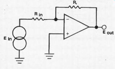
Fig. 1A. The inverting amplifier.
Rf = feedback resistor
R in = Series input resistance (including signal generator internal resistance!).
Voltage gain = ---/- R in
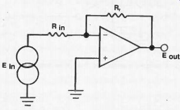
Fig. 1B. The non-inverting amplifier.
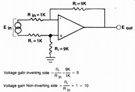
Fig. 2. The differential amplifier. But, there is a voltage divider in the
non-inverting side. R1 and R2, which provides a loss, so that the output of
the divider = 9/10 of the input.
Then the non-inverting gain of 10 is reduced to 9/10 x 10 = 9, and both the investing and the non-inverting sides of the amplifier have the same gain. In actual design therefore, the ratio of RR in, is always the same as the ratio R0/R,. To insure this, 1% resistors are used, and then R in = R, and R, = R, for simple and effective design calculations.
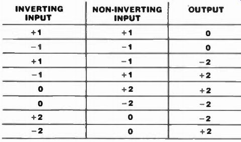
Fig. 3. Differential amplifier, input vs. output. Output versus inputs for
a differential amplifier with a voltage gain of 1 Note: If the op amp closed
loop gain had been set for 5: then the outputs shown would be multiplied by
a factor of 5
This is an algebraic Subtractor with gain as desired
Notice that in the case illustrated, the gain of the inverting input is 9, but the gain of the non-inverting input is 10, as described earlier. In order to reduce the gain of the non-inverting input to 9, from 10, we need a voltage divider that provides an output of 0.9 times the input.
Then the gain, multiplied by the divider loss, is, "10 x 0.9," which of course, equals 9. With both sides of the op amp providing a gain of nine, the inputs are "balanced" and common mode rejection is restored. This tells us that if plus one volt is applied to both inputs, the output will behave as if there is no signal at the inputs at all. This happens be cause the gains are EQUAL AND OPPOSITE. (The inputs are out of phase). But, there is more . . . Let us consider what happens if we apply plus one volt to one input, and minus one volt to the other input. In that case the output will behave as if there was two volts applied to one input, and zero volts applied to the other. Thus the differential amplifier configuration responds only to the difference between the two input terminals, and in the pro cess performs THE SUBTRACTION OF TWO SIGNALS. Let's test this by trying some input signals, in table form in Figure 3. Note that when both inputs are the same, the output is zero. With a closed loop gain of 1, if the inverting input is minus 1 volt, and the non-inverting input is plus one volt, the output is plus two volts. If you continue down the table you will quickly see that the output is always the algebraic difference (algebraic subtraction) of the two inputs.
It is easy to increase the output by using a closed loop gain greater than one, if desired.
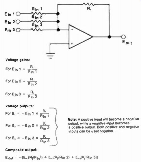
Fig. 4. The summing amplifier. (inverting) Note: A positive input will become
a negative output while a negative input becomes a positive output Both positive
and negative inputs can be used together
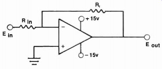
Fig. 5A. Inverting amplifier using
dual power supplies.
(For those of you who have forgotten the procedure, to subtract in algebra, you merely change the sign of the lower number, then add in algebra. In this case, change the sign of the inverting input, and add the two inputs). Now that we have pointed out that the differential amplifier can be used for algebraic subtraction, we should also note that we can do algebraic addition using the "summing amplifier," (which we already know as the inverting amplifier). This brings us to the need for some practical applications information Examine Figure 2, and the accompanying information carefully, and you will notice that the ratio of the two resistors in the feedback loop in the inverting side, is always the same as the ratio of the divider resistors in the non inverting side! This makes building a practical differential amplifier (or "sub- tractor," if you will), very simple. These resistors must be very carefully matched however, i.e., the ratio of the resistors must be very carefully matched however, i.e., the ratio of the resistors in each input must be the same. The use of 1% metal film resistors is usual, but performance can be improved by matching with a digital meter. Remember, performance is not very dependent upon the op amp, with the feedback loop closed . . . but is very dependent upon the resistors in the feedback loop.
Now let's look at the schematic for an inverter (or "summing" amplifier). Several different inputs can be fed into the inverting side of the op amp, and the output of the op amp will be the algebraic sum of the inputs, but inverted, since we are using the inverting input.
The schematic and calculations are shown in Figure 4. Notice that we can also change the gain of each individual input, if that is desired. This is taken into account in the calculations, which show each input multiplied by the resistor ratio for that input. This makes the summing circuit a very flexible one, since it can not only add, but also multiply each in put by a different factor, simultaneously! This circuit has a very useful feature, despite the number of inputs used, there is no cross-talk between them.
Thus, in audio mixing use, the various signals can be recovered in the output without cross talk. This is true because of the very low input impedance existing at the inverting input, which is the common point for all input signals, and is a virtual ground.
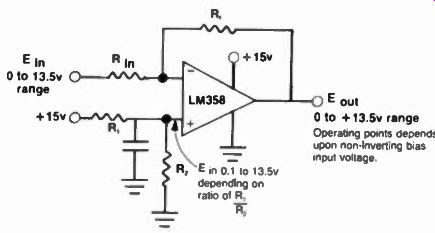
Fig. 5B. Inverting amplifier using single power supply. Note: In this circuit
the output cannot swing negative, as with dual supply operation, and the input
also cannot be driven below zero volts.
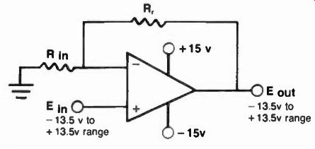
Fig. 6A. Non-inverting op-amp using dual power supplies.
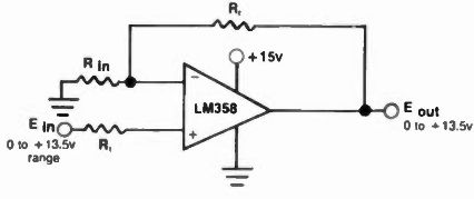
Fig. 6B. Non-inverting op-amp using single power supply.
Note: In this circuit, the output cannot swing negative, as with dual supply operation, and the input also cannot be driven below zero volts
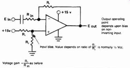
Fig. 7A. Inverting ac amplifier, single power supply.
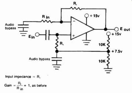
Fig. 7B. Non-inverting ac amplifier, single power supply.
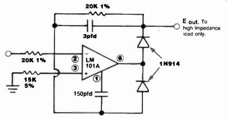
Fig. 8. A half-wave rectifier.
Notes: The output i high impedance The circuit as show operates with a negative going input and a positive going output Reversing the polarity of the diodes, reverses polarity of operation Errors are very low to 100kHz. so long as a high speed op amp is used A high impedance load should be used. preferably an emitter follower, to reduce loading effects on the high Z Output
Single supply operation
Before we go further, it should be emphasized that most op amp literature describes the basic two-power-supplies circuitry, employing a positive and a negative power supply. Recently op amps have been developed which work well with a single power supply, but there is a fundamental difference in operation with these, which is not really made clear in most literature .. . When using dual supplies, both the input and the output can be at ground potential, since the output can swing either positive or negative. When using a single supply, however, the input should be biased so that the output operating point (the quiescent level) is somewhere between ground and the available supply voltage. The output voltage can then swing up to the supply voltage and down to zero, just as is the case with discrete transistor amplifiers.
Figure 5A shows the schematic of an inverting amplifier, as used with dual power supplies. Note that the non-inverting input is at dc ground, and the output can swing either positive or negative. In Figure 58, the same inverting amplifier is set up for use with a single power supply, and the non-inverting in put is biased from the single power sup ply. The output can swing down to zero, or up to the power supply voltage, and normally stays about midway between the two. Figure 6A shows a dual supply non-inverting amplifier, while Figure 6B is the single supply configuration.
Most circuits for single supply operation are published as ac amplifiers (audio, etc.) and therefore have blocking capacitors at the input, as in Figure 7. This makes things very simple for authors, ... since the ac input signal does not create a conflict with the dc biasing. When op amps are used with a single power supply, and dc input signals, the situation becomes a little more complicated, since there is no way to avoid interaction between the dc bias, and the dc input signal.
Let's look at that another way. With a single power supply we need to bias the op amp so that the output is in the linear region ... i.e. neither saturated nor cut off. A dc input signal will then vary the dc output around the desired operating point. With dual supplies this is no problem, since the output is normally at ground (zero volts), and the in put signal, positive or negative, merely causes the output to swing + or - in accordance with the level of the input signal, the polarity of the input signal, and the gain of the amplifier.
Notice that in both the inverting and non-inverting ac coupled, single supply circuits the biasing is fed into the non inverting input, and the inverting input develops the same dc bias voltage via the feedback network. This is because of what we learned in the earlier parts of this series . . . that in an op amp operating closed loop, the voltage difference between the two inputs is always close to zero. (That applies to dc as well as ac!) So if you bias the non-inverting input, the inverting input will be driven by the feedback loop to the same potential as the non-inverting input, and both inputs of the op amp will be properly biased.
Non-linear applications
Up to this point we have been considering only applications in which the op amp is used as a linear amplifier. There are many uses for non-linear circuits, therefore we are going to consider some of these now.
As you undoubtedly already know, a diode rectifier (or detector) has a forward voltage drop of over a half a volt for silicon diodes, and over a tenth of a volt for germanium. At times this may be far too great for the use intended.
Figure 8 shows the schematic for a half wave rectifier that works at millivolts of input! (This half wave rectifier will operate to a hundred kilohertz and there fore may be used as a detector in many instances). Figure 9 is a full wave rectifier. By reversing the diodes as noted in the figure, the output of the full wave rectifier is easily reversed to produce a positive output.
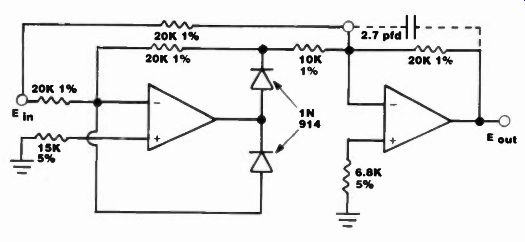
Fig. 9. A full-wave rectifier.
Note: For low speed operation. use 741, or 747 op amps For faster operation. use 1556 op amps Output is negative For positive output, reverse the diodes
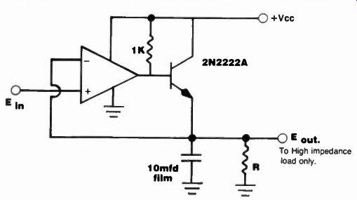
Fig. 10A. A positive peak detector.
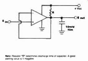
Fig. 10B. A negative peak detector.
Note: The output must see a very high resistance to avoid loading the capacitor, which holds the peak charge. It is advisable to drive into an emitter follower. Resistor "R" then determines the capacitor discharge time. A starting value for R is about 1 megohm.
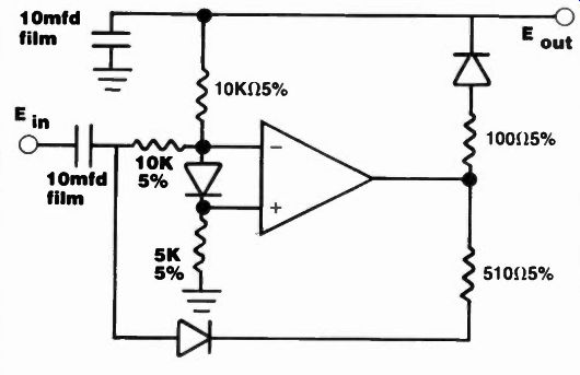
Fig. 11. A peak-to-peak detector. Note: All diodes Fairchild FD 600. Input
must be driven from a low impedance source, otherwise an internally compensated
op-amp must be used to prevent oscillation. The output is a positive dc voltage
proportional to the peak-to-peak voltage of the input waveform.
Figure 10 is a peak detector, while Figure 11 is a PEAK-TO-PEAK DETECTOR. Resistor "R" determines the discharge time of the peak voltage held by the capacitor. Changing the value of "R" changes the discharge time as desired.
There is no way to discuss op-amps without including "active filters." In the next article in this series we will talk about active filters, IC op amp failure inducing conditions, and troubleshooting IC op-amps.
It should be stated, that by convention, when the power supply for an op-amp is omitted in the schematic, it is assumed that dual power supplies are required. That convention is used in this series. Therefore, when power supplies are not shown in the schematic diagrams, dual supplies are required. (Most circuits require dual supplies. Single supply op amps are a recent development, and they require more circuit complexity).
(source: Electronic Technician/Dealer)
Also see: Operational Amplifiers, Part 1
OP Amps IV--Norton amplifiers and active filters