Last month we gave an insight into the design procedures for low level phono signals. This month the theory is put into practice with these outstanding input amplifiers. Design and development by David Tilbrook.
The preamp has been designed specifically to overcome the problem of cartridge impedance interaction. This has been achieved by separating the MM input stage into two separate active stages (see Fig. 1). The first stage consists of a single NE5534AN configured as a linear amplifier with a closed loop gain of around 8.3. The large amount of overall negative feedback increases the input impedance of the stage so that the measured input impedance is simply that of the 470k resistor, R2. Since the 5534 has a small signal bandwidth of around 10 MHz without additional compensation, the input impedance will remain unchanged over a very wide frequency range. The high input impedance of this stage would usually allow the input capacitor C2 to be conveniently small. However, for best noise performance the value must be increased substantially.
Capacitor C2 is necessary since it is not advisable to allow DC current from the first stage to flow through the cartridge. The value of C2 used here is 100uF, and this sets the lower-3 dB point well below 1 Hz. The upper -3 dB point of this stage is well above 100 kHz. An extended frequency response is necessary so that the accuracy of the RIAA equalization is not affected by frequency response variations that might otherwise occur in the first stage.

Fig. 1. Circuit of one channel of the moving magnet input stage. Note that
the RIAA equalization is incorporated in this stage.
Equal Change
In an attempt to overcome bass problems the RIAA has proposed a change to its playback equalization curve. The extreme bass frequencies are attenuated on playback by the addition of another time constant. This takes the form of a single-pole RC filter with a time constant of 7950 uS, ie: a -3 dB point of 20 Hz. Since the frequency response is already flattened by the 3150 uS time constant, this new time constant gives a 6 dB attenuation rate below about 20 Hz. The resulting RIAA playback equalization is shown in Fig. 2. Note that there are four time constants associated with the proposed RIAA equalization: 7950 uS, 3150 uS, 318 uS and 75 uS. These are shown on the Bode plot, which is the dotted line in Fig. 2. It should be emphasized, however, that the introduction of this low frequency time constant is not sufficient to remove severe cases of turntable or tonearm resonance. Some preamps incorporate multiple-order subsonic filters that offer a very fast roll-off below 20 Hz. The problem with this is that severe cases of tonearm resonance or rumble generate distortion harmonics well above 20 Hz and into the audio spectrum. The only real cure is to remove the problem at the turntable or tonearm.
The preamp conforms to the proposed RIAA equalization in Fig. 2.
The 75 uS and 7950 uS time constants are obtained by passive RC filters at the output of the first stage. Resistors R5, R6 and capacitor C3 form a simple 6 dB/octave low-pass filter with a -3 dB point at 2122 Hz, and
t= 1/2 pi f = 75 uS
Capacitor C4, together with resistors R7 and R8, form a 6 dB/octave high-pass filter with a -3 dB point at 20 Hz, which is equivalent to a 7950 uS time constant. The two remaining time constants are introduced into the negative feedback of IC2 and are formed by the values of resistors R9, R10, R11 and capacitor C6.
This method of generating the RIAA curve offers a number of advantages over the more conventional method.
First there is a low interaction between the different time constants, so that the RIAA curve can be optimized for a particular cartridge more easily by changing the resistor or capacitor values slightly. If the 75 uS time constant is included in the negative feedback of a stage, the gain of the stage must decrease to unity at a suitably high frequency, so the stage must be compensated for unity gain to prevent instability. In the MM stage the gain of the second stage does not drop below 10; since the NE5534AN is internally compensated for gains of three or above no additional compensation is required.
------------
HOW IT WORKS
MOVING-MAGNET STAGE
The input from a moving-magnet cartridge is connected to the non-inverting input of an NE5534AN via capacitor C2. R2 provides a DC current path to the input of the differential pair in the op-amp. The gain of this stage is determined by the ratio R4 to R3, which is around 8.3 in this case.
The resistor R1 provides a fixed resistive load necessary for best performance from an MM cartridge. Most cartridge manufacturers recommend that the input resistance be shunted by a certain amount of capacitance. This is the purpose of capacitor C1, the value of which should suit most cartridges. If you wish to optimize the value of this capacitor, don't forget to allow several hundred picofarads for the shielded cable capacitance.
The best way to ensure that the cartridge is loaded correctly is with a test record containing a square wave track, and an oscilloscope. With the correct cartridge load and a good tonearm/cartridge combination, a good square wave can be obtained.
The value of resistor R1 at 47k is effectively in parallel with R2, giving an input resistance of 43k, slightly below the 47k normally used for MM input stages. This is unimportant however, and will not affect performance of the cartridge. The important thing is that the value of this resistance remains constant over the full audio spectrum and beyond. In any case the value of the input resistance is easily changed by in creasing the value of R1 to, say 56k instead of 47k.
The output of the first stage is fed to two 6 dB/octave RC filters which provide one half of the RIAA equalization. Resistors R5, R6 and capacitor C3 form a first-order-low-pass filter set at the 75 uS time constant of the RIAA curve. At these frequencies (around 2122 Hz) the 1 uF capacitor appears as a short circuit connecting R7 and R8 in parallel with the capacitor C3. This must be compensated when choosing the value of C3 to ensure the correct RIAA equalization.
Similarly C4, R7 and R8 form a low frequency high-pass filter set at 20 Hz (the 7950 uS time constant).
The output of these two filters is fed to the input of the second op-amp stage. The remaining RIAA equalization is accomplished by the feedback loop around this stage. At frequencies below 500 Hz the 56n capacitor C6 has relatively high impedance. The voltage gain is therefore determined by resistors R9 and R10. At higher frequencies, where the impedance of C6 is less, both resistors R10 and R11 are in circuit. The capacitor CS decreases the gain at DC, of the second stage to unity, ensuring a low DC offset at the output and therefore symmetrical output stage clipping.
The 1 MO resistor R12 ensures that the DC voltage on the output remains at 0 V.
This is important so that operation of the selector switch following the stage will not cause thumps in the output.
Resistors R13, R14 and capacitors C8, C9 isolate the supply to the stage in order to decrease the effects of interactions between stages and to ensure freedom from 50 Hz ripple.
-------------
Moving Coil Input
The complete circuit diagram for the moving coil input stage is shown in Fig. 4. The collectors of the LM394 are connected to the input of an NE5534, which functions as a high-gain differential amplifier, providing adequate open loop gain to ensure low distortion and a flat frequency response when negative feedback is applied. The input choke is used to minimize the stage's susceptibility to RF noise.
The input impedance of the stage is determined by the parallel combination of R1 and R2, around 65 ohms for the values shown. This should be suitable for most moving coil cartridges, but is easily changed if required. The DC operating point of the LM394 is determined by the constant current source formed by Q1, Q2, R3 and R6. So the current in resistor R2 is determined by this constant current source and the DC current gain of the LM394. Hence the value of R2 can be increased, in order to increase the input impedance, over a fairly wide range of values without affecting the operation of the circuit.
Once again the input coupling capacitor C4 is used to prevent DC current from flowing through the cartridge. Capacitor C4 is shunted by C3, a 10n capacitor, so that the base of the first transistor in the LM394 is decoupled for RF, through C2.
Capacitor C2 represents a shunt capacitance to ensure correct loading of the moving coil cartridge. The value shown should be suitable for most cartridges, but can be changed for optimization with any particular cartridge.
To prevent loading the 5534A, the feedback resistor R8 is kept above 600R, ie:680R. Resistor R7 effectively increases with the cartridge and must be kept as low as possible for best noise performance. The value of 6R8 chosen gives the stage gain of around 100, which is too high. This is corrected, however, by a simple passive voltage divider at the output, formed by R9 and R10. Capacitor C9 doubles as a feedback isolation capacitor to ensure that reactive components in the load cannot cause a phase shift sufficient to cause oscillation.

Fig. 2 Old and 'new' RIAA equalization curves (solid line). The individual
time constants (Bode plot-dotted lines) to produce the response are also
shown.

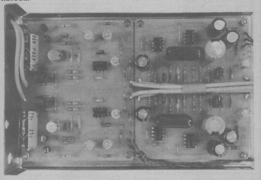
Fig. 3 Component overlay for the moving magnet stage.
---------
PARTS LIST
MOVING-MAGNET STAGE
Resistors (all 1/4W metal film, 5% unless stated otherwise)
R1,101 47k R2,102 470k R3,103 120R R4,104 1k0 R5,105 4k71% R6,106 270R 1% R7,107 6k8 1% R8,108 1k21% R9,109 470R 1% R10,110 47k 1% R11,111 5k6 1% R12,112 IMO R13,14, 113,114 47R
Capacitors
C1,101 C2,102 C3,103 C4,104 C5,105 C6,106 C7,107 C8,9,108,109 270p ceramic
100u 16 V PCB electrolytic 22n polyester 1u0 polyester 220u 16 V PCB electrolytic 56n polyester 33u 25 V PCB electrolytic 100u 25 V PCB electrolytic
Semiconductors
IC1,2,101,102 NE553-IAN
Miscellanies:
PCB (see Buylines); assorted mounting hardware; shielded cable.
--------------------------

Fig. 4 Circuit of one channel of the moving coil input stage. Components
for the other channel are designated R101, C101, IC101, etc.
-----------
HOW IT WORKS
MOVING-COIL PREAMP
The input from a moving coil cartridge is fed via L1 and capacitors C3 and C4 to the base of one of the transistors in the LM394, which functions as a differential input stage.
Q1 and Q2 form a constant current source, which stabilizes the DC operating point and ensures a high impedance source to the emitters of the differential pair. The constant current source works by ensuring that a constant voltage is maintained across a fixed value of resistance. Resistor R3 is used for this purpose, with the base emitter voltage of Q2 expressed across it. If the current through R3 were to try to increase even slightly, the voltage on the base of Q2 would be increased, turning Q2 on harder.
This causes the voltage on the collector of Q2 to decrease, decreasing the current through R3. So Q2 provides negative feed back acting to correct any deviations in the current flowing through the differential pair.
The collectors of the LM394 are shunted by the 1n0 capacitor CS. This decreases the gain of the first stage at high frequencies and helps to ensure stability (ie: freedom from high frequency oscillations).
The input stage is operated in full differential mode by connecting both collectors to inputs of the NE5534AN. If this is not done, the voltage gain of the input stage is decreased and the signal-to-noise ratio is degraded. Because differential pairs have two base-emitter junctions in the input circuit, their total equivalent input noise is inferior to that of a single transistor.
However, since it is possible using a differential pair to obtain noise figures of the same magnitude as the thermal noise of the cartridge, the marginal decrease in the theoretically best signal-to-noise ratio is of little consequence. On the other hand the inherent linearity of a differential pair offers a significant advantage over a single transistor, improving both distortion and high frequency stability.
Capacitor C7 ensures stability of the op-amp by providing adequate compensation for the increased gain around the stage due to the differential pair. C9 provides DC isolation of the stage. The resistors R9 and R10 form a potential divider to decrease the signal level to that suitable for the MM in put. If the particular moving coil cartridge used requires a different amount of voltage gain than is provided, the value of R9 can be changed accordingly. Replacing R9 with a short circuit (ie: a piece of tinned copper wire in place of the resistor on the circuit board) increases the voltage gain of the stage slightly over 100.
The two RC networks, R11, C10 and R12, C11 provide isolation of the supply voltage from other stages using the same power supply. This decreases interactions between stages, thereby improving crosstalk and the overall stability of the preamplifier.
----------
BUYLINES
These low level input stages have been designed to deliver state-of-the-art performance--as we've not compromised on the design we suggest you don't compromise on the components. Both the MM and MC stages use high performance NE5534AN op-amps; a possible alternative to this is the TDA1034 op-amp. Accept no substitutes.
The LM394 and NE5534 are available from Watford Electronics, as is the Neosid balun core; the latter item can also be obtained from Neosid Small Orders, PO Box 86, Welwyn Garden City, Herts A L7 1 AS.
Technomatic stock the LM394 and the TDA1034. The PCBs are essential to preserve the layout and earthing; a very necessary requirement if the full performance is to be achieved. Boards will be available from our PCB Service at the prices listed on page 81.
-----------
Construction
Construction boards is relatively straightforward, since almost all the components are mounted on the PCBs. Resistor R1 and capacitor C1 on the moving magnet board are intended to be mounted directly across the back of the input socket. Order of construction is not critical, although it is probably easier to mount small components first, followed by the larger components such as the electrolytic capacitors, ICs and transistors; these components will be damaged if the unit is powered up with them inserted incorrectly. Shielded cable should be used on all inputs and outputs. We have used mono shielded cable rather than the stereo type for ease of soldering.
The inductor on the input of the MC stage consists of two turns wound on a ferrite balun core, 6 mm long by 13 mm wide. We used the type given in the Parts List.
Each of the PCBs is a stereo input amplifier, with each channel sharing a common input earth track running down the centre of the board. The power supply wiring from each channel on the board can be connected in parallel, so only three wires (+ need to be brought out for power.
The input earth is not connected to the 0 V line from the power supply at any place on the PCBs. This means that without a separate 0 V connection added to the input stage they will not work. This has been done deliberately to ensure that hum present on the earth line, due to supply bypass capacitors for example, cannot modulate the signal earth, producing hum in the output. The 0 V line on the boards is, in fact, a separate supply bypass earth line and is not equivalent to the signal earth. A separate wire should be run from the centre point (0 V point) of the power supply used to signal earth at the input sockets.
Both boards should be mounted in a steel box which can be mounted as a unit inside the main preamp chassis.
This greatly improves the rejection to 50 Hz magnetic fields generated by nearby power transformers or 240 V cables.
---------------
MOVING-MAGNET INPUT STAGE
Gain:
Frequency response:
Total harmonic distortion:
Headroom:
Noise:
S/N ratio: 74, 1 kHz
SPECIFICATION
Conforms to RIAA Equalization
*0.2 dB (This is the performance of the prototype. The actual figure obtained will be determined by the accuracy and long-term stability of the components used.)
<0.001%, 1 kHz, 10 mV RMS input >28 dB with respect to 5 mV RMS input signal ie:135 mV RMS max.
Total equivalent input noise:
112 nV 'A', input shorted, 216 nV flat, input shorted.
1 mV Flat 73 dB A-weighted 78 dB 5 mV 87 dB 92 dB
MOVING-COIL INPUT STAGE
Gain:
Frequency response:
24 7 Hz-135 kHz + 0,-1 dB
Total harmonic distortion: <0.003%, 1kHz, 30 mV input
Noise: Total equivalent input noise:
83 nV flat, input shorted.
42\nV 'A', input shorted 56 nV flat, after RIAA Eq, input shorted 34 nV 'A', after RIAA Eq, input shorted SIN ratio of MC stage after RIAA
Equalization:
10 mV 60 uV 200 uV 500 uV 93 dB Flat 61 dB 71 dB 79 dB 98dB A-weighted 65 dB 75 dB 83 dB
-------------------
RESPONSE Hz
IDEAL RIAA dB
MEASURED dB
2-0.2-0.2 4 +5.7 +5.7 8 +11.2 +11.2 16 +15.4 +15.4 20 +16.3 +16.3 30 +17.0 +17.0 40 +16.8 +16.8 50 +16.3 +16.2 80 +14.2 +14.2 100 +12.9 +12.8 150 +10.3 +10.2 200 +8.2 +8.1 300 +5.5 +5.4 400 + 3.8 +3.7 500 +2.6 +2.6 800 +0.7 +0.7 1k ' 0.0 0.0 1k5-1.4-1.3 2k-2.6-2.4 3k--4.8--4.7 4k-6.6-6.6 5k-8.2-8.1 6k--9.6-9.6 8k-11.9-11.9 10k-13.7-13.8 15k-17.2-17.1 20k-196-195
----------------
PARTS LIST
MOVING-COIL STAGE
Resistors (all 1/4W metal film, 5%) R1,101 220R R2,102 100R R3,103 39R R4,5,104,105 390R R6,106 22k R7,107 6R8 R8,108 680R R9,109 3k3 R10,110 1k0 R11,12, 111,112 270R Capacitors C1,3,101,103 C2,5,102,105 C4,104 C6,106 10n polyester 1n0 polyester 470u 16 V axial electrolytic 680p ceramic C7,107 C8,108 C9,109 C10,11, 110,111 100p ceramic 220p ceramic 10u 16 V PCB electrolytic 47u 25 V PCB electrolytic Semiconductors IC1,101 LM394CH IC2,102 NES534AN Q1,2,101,102 BC549 Miscellaneous L1 Two turns on ferrite balun core, Neosid type 105012IF14 or 42-002-31 PCB (see Buylines); assorted mounting hardware; shielded cable.
--------------------

Fig. 5 Overlay for the moving coil input stage.
Powering Up
No setting-up procedure is required for either stage, but make a final check of all components before applying power to the unit.
= = = =