To generate FM signals, two general methods are in use. One is the reactance method; the other, the phase-shift method. In the reactance method, the frequency of an oscillator is made to vary with modulation through the use of a vacuum tube. In the phase-shift method, frequency modulation is achieved by varying the phase of a signal obtained generally from a crystal oscillator. Sections 14 and 15 describe commercial FM transmitters employing reactance tubes, whereas Section 16 is concerned with transmitters utilizing the phase-shift system.
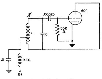
Fig. 14.1. A Hartley oscillator.
Reactance-Tube Circuit. Probably the most direct method of producing a frequency-modulated wave is through the actual variation of one of the frequency-determining components of an ordinary oscillator. Consider the Hartley oscillator shown in Fig. 14.1. In this circuit, the frequency which the oscillator will generate is determined primarily by L and C according to the familiar formula,
I 1
= 2'1n/W
By varying either or both of these components, it is possible to alter the resonant frequency. For the production of a frequency-modulated signal, we would have to have either L or C vary in accordance with the spoken word or a musical selection.
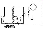
Fig. 14.2. An elementary method of frequency modulating an oscillator.
One crude and elementary method of obtaining a variation in capacitance is by the attachment of a condenser microphone in parallel with the tuning capacitor C. Such an arrangement is shown in Fig. 14.2. As long as no sound reaches the microphone, the total capacitance across the coil remains constant. The frequency due to this combination of L and C would represent the central or resting frequency. C, in this case, is the sum of the average capacitance of the micro phone plus the tuning capacitance.
When the microphone is actuated by sound, the movable capacitor plate is forced to vibrate back and forth about its rest or center position.
At some time, under pressure of the moving air, the capacitor plate approaches the fixed plate and the total capacitance increases. (Capacitance varies inversely with plate spacing.) As a consequence, the frequency of the oscillator decreases. Upon being released from this position, the movable capacitor plate swings past its center position and comes to rest at a point farther away from the fixed plate. Under these circumstances, the total capacitance has decreased below its average value, increasing the oscillator frequency. Thus the frequency of the oscillator varies in step with the impressed audio variations and a frequency-modulated signal is developed. True, the linearity of this converter is not very good, and the results would not be commercially satisfactory. However, it does illustrate the production of a frequency-modulated wave.
The attachment of a capacitor microphone across the tank circuit is impractical, but we can obtain a variation in either inductance or capacitance by means of a vacuum tube. As will be seen, the tube does not actually "add" or "subtract" a capacitor or coil across the tank circuit. However, because of its presence in the circuit, the effect produced is as though a variable inductance or capacitance were actually in the circuit. Consequently, the frequency of the oscillator changes. If the circuit is designed so that the frequency variations are governed directly by the audio sounds reaching the microphone, we have the desired frequency-modulated signal.
Reactive Impedance. Before we actually examine the circuit of a reactance tube, let us review brief0ly the ideas of resistive and reactive impedance. Consider pure resistance first. Any physics book will demonstrate that what is called resistance is merely the ratio of voltage across a conductor to the current flowing through it. We express this by Ohm's Law, R = E/1. If a given voltage produces a high current flow, then we say that the conductor possesses a small resistance or opposition. If a small current is produced, for the same voltage, then we say that the conductor has a high resistance. In any event, the resistance is never measured as such, but solely as the ratio of voltage to current. Recall any resistance measurements or experiments that you have performed or seen performed. Were any of these ever made without the use of voltage and current? The answer is no. In a limited sense, then, we may consider resistance as existing only when current is flowing through the circuit. Without current and voltage, resistance loses its significance.
What has all this to do with reactance-modulator tubes? We shall see in a moment. Now let us turn our attention to inductive and capacitive reactance. We learn early in our study of radio that for many common frequencies the opposition that a resistor offers is constant. But when we insert a capacitor or an inductance into the circuit, we note that the opposition depends upon the frequency of the applied voltage. For the capacitor, the opposition decreases with rise in frequency; for the inductance, it rises directly. Here, then, more so than in the case of the resistor, we see that the concept of opposition cannot be separated from the applied voltage and its ratio to the current flowing in the circuit.
From these few facts we can draw one simple, yet highly important, conclusion. A circuit may appear (to some other circuit, for example) either capacitative, inductive, or resistive depending upon the voltage and current conditions in that circuit and not upon whether capacitance, inductance, or resistance is actually present. In other words, if we take a tube and so connect it that the voltage between its plate and cathode is 90° lagging the plate current, then it will appear as a capacitor to any circuit connected to this tube. Why? Simply because it is the voltage-to-current ratio and their relative phase that are the determining factors and not the mere fact that certain components have been placed in the circuit. Remember these points, for they will greatly simplify the understanding of reactance tubes.
A Reactance-tube Modulator. The fundamental circuit of a reactance tube modulator is shown in Fig. 14.3. Basically, its function is to vary the frequency of the oscillator in step with an applied audio voltage. For the moment, the audio voltage has been omitted. However, as soon as we under stand how a tube can cause the frequency of an oscillator to vary, we will incorporate an audio signal.
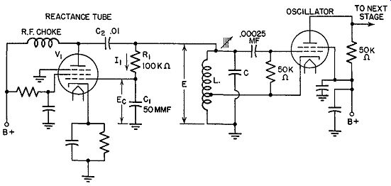
FIG. 14.3. A reactance-tube modulator.
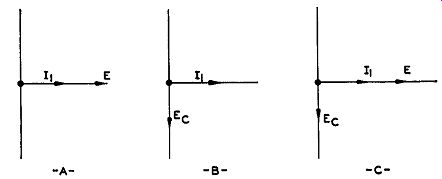
FIG. 14.4. (A) Phase relationship between oscillator tank voltage and
current through R1 and C1 . (B) Current and voltage phase for a capacitor.
(C) The phase of Ee with respect to E and / 1 .
To begin, we note that, since the reactance tube is connected across the tank circuit of the oscillator, any voltage here will also be present across R1 and C1 (see Fig. 14.3). If we make the resistance of R1 much higher than the opposition of C1 (to this voltage E), then the current that flows through the R1C1 branch will be governed by the resistor and be practically in phase with the applied voltage E. Using vectors, we could show this condition as in Fig. 14.4A. Examine the voltage that is developed across capacitor C1. We know that with every capacitor the current and the voltage (across that capacitor) are out of phase (see Fig. 14.4B). In this instance, since the current through the series branch is practically in phase with the total applied voltage E, and, at the capacitor, the current and Ee (the capacitor voltage) are 90° out of phase, we can add Ee to the vector diagram of Fig. 14.4A to obtain the result shown in Fig. 14.40. Ee lags the current and is placed behind it.
Returning to Fig. 14.3, let us investigate the position of Ea in the circuit.
By its attachment between the grid and ground, it constitutes the grid voltage. Hence, whatever phase relationship Ea might have to the rest of the circuit, the same relationship will exist for the grid voltage of V1. And, since the grid voltage directly controls the plate current, we can derive a relationship between Ea, Ev (the grid voltage of Vi) and the plate current.
C2 serves only to prevent the B+ voltage of V1 from being grounded by L. It is a relatively large capacitance and its impedance at the operating frequency is low.
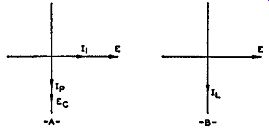
Fig. 14.5. (A) The phase angle between E and IP of V1 . Its resemblance
to the phase relationship between E and / 1, in the oscillator tank
circuit (B) is evident.
Whenever the grid becomes positive, the plate current increases; when ever it goes negative, the current decreases. Both vary directly and both are in phase. Adding the plate current (Ip) to the vector diagram that has been developed already, we obtain the dia gram of Fig. 14.5A. The plate current, being in phase with Ea, is placed 90° be hind voltage E. If we look carefully at this phase relationship between E and Ip, we are immediately aware of one fact. Because of the phase relationship, Ip acts as if it is coming from an inductance. Since Ip comes from the tube, then as far as voltage E is concerned the tube possesses inductance and presents inductive reactance to the outside circuit. Thus, through the peculiar combination of R1C1 and the tube, we are able by a simple procedure to have the plate current of the tube lag the oscillator tank voltage E and appear inductive.
To progress one step further. Voltage E is developed across L and C of the oscillator tank circuit. If we plotted the relationship between the voltage to the current flowing through the inductance of the tank circuit, it would appear as shown by the vectors in Fig. 14.5B. E leads the inductive current of the tank circuit in exactly the same manner as it leads the plate current of V 1. Again the similarity of the tube to an inductance is evident.
Because of the placement of V1 across the oscillator tank circuit, IP must flow through the oscillator coil and add to the inductive current already flowing through the coil L. That it will add is due to the voltage E. This voltage is present across both the tube and the tank coil. Since both inductive currents arise from the same voltage, they will be in phase. The result, due to the presence of the tube, is the same as though another inductance had been placed across the tank circuit. Actually, the tube represents this added inductance, arising from the plate-current phase relationship to the tank voltage. An equivalent circuit is shown in Fig. 14.6.

FIG. 14.6. Equivalent circuit of Fig. 14.3.
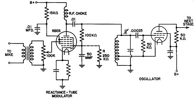
FIG. 14.7. A complete reactance-tube modulator. R may be connected across
the 50-mmf capacitor to provide a d-c path to ground for any stray electrons
trapped on the grid.
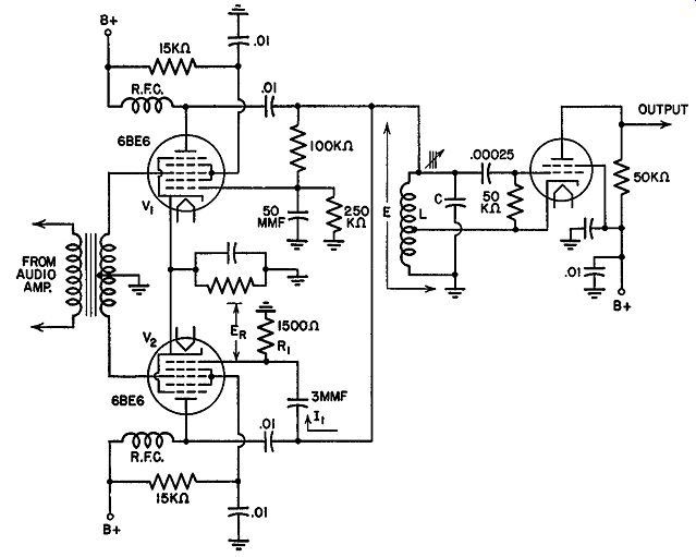
Fig. 14.8. A balanced modulator.
When coils are placed in parallel, their total inductance becomes less than each individual inductance. From the formula for frequency:
1 I= 2 pi y LC
it is evident that decreasing L will produce a higher frequency. Hence, by the addition of a tube across the tank circuit we have succeeded in shifting the oscillator frequency. The new frequency now represents the new resting point of the oscillator. No other change will occur as long as the operating voltages remain steady.
Producing FM. Thus far we have succeeded only in moving the frequency of our oscillator from one point to another. There has been no frequency modulation. This is to be expected since no audio voltages have been applied. This is done in Fig. 14.7, which is essentially the same as the diagram of Fig. 14.3. However, by employing a pentagrid tube we obtain a separate grid (grid 3) for the insertion of the audio voltage. Grid 1 causes the plate current to appear inductive to the oscillator tank voltage E. When no audio voltage is being impressed on the tube, the plate current is steady. Upon the application of an audio voltage, the plate current is varied in step with the voltage. On positive half cycles, grid 3 becomes positive, allowing more electrons to flow. On the negative audio voltages, the plate current decreases below its normal value. The rapidity with which the current rises and falls is entirely governed by the frequency of the audio voltages. People with high-pitched voices will produce faster variations in the 6BE6 plate current than persons having low-pitched voices.
At the oscillator, these variations in plate current (I_p) will have the effect of changing the amount of inductive current flowing through the coil L. We know that the oscillator tank voltage remains constant. Nothing has been done to change it. Therefore, with the voltage constant and a variation appearing in the inductive current of the tank circuit, we can come to only one conclusion. The inductance must be fluctuating. By changing the inductance, we can alter its opposition to the current flow, and this could account satisfactorily for the various inductive currents. A moment's reflection will indicate that a variation in inductance must be followed by a variation in frequency. Consequently, the audio voltages will produce frequency modulation.
In passing, we may note that when the audio voltage is at its positive peak, the maximum inductive current will flow from the tube through coil L. At these moments, the overall or apparent value of L will be smallest (presenting the lowest inductive reactance and hence permitting the largest flow of inductive current). The frequency of the oscillator will be at its highest point. (See previous formula.) During the opposite half of the cycle, when the audio voltage is negative, the frequency is at its lowest point. Remember again that it is the varying effect of the tube across the tank circuit that is responsible for all this. The actual coil and capacitor of the circuit never change.
We have been concerned thus far with a reactance tube that produced a varying inductive current. It is possible to achieve the same results by having the tube appear as a capacitance. This will be done in the next section when a balanced, reactance-tube frequency modulator is investigated.
Balanced Modulators. The degree of frequency shift can be increased and the linearity improved through the use of a balanced modulator, such as illustrated in Fig. 14.8. Two tubes act as reactance units, their grids connected across opposite ends of the audio-signal transformer, whereas their plates are attached to one common point. The purpose of this arrangement is to produce opposite effects in the tubes which will aid each other.
Let us see how this is accomplished.
One tube, V1 , is connected as in the previous circuit. From this we know that the plate current produced by the tube will lag the tank voltage E and appear inductive. For V2 , however, we find a slightly different arrangement. We still have a capacitor (3 mmf) in series with a resistor, but their impedance values are reversed. The capacitance, because of its very small capacitance, presents a much greater opposition to the flow of current through this branch than the 1500-ohm resistor. Hence, the current will be almost entirely capacitative and will lead the applied voltage E by practically 90°. This is shown vectorially in Fig. 14.9A. The voltage that is developed across R1 is in phase with the current because, in all resistors, current and voltage are in phase. We may add ER to the vector diagram, as in Fig. 14.9B. Since the grid obtains its input voltage from the resistor, we see that Eu and ER are one and the same thing. In the vector diagram of Fig. 14.9B we can place Eu at the same point as ER. Proceeding with the analysis, we note that Ip of V 2, being governed directly by Eu, is also in phase with it. Hence, we arrive at a situation where, for V 2, the plate current is 90° ahead of the applied oscillator voltage E (see Fig. 14.9C). Thus, by rearranging the capacitor-and-resistor combination and altering their relative values we obtain a plate current that leads instead of lags the voltage E. Thus, V 2 appears capacitative.
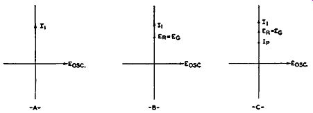
Fig. 14.9. The current and voltage phase relationship in the grid network
of V2 (Fig. 14.8).
Within the tank circuit, this capacitative current combines in phase with the capacitative current flowing through the tuning capacitor C. Whether the effective capacitative effect across the entire circuit increases or decreases depends upon the variations in the plate current coming from V2. If the capacitative current increases, this would have the same effect as a decrease in capacitative reactance. The reason is simple. The tank voltage E remains constant. Hence, the only way the current through C (or L) can change is through a change in the reactance in that branch. For an increase in capacitative current, we must have a corresponding decrease in capacitative reactance. In terms of capacitance this means a larger capacitor because
1 Xe= 2wJC
If Xe goes down, C must increase. The opposite current variation would mean a decrease in C.
Now let us apply an audio voltage to this reactance-tube modulator and determine how the frequency changes.
The grids of the 6BE6's are connected across opposite ends of the audio input transformer. When one grid goes positive, the other grid is driven negative. Suppose that the audio voltage applied to V1 is positive, and that to V2 is negative. Then the plate current lp1 will increase and lp2 will decrease. Across the oscillator tank circuit this will appear as an increased inductive current and a decreased capacitative current. We have seen that an increasing I_p1 means a lower effective inductance across the tank circuit.
We have also determined that a decreasing capacitative current has the apparent effect of a decrease in C. Hence, as a result of the application of the audio voltage, both the effective values of L and C have decreased. From
f = ½ pi __/LC
... we note that the frequency rises. But since both L and C are effected, the overall frequency change is much greater than we could have obtained with the single-tube arrangement of Fig. 14.7.
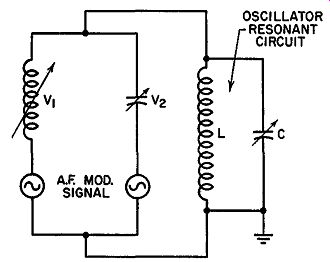
FIG. 14.10. An approximately equivalent circuit of the balanced modulator
of Fig. 14.8. V1 is represented by a variable inductance while V2 by
a variable capacitance.
We could go through the same analysis for the opposite situation when the audio input voltage re versed. However, from what has already been given there is no need for this. The frequency variation is now in the opposite direction, toward the lower frequencies. between the positive and negative audio voltage peaks, intermediate frequency shifts take place at each point directly proportional to the amplitude of the applied voltage.
An approximately equivalent circuit of the balanced modulator of Fig. 14.8 is shown in Fig. 14.10.
The Complete Transmitter. Our progress, to this point, in the forming of an FM signal has consisted solely in examining the action in a reactance tube and the associated oscillator. In practice, the oscillator frequency is somewhere in the neighborhood of 5 mhz. Through the application of an audio signal to the reactance tube, we can vary the oscillator frequency about 4 khz. The output, then, from the oscillator will be 5 mhz ± 4 khz. It is not practical to attempt to obtain a greater frequency deviation because of the non-linearity that rises. Hence, if we desire to reach the ±75 khz authorized by the F.C.C., frequency multiplication must be achieved in the stages that follow the oscillator.
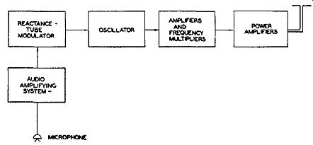
Fig. 14.11. The block diagram of an FM transmitter using a reactance-tube
modulator.
A block diagram of a complete reactance-tube FM transmitter is shown in Fig. 14.11. We are already familiar with the reactance tube and the oscillator. Frequency multipliers are needed to develop the final, signal frequency variation ±75 khz. The power amplifier, of course, is used to raise the signal level to the rated power of the unit, be it 5 kw, 10 kw or even 50 kw. Note that until we reach the power amplifier stages we have relatively low power stages. This permits the use of small, inexpensive receiving-type tubes, with a substantial saving in cost. In AM transmitters, the modulation occurs at or near the final power amplifier. This necessitates large modulating voltages, with their attendant high-power tubes. The cost of such an arrangement is usually considerable.
A second addition to each reactance-tube transmitter is a frequency centering system. The fundamental frequency that is received from the oscillator is the result of the normal resonant frequency of the oscillator tank circuit plus or minus whatever effect the reactance tube may cause by virtue of its attachment across the oscillator. It is well to keep in mind that the simple attachment of the reactance tube ( even when no audio signal is present) produces a frequency shift in the oscillator. Of course, the change is fixed, not varying as when the audio is active. As an example, the oscillator may have a frequency of 4.995 mhz. By attaching the reactance tube, we may raise the frequency to 5.000 mhz. This now represents the normal oscillator output frequency and it is around this value that the audio signal will swing the frequency.
Once the normal or center oscillator frequency has been established, it is extremely important that it remain fixed. Every station is assigned to one frequency and thereafter it becomes their responsibility to maintain the center or normal frequency at this point. Failure to do so will not only ...
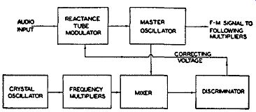
Fig. 14.12. A block diagram of a discriminator control system which
keeps the master oscillator at its assigned center frequency.
... cause interference to stations on other bands, but undoubtedly result in revocation of their operating license by the F.C.C. A simple method that has been successfully used to keep an oscillator on frequency is the system shown in Fig. 14.12. This network is arranged to produce an output voltage from the discriminator if the oscillator frequency shifts. By applying this voltage to the reactance tube, we can vary its plate current and, through this, its effect on the oscillator. If the discriminator voltage is properly applied, it will counteract any tendency on the part of either the oscillator or the reactance tube to change the center transmitter frequency. Note that the correction is applied only to maintain a fixed center frequency. It does not, in any way, interfere with the frequency modulation excursions above and below the resting frequency.
Frequency Multipliers. The output from the modulated oscillator is usually within the frequency range of 4.7 to 6 mhz. The frequency variation, due to the modulation, is generally near 4.2 khz. This is the initial maximum swing, destined to become ±75 khz at the output of the transmitter. Under present frequency allocations, the output carrier is confined to the range 88 to 108 mhz. Hence, we must increase the relatively low oscillator frequency to some value between 88 and 108 mhz. Suppose, as an illustration, we wish to broadcast on 90 mhz. The most common arrangement is to utilize two triplers and a doubler, thus providing the minimum number of frequency multipliers with the proper amount of frequency multiplication. The total amount, then, by which the oscillator frequency is increased is 18 times.
Since we require a 90-mhz output, we find that an oscillator operating at 5 mhz will do nicely. Again, with an eighteen-fold multiplication, an initial frequency swing of 4.1667 khz must be obtained for the loudest audio signal.
Thus, ±4.167 khz, increased 18 times, gives the maximum ±75 khz permitted by the F.C.C.
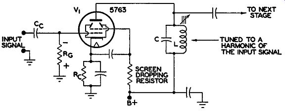
Fig. 14.13. A frequency multiplier. The main grid bias is developed
by Rg; Re is merely for protective bias.
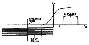
FIG. 14.14. The operating characteristics of a frequency multiplier.
Only the shaded portion of the input signal is effective in producing
plate current.
A frequency multiplier is essentially nothing more than an ordinary amplifier with the output circuit tuned to a harmonic of the input frequency.
In the circuit of Fig. 14.13, the resonant tank, L and C in the output of V1, would be tuned to three times the input frequency. Any voltage that is developed across the tank and transferred to the next stage would be the third harmonic voltage. All other harmonics in the circuit would develop very little voltage across the tank impedance and only a negligible amount would reach the following stage. By successively choosing the desired harmonic, we can raise the original oscillator frequency to any desired value.
Grid-Leak Bias and Distortion. In order to appreciate fully the operation of a frequency multiplier and its function in the FM transmitter, there are several facts we must know. First, in any class C amplifier, such as we find in transmitters, the large grid-leak bias acting at the input of the tube produces a distorted wave in the plate circuit. Grid-leak bias is actually self-bias, where the amount of voltage developed across the grid-leak resistor, Ru, is directly dependent upon the strength of the incoming signal.
Initially, when no input voltage is applied, no bias is present on the grid.
Upon the application of a signal voltage, the grid is driven positive on the positive half cycles and current flows in the grid circuit. The coupling capacitor becomes charged. During the negative portions of the signal the capacitor discharges, tending to maintain a voltage across R_g with the polarity as shown. As long as the strength of the incoming voltage is constant, the bias will keep the tube fixed at one operating point.
The amount of bias voltage developed across R_g will depend upon the size of this resistor (for any one value of input signal). In practice, the resistor is chosen to give a bias equal to approximately 2 or 3 times the cut-off voltage of the tube. If the latter voltage is given as 15 volts by the manufacturer, then the grid-leak bias will be between 30 and 45 volts. Its position is indicated in Fig. 14.14. With this as the operating point, the incoming voltage will vary above and below this value. At the positive peaks, the grid will be driven sufficiently positive to maintain the bias voltage across R_g fixed.
Plate current flows only for that portion of the input voltage when the total grid voltage is more positive than the plate-current cut-off value. This region is shown shaded in Fig. 14.14. The plate current, during those moments when it is permitted to flow, will do so in pulses.
The fact that the plate-current form, produced as a result of the action of the grid bias, is not an exact duplicate of the input signal immediately indicates that distortion has been introduced. It can be demonstrated mathematically that when a wave is distorted, odd and even harmonics of that wave are produced. If the plate tank circuit is tuned to one of these harmonic frequencies, then the major portion of the voltage developed across the coil will be at this harmonic. Transfer to a succeeding stage, also tuned to the same harmonic, will practically eliminate all the other frequencies.
Thus, in Fig. 14.13, tuning L and C to the third harmonic of the input will produce this component across the circuit.
It will be found that multiplication seldom exceeds the third harmonic in any one stage. The reason is simply due to the fact that in any frequency multiplier, the voltage that can be obtained through the use of a harmonic is proportionately lower than if we used the fundamental. For the third harmonic, the output voltage developed across L and C would be usually less than ½ of the fundamental if L and C were tuned to the fundamental frequency. Higher harmonics will give progressively less output.
Although the pulses that are fed into L and C do not resemble sine waves, the fly-wheel action of the tank redevelops them. The pulses keep the current circulating between the capacitor and the coil and this action forms the necessary sine waves at whichever frequency the circuit is tuned.
The plate tank circuit of the frequency multiplier is tuned broadly enough to include any frequency variations of the carrier about its resting point. Thus, if the input frequency to the first tripler is 5 mhz and is accompanied by a ±4.167- khz variation due to audio modulation, it will vary between the limits of 5.004167 mhz and 4.995833 mhz ( 4.167 khz has been changed to 0.004167 mhz and added and subtracted from 5 mhz). At each point in this range, the third harmonic will be produced and developed across the tank circuit. Hence, the output will fluctuate between 15.012501 mhz and 14.987499 mhz. This can be expressed as 15 mhz ± 12.501 khz. Thus we see that both the carrier and the sidebands each receive the same frequency multiplication.
With one more tripler, the foregoing values would be converted to 45 mhz ±37.503 khz. Add a doubler, and we obtain the desired frequency, 90 mhz, with ±75- khz deviation.
After these multipliers, power amplifiers are added in sufficient number until the desired output power is attained.
RCA FM Transmitter. The present RCA FM transmitter incorporates many of the preceding circuits and ideas in its design. It uses a slightly modified pair of push-pull modulators, a Hartley oscillator, two triplers, a buffer amplifier, a doubler, and several power amplifiers. A block diagram is shown in Fig. 14.15.
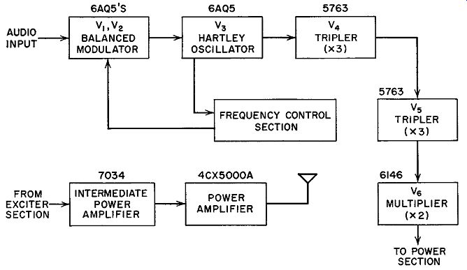
FIG. 14.15. The outline of a modern RCA FM transmitter. The notation
above each block designates the tubes used in that stage.
The balanced modulator differs from the previous balanced modulator in that the grids receive their energy from the oscillator tank circuit by means of a link-coupling arrangement. Previously, it will be remembered, we obtained the R.F. voltage for each grid by means of a resistance-capacitance circuit coupled directly to the oscillator tank. Through this R-C arrangement, each grid received voltages that made them lead or lag the oscillator tank current by 90°. If the plate current of one modulator tube was 90° leading, the current of the other tube was 90° lagging.
In the RCA transmitter, the R.F. voltage from the oscillator is transferred to L1 inductively. (See Fig. 14.16.) The voltage developed across L1 produces a current flow in the link-coupling circuit, establishing a similar voltage across L2 at the other end. The voltage from L2 is then coupled to L3 and L4 inductively.
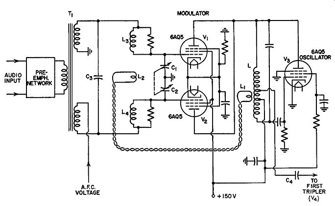
Fig. 14.16. A simplified diagram of the balanced modulator and oscillator
of the RCA FM transmitter.
If we examine the grid circuits of the two modulator tubes, we note that they form essentially a push-pull circuit. The two far ends of L3 and L4 are placed at the same R.F. potential by Cs. Thus we may consider Ls and L4 as being directly connected. C1 and C2 resonate L5 and L4 to the same frequency as the oscillator tank circuit. Since the grids are so connected, each receives R.F. voltages that are 180° out of phase with respect to each other. If one grid is, at one instant, positive, the other grid is negative.
To obtain the required reactance from each modulator, the designers have arranged the link-coupling network, L1 and L2 , in conjunction with the other coils-- L, L3, and L4--so that the R.F. voltage transferred from the oscillator is shifted 90°. Thus, the voltage is first shifted 90° and then applied to L3 and L4 to make each grid 180° out of phase with the other. As a result of this arrangement, each tube presents to the oscillator tank a different form of reactance. However, with no audio input signal at Vi and V 2, the balanced connection of each modulator acts to cancel the reactance produced by each tube at the oscillator tank.
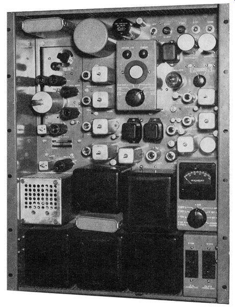
Fig. 14.17. Exciter and driver sections of RCA FM transmitter Model
BTE-10B. (Courtesy RCA).
The audio voltage is applied through transformer T1 to each grid of the modulator. Since the grids are connected to opposite ends of the transformer, the audio voltage will be applied 180° out of phase to each grid. Application of the modulating voltage will upset the balance of V1 and V2 , causing one tube to draw more current and the other tube less current. Across the oscillator tank circuit, the result is the same as if we had varied the reactance (inductive or capacitative), thereby producing a frequency shift. The two tubes, thus, produce a greater frequency shift than if one tube alone had been used in the modulator.
From L, the frequency variations are fed to V 4, the first tripler, by means of capacitative coupling through C4 . The output circuit of V4 is tuned to the third harmonic of the input or oscillator frequency. This, as we have already seen, will triple the input frequency and also the frequency variation, which is the FM. Vis is another tripler, and V6 is a doubler. The layout, to this point, represents the exciter unit and is completely contained within one cabinet (see Fig. 14.17). Included also is a power supply and a frequency control unit.
The center frequency, at the output of the exciter, is somewhere between 88 and 108 mhz. The signal level at this point is on the order of 10 watts.
This is now fed to an intermediate power amplifier where it is raised to 250 watts. Then the signal is applied to a 4CX5000A power tube, and the out- put from this stage is the desired 5 kw. The signal then goes to the FM antenna.
Frequency-Control Circuits. The F.C.C. specifies that each FM broadcast station must be maintained within 2 khz of the assigned center frequency. To insure that this condition is maintained at all times, it has become customary to employ automatic frequency control. This is especially necessary in transmitters that employ reactance-tube modulators because in these units the main oscillator is usually some form of Hartley oscillator.
Unless definite precautions are taken, frequency drift will occur because of the effect of heat, humidity, and aging of tubes and circuit components.
With a properly designed, frequency-correcting network, the carrier will be confined to the regulation limits at all times.
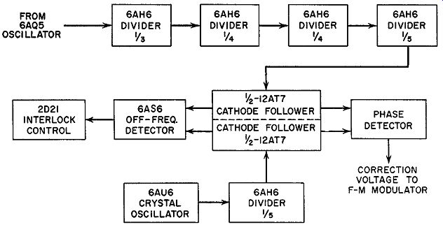
FIG. 14.18. The automatic frequency control section of the FM transmitter
of Fig. 14.14.
The frequency control system which is employed in the RCA FM transmitter of Fig. 14.15 is based upon a comparison of two oscillators-a crystal oscillator and the master frequency-modulated oscillator-to obtain a mean center-frequency control. The frequencies from both units are each divided to a common frequency and then combined in a balanced phase detector.
When the two oscillators are exactly in step, the two inputs to the phase detector are 90° out of phase and the detector output is zero. If the mean frequency of the master oscillator tends to vary from the frequency of the crystal oscillator, the 90° phase relationship is no longer obtained, and the phase detector develops a d-c output which is used as a correction voltage to offset the tendency of the master oscillator to vary. The correction voltage is applied to the control grid of a modulator tube where it directly affects the reactance shunted by this tube across the master oscillator tuning circuit.
A block diagram of the frequency control system is shown in Fig. 14.18.
A portion of the output from the master oscillator is fed to a series of frequency dividers where the input frequency is divided down by a factor of 3 X 4 x 4 X 5, or 240. Since the output from the master oscillator falls somewhere between 4.5 and 6.0 mhz, the output of the frequency divider chain will be 1/240 of these frequencies, or 18.75 khz to 25 khz. (It is under stood that only one center frequency will be obtained from the master oscillator and consequently only one frequency will appear at the end of the divider chain.) At the same time, a crystal oscillator, operating at some frequency between 93.75 khz and 125 khz, has its signal pass through a divider where the initial frequency is lowered by a factor of 5. This will produce a frequency of 18.75 khz and 25 khz, or the same frequency that the master oscillator should produce at the end of its frequency chain if it is exactly on frequency.
The two divided signals are then passed through separate triode cathode followers and applied to the phase detector.
The reason for the extensive frequency division which must be employed stems from the limitations of the phase detector. The crystal oscillator frequency is quite stable in value. However, the instantaneous frequency deviations of the carrier may extend for as much as 75 khz which, in terms of equivalent phase variations, will amount to thousands of degrees. The phase detector, on the other hand, operates over a range of only 180°. Hence, to employ this type of detector, the frequency deviation must be reduced, and this is achieved by the frequency-divider chain. Of course, not only are the frequency deviations reduced, but the carrier frequency as well. In fact, by the time the signal deviations from the master oscillator are reduced by a factor of 240, the instantaneous carrier variation at 100 percent modulation produces a phase variation of approximately 33° when the modulating frequency is 30 cycles.
There is still another reason for using frequency division, and this concerns the varying amplitude of the center-frequency component. It was shown in Section 1 that, when a carrier is frequency-modulated, power for the sidebands is obtained from the carrier. At times, therefore, the carrier amplitude will decrease to zero, making accurate synchronization impossible. The frequency division, however, acts to concentrate the carrier power into a smaller and smaller bandwidth, resulting at the end of the frequency division chain in a signal of substantially constant amplitude ( containing no less than 96 percent of the power of the unmodulated carrier) for synchronization purposes.
Frequency Division. Before we analyze the phase detector, let us examine a frequency divider stage. This is most commonly a combination mixer and oscillator. (See Fig. 14.19.) As an indication of how it functions as a frequency divider, consider the oscillator section first. The oscillator, consisting of L1 and C1 in the plate circuit and L2 in the grid circuit, is tuned to the desired output frequency. L1 and C1 determine the fundamental frequency at which the circuit will oscillate. As is usual in such oscillators, the tube operates on the nonlinear portion of its characteristic curve and the plate current contains many harmonics. Although harmonics are generally not desirable, their presence is required here for the mixing action.
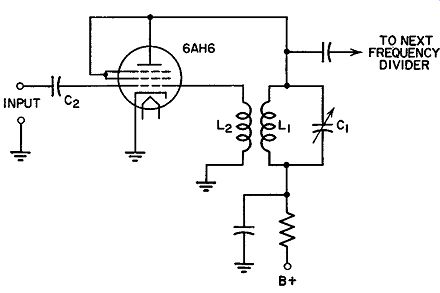
Fig. 14.19. A frequency divider similar to those used in the RCA FM
transmitter.
The frequency to be divided is fed to the oscillator through the capacitor, C2. Let us say that its value is 6.0 mhz. An output one-fourth of this is desired, so that the oscillator functions at 1.5 mhz. At the tube the 6.0 mhz will mix with either the third harmonic (4.5 mhz) or the fifth harmonic (7.5 mhz) of the oscillator to produce a difference frequency of 1.5 mhz. Because of the harmonic relationship between the incoming signal and the oscillator voltage, a lock-in will occur, with the incoming signal acting to keep the oscillator at some sub-harmonic value. If the incoming frequency should shift, then the lock-in will still remain, and the oscillator frequency will be shifted or "dragged along." However, the incoming signal will be able to maintain control only within certain limits. If these are exceeded, the oscillator breaks loose and returns to its natural frequency. However, in this circuit, the frequency shift is seldom so great that the lock-in is broken.
The oscillator circuit is designed to follow the incoming frequency over fairly wide limits.
To recapitulate, the oscillator in the frequency divider is set at a sub harmonic of the correct incoming frequency. Then, one of the harmonics of the oscillator mixes with the incoming signal to produce a difference frequency which is equal to the fundamental oscillator frequency. Because of the harmonic relationship of the incoming signal and the oscillator frequency, the two lock-in. Once locked-in, any small shift in the signal will produce a shift in the oscillator and thus indicate to the following frequency dividers that the main FM oscillator is off the center frequency.
Returning to the block diagram of Fig. 14.18, we see that the system contains four frequency dividers. Multiplying each of the frequency divisions together, we obtain a total of 3 X 4 X 4 X 5 = 240. Thus, if the main oscillator is at a frequency of 6.0 mhz, the output of the final divider is 6.0 mhz /240, or 0.025 mhz, or 25 khz.
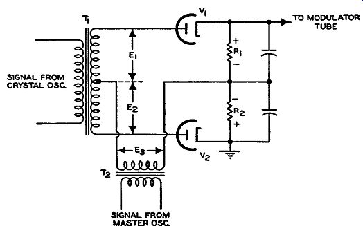
FIG. 14.20. A phase detector.
The overall purpose of the frequency divider is to bring to the phase detector immediate indication of any change in the main oscillator frequency. However, the sole fact that the frequency has shifted is not significant unless it is compared with a standard frequency, one that remains fixed. For this we employ a crystal oscillator. After the output of the crystal oscillator is decreased by one-fifth, its frequency has the same value that the main oscillator frequency should possess after it had been divided 240 times. Hence, if the main oscillator frequency should shift even the slightest amount, this becomes immediately apparent by comparison.
Phase Detector. The phase detector compares the phase between the frequency-divided signals from the master oscillator and the crystal oscillator. When the master oscillator is on frequency, the two signals at the detector will possess a phase difference of 90°. The reason for this particular phase difference is that, under these conditions, the output of the phase detector is zero. The latter condition should occur when the master oscillator center frequency is correct, since at this moment no correction voltage is needed.
To demonstrate that the foregoing conditions exist, consider the circuit of the phase detector shown in Fig. 14.20. The frequency-divided signal from the crystal oscillator is applied to the transformer, T1. Since the secondary is center-tapped, equal voltages appear across each half of the sec ondary winding. These are labeled E1 and E2. Since the voltage polarities at either end of the secondary windings are opposite to each other with respect to the center tap, E1 and E2 can be represented (by vectors) as shown in Fig. 14.21A. E2 differs from E1 and E2 by 90°, as specified above.
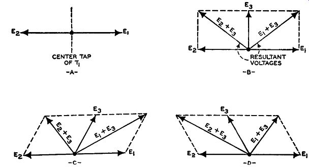
Fig. 14.21. Phase relationships between E1, E2, and E3 of Figure 14.20.
If now, E1 and E3 are added vectorially, and the same is done to E2 and E3, we obtain the resultant vectors or voltages as shown in Fig. 14.21B. E1 + Es is applied to tube V 1, while E2 + Es is applied to V2. Since both resultant vectors are equal in length (i.e., amplitude), the same currents will flow through V1, V2, R1, R2, producing equal voltage drops across the two load resistors. Their combined voltage, which is fed to the control grid of the modulator tube, is zero because of the back-to-back placement of R1 and R2. Consider, now, what happens when the frequency (and, consequently, the phase) of the master oscillator changes from the desired center value. Es will no longer be exactly 90° from E1 and E2. When the master oscillator frequency changes in one direction, Es will approach closer in phase to E1 and hence cause E1 + E3 to be greater than E2 + E3. (See Fig. 14.21C.) V1 will now conduct more strongly than V2 , developing a greater voltage drop across R1 and feeding a positive voltage to the modulator tube. How-ever, when the master oscillator drifts in the other direction, the conditions shown in Fig. 14.21D obtain. Now V2 will conduct more strongly than Vi, giving rise to a greater voltage across R2 and feeding a negative voltage to the modulator. In each instance, the modulator will tend to return the master oscillator to its propercenter frequency.
A 10-cycle low-pass filter is inserted in the path of the correction voltage from phase detector to modulator. Since the lowest modulating frequency used is 30 cycles, the filter removes any residual modulation that may be left.
The only changes that are permitted to reach the modulator are those caused by the drifting of the master oscillator, and these occur at a frequency less than 10 hz.
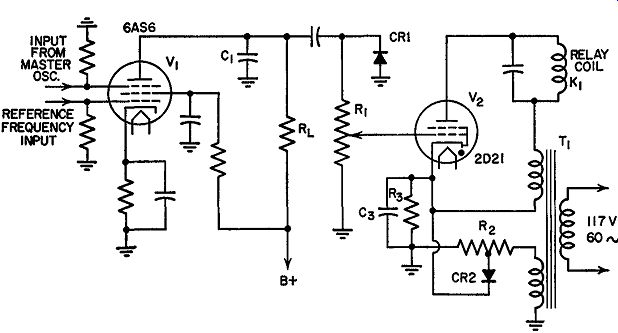
FIG. 14.22. Schematic diagram of the off-frequency detector and interlock
control circuit.
Off-Frequency Detector. In the same A.F.C. circuit, Fig. 14.18, there is a 6AS6 off-frequency detector which also receives the stepped-down master oscillator and crystal oscillator signals. (See Fig. 14.22.) The 6AS6 tube acts as a mixer, receiving each signal at a different grid. When the master oscillator is on frequency, both signals possess the same frequency and zero beat together, producing no a-c output. However, if a difference does appear between the two signals, sum and difference frequencies will be developed.
C1 is designed to offer a low impedance to the sum frequencies, effectively by-passing them away from load resistor, R_L.
The much lower difference frequency does reach RL and is rectified by CR1. A positive d-c voltage will then appear across R1 . If this voltage exceeds the fixed cathode bias applied to the thyratron, V 2 , the tube will conduct and the relay K1 will be energized. This opens up the relay contacts (not shown) and prevents plate power from being applied to stages following the exciter unless the A.F.C. circuit is locked in. Thus, the transmitter is prevented from radiating a signal unless the proper frequency is being generated.
The foregoing automatic frequency control system represents one approach to this problem. Several other methods have been employed and it may be instructive to see how they operate. One interesting system employs a 2-phase motor; another utilizes a discriminator circuit. Both are described below.
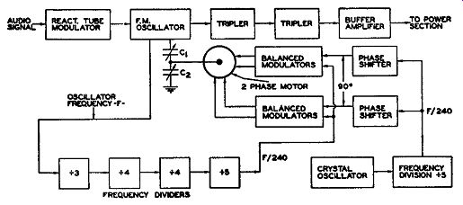
Fig. 14.23. An outline illustrating the several circuits of the frequency
control section.
Motor Control. An outline of an FM transmitter using motor control in the A.F.C. network is shown in Fig. 14.23. Capacitors C1 and C2 , which are mechanically linked to the 2-phase motor, are electrically connected across the master oscillator tuning coil. Any change in the settings of C 1 and C2 will alter the frequency of the oscillator and, with this, the trans mitted carrier frequency. A portion of the oscillator voltage is fed to a series of frequency-divider stages, where a total frequency division of 240 times occurs. Thus, with the main oscillator frequency somewhere between 4.5 and 6.0 mhz, the output of the final frequency divider stage will decrease to the 18.75-25 khz range. (It should be understood that, for any one station, the main oscillator has but one frequency. However, to cover the entire FM band, 88 to 108 mhz, it is necessary to provide the values of 4.5 to 6.0 mhz for the oscillator.) The divider output is then fed to a balanced modulator.
The other input to the modulators is obtained from a highly accurate crystal oscillator. The crystal oscillator frequency is lowered by ½, at which value it will be exactly 1/240th of the correct main oscillator frequency.
This frequency is then compared in the balanced modulator with the frequency obtained from the main oscillator. If any difference exists, the motor is actuated and the tuning capacitors rotated until the oscillator is again centered at its assigned spot.
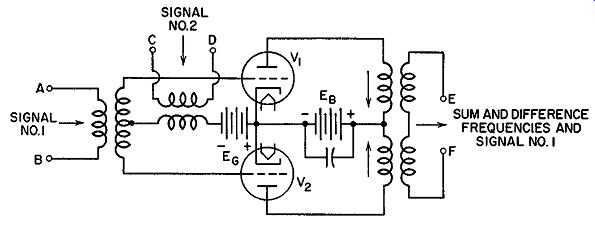
Fig. 14.24. A balanced modulator.
The balanced modulator of Fig. 14.24 differs from the balanced modulator of Fig. 14.8. The latter circuit modulates the frequency of an oscillator, whereas the present modulator mixes two frequencies. Both qualify for the designation of modulator, although their functions differ.
Balanced Modulators. In a balanced modulator we can feed two signals into the grids of the tubes and obtain only one of the input signals plus the sum and difference frequencies of the two signals at the output. The other input frequency does not appear at the output. In the circuit of Fig. 14.24, one signal is applied to terminals A and B, the other signal to terminals C and D, and the sum and difference frequencies appear across points E and F. It is customary to apply the higher frequency at terminals C and D and the lower frequency at A and B. However, in this case, both incoming signals have approximately the same frequency.
The reason the signal at terminals C and D does not appear across E and F is due to its method of application. Both tubes, V1 and V2 , are connected in push-pull, which means that their respective plate currents flow through the output coil or transformer in opposite directions. For V1, the plate current flows down through its winding, whereas for V 2 the flow is up through the coil to the center point. As long as the currents are equal, their opposite effect will cancel.
At the input circuit, any voltage across terminals C and D will be applied to both grids in like measure. The voltage will drive both tubes positive or negative at the same time. Both plate currents will thus be in phase, completely cancelling their magnetic effects in the output.
When we apply another signal at terminals A and B, we upset the equal voltages that the signal at C and D is applying to the grids. When A is positive, B is negative and these voltages, added to those already existing on the grids due to the signal at C and D, produce an unbalance. First, one tube will conduct more current, then the other. The result of this mixing of frequencies in V1 and V 2 is the production of the sum and difference frequencies across terminals E, F. We also find in the output, the frequency of the signal that is applied to terminals A, B. Now let us see how these facts are useful in the FM transmitter. Two balanced modulators are needed, the output of each connected to the windings of the 2-phase motor. The output from the fourth frequency divider (bringing the signal from the main oscillator) is applied to each balanced modulator. We could, for example, feed the signal into terminals, A, B of each modulator. The output of the frequency divider following the crystal oscillator is also fed to each modulator, say terminals C, D. However, there is introduced (through the phase-shift network) a phase difference between the two crystal oscillator voltages of 90°. The need for this is due to the use of a 2-phase motor. In order for the motor to rotate, the two currents flowing in its windings must differ by 90°--hence the phase-shift network.
In the modulators, the two signals mix, producing sum and difference frequencies. Of particular interest in this instance are the difference frequencies. When these currents flow through the two windings of the 2-phase motor, a torque is produced and the motor rotates the attached capacitors.
If both signals have the same frequency, the difference frequency is zero, or d-c. Since the motor requires alternating currents, no torque is produced and no rotation occurs. When signals entering the modulators have identical frequencies, the main oscillator is obviously at the proper operating point.
It may be wondered why the motor does not respond to the sum frequencies, or the frequency of the signal that is applied across terminals A, B. These are also present in the output. Sum frequencies are produced as long as two signals are present, whereas difference frequencies occur only when the two signals differ in frequency. The reason the motor responds only to difference frequencies is due to its operational characteristics. It will not respond to frequencies beyond 1000 cycles. Since either input signal or the sum frequencies (produced through the mixing of the signals) are always above 1000 cycles, they cause no motor rotation.
Discriminator Control. Another interesting method of frequency control relies on the operation of a discriminator. In Fig. 14.12, a block diagram illustrates the essential features of the system. As before, a crystal oscillator is the standard against which the main oscillator frequency is compared. As soon as deviations occur in the oscillator center frequency, an output (d-c) voltage is obtained from the discriminator. If the oscillator frequency drifts to a higher value, the output voltage of the discriminator is of one polarity.
Should the frequency drift below its normal value, then the voltage from the discriminator reverses. The application of the d-c voltage from the discriminator to the control grid of the reactance tube controls the effect of the reactance tube on the main oscillator and, through this, the center frequency.
The corrective voltage applied to the reactance tube is always of such polarity (either positive or negative) as to bring the main oscillator center frequency back to its assigned position.
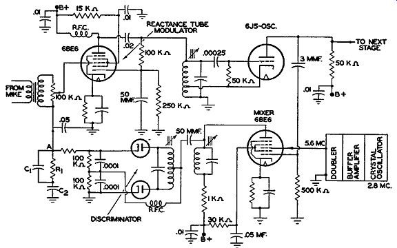
Fig. 14.25. A discriminator frequency-stabilization circuit.
A frequency stabilization circuit is shown in Fig. 14.25. The resonant frequency of the crystal oscillator is at 2.8 mhz. This voltage is passed through a buffer amplifier and then doubled in the frequency multiplier to 5.6 mhz. From the output of the doubler, the 5.6 -mhz voltage is applied to grid 3 of a 6BE6 tube, connected as a mixer.
The 5.0 -mhz oscillator voltage is picked off by means of a small capacitor and brought to grid 1 of the 6BE6. The two signals beat together in the tube, forming sum- and difference-frequency voltages across the plate tank circuit. Of particular interest is the difference frequency, 600 khz, since this is the center resonant point of the following discriminator. So long as this frequency is the difference frequency produced in the mixer, the output voltage from the discriminator is zero. The reason was shown previously in Section 9.
However, when a change occurs in the main oscillator frequency, the mixing will produce some other difference value. Consequently, an output voltage will appear at point A. If the input frequency to the discriminator is above 600 khz, the output voltage will be of one polarity. If it is below, the polarity will be opposite. From point A the voltage is fed to the grid of the reactance tube. At the tube it affects the plate-current flow and, with this, the shift in oscillator frequency caused by the modulator connection.
The drift of an oscillator is seldom a rapid or sudden affair. Rather, the shift is gradual. To produce a large controlling bias voltage from point A, for only small changes in frequency, the bandwidth response of the discriminator is made fairly narrow. As the selectivity of the discriminator tuning circuit becomes sharper, more output voltage is obtained for any given frequency shift. With additional grid bias, the reactance modulator and the entire system become very sensitive to slight frequency changes. Of course, if the main oscillator frequency should suddenly shift by a considerable amount, we would find that a narrow-band discriminator is useless. However, this almost never occurs. There is one precaution that must be observed when using this network.
The signal fed from the oscillator to grid 1 of the mixer contains frequency modulation. If the correcting voltage developed at the output of the discriminator is permitted to follow these frequency variations, all the frequency modulation produced by the audio signal would be nullified. What we desire to prevent are changes in the main oscillator frequency due to uncontrolled causes, such as heat, humidity or aging of the tubes. We do not want to prevent frequency shifting due to applied audio voltages. The oscillator must be kept at its proper resting point, or central frequency. From this position it will swing back and forth under the influence of the audio modulation.
A low-pass filter is used to eliminate all the frequency modulation from the correcting voltage obtained at the output of the discriminator. In Fig. 14.25, this filter consists of C1, R1, and C2. It cuts off at approximately 10 cycles and effectively by-passes or eliminates all audio variations ( caused by the reactance tube in modulating the oscillator) and permits only the very slow frequency drifts of the oscillator to be effective. The center frequency of the oscillator drifts very slowly, well within 10 hz.
EXAM
1. What two general methods are employed to develop FM signals?
2. What is a reactance tube? Does this differ in physical characteristics from any other tube? Explain.
3. Draw the schematic circuit for a simple reactance-tube modulator.
4. Explain the operation of the modulator drawn in Question 3.
5. A simple series circuit containing a resistor and capacitor is connected to an R.F. generator. When will the voltage developed across the resistor be nearly in phase with the applied R.F. voltage? When will this resistor voltage be almost 90° out of phase with the R.F. voltage?
6. To the circuit of a Hartley oscillator add a vacuum tube which appears as a pure resistor to the oscillator tank circuit.
7. Explain what causes a tube to function as a resistor, capacitor, or inductor.
8. How does an applied audio voltage cause the reactance tube to alter the frequency of an oscillator?
9. What are the advantages of a balanced reactance-tube modulator?
10. Explain briefly the difference between balanced and single-ended reactance tube modulators.
11. Is the FM signal fully developed at the output of the modulated oscillator? Explain.
12. The signal obtained from the output of an oscillator had a frequency of 5.6 mhz with an FM swing of 4.0 khz. How could we obtain a carrier frequency of 100.8 mhz? How much frequency swing would we produce in raising the original 5.6 mhz to 100.8 mhz?
13. What precautions can be observed to insure that the frequency of a reactance tube modulated oscillator is kept on-frequency?
14. Explain the operation of a frequency multiplier.
15. Explain briefly the operation of the frequency control employed in the RCA FM transmitter.
16. Explain briefly the operation of the frequency-control circuit in Fig. 14.18. Illustrate by means of a block diagram.
17. How does a phase detector operate? Explain in detail.
18. How does a frequency divider function? What is its purpose in the RCA FM transmitter?
19. Contrast a discriminator frequency control network with a motor-controlled circuit.
20. Draw the block diagram of a discriminator frequency-control network and explain how it functions.
21. Draw the block diagram of a complete FM transmitter containing the following components.
1. Reactance-tube modulator.
2. A 3-stage audio-amplifier system.
3. Two triplers and a doubler.
4. An intermediate power amplifier.
5. A power amplifier.
6. A discriminator type of frequency control circuit.
+++++++++++