Discriminator Action. The heart of the FM receiver, where the frequency variations are reconverted to intelligible sound, is the discriminator.
Since the intelligence is contained in the different instantaneous positions of the carrier frequency, the demodulating or detecting device must be such that its output varies with frequency. This is the bald, overall action of a discriminator. A closer inspection of the present discriminator will disclose that it is a balanced circuit, producing its frequency discriminations by properly combining the outputs of essentially two circuits. Whereas this form of discriminator does not readily indicate its mode of operation, its forerunner does, and we will investigate it first. The circuit is shown in Fig. 9.1.
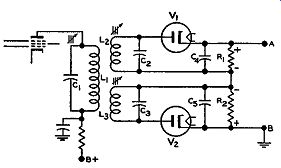
FIG. 9.1. An early form of discriminator.
The secondary contains two separate windings. L1 and C1 form the plate load of the last limiter stage preceding the discriminator. The tuning circuit is broadly tuned to the I.F. center value, broad enough to pass the 200 khz required by a frequency modulated signal. L1, L2, and La are all inductively coupled and the energy contained in L1 C1 is transferred to L2C2 and L3C3. Each of the two secondary circuits is a detector circuit in itself, complete with diode rectifier and load resistor. They are placed end to end, as shown in Fig. 9.1, in order that their output may combine to provide both the negative and the positive half cycles of the audio wave.
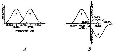
Fig. 9.2. (A) The secondary response curves. (B) The same curves as
in (A) in a position corresponding to the voltage developed across the
load resistor.
To obtain the frequency discriminating action, L2C2 is peaked to a frequency approximately 75 to 100 khz below the center I.F. value, while C3L3 is peaked to a frequency the same number of kilocycles above the I.F. center point. It makes little difference which circuit is above or below, provided both are not peaked to the same point. In Fig. 9.2A, the frequency response curves of both tuned circuits are shown with respect to frequency. In Fig. 9.2B, they have been arranged-as the circuit wiring is arranged-to produce either a negative or positive output. If there is any doubt of this, trace the flow of current through V1 and V 2 and through their respective load resistors, R1 and R2. From the polarities obtained (Fig. 9.1) it can be seen that the polarity of the voltage obtained at the output terminals A and B will depend upon which resistor develops the larger voltage. If the voltage appearing across R1 is larger than the voltage at R2, the output polarity will be positive. If, however, ER2 is greater than ER1 , the output voltage will be negative. Now we can discuss the discriminating action.
Each secondary resonant circuit is tuned to a different peak, and the amplitude of the voltage developed across R1 or R2 will depend upon the frequency of the signal present at that particular instant. For example, suppose that the incoming carrier is at the mid-point frequency, hence containing no modulation. From Fig. 9.2B, the amount of voltage developed across L2C2, at this frequency, is shown by point 1 on its response curve. Assuming no loss of voltage in the tube, this same voltage will be developed across R1, with the top end of the resistor positive. L3C3 will also respond to this frequency, the amount of voltage indicated from the response curve by point 2. This, too, will be the amount of voltage present across R2, but of such a polarity as to oppose E_R1. The output, because of the cancellation of voltages, will be zero. This is as it should be, for with no frequency modulation no output should be obtained.
When modulation is present and the frequency of the carrier begins shifting above and below the center frequency, then a definite output voltage will appear. Suppose, for example, that the carrier frequency shifts to point 3, which is above the normal center frequency. The voltage across L3C3 will be greater than that present across L2C2 because the frequency of the carrier is now close to the resonant peak of L3 and C3. Hence, while some voltage may be present across R1 to cancel part of the voltage at R2, there will still be considerable voltage remaining at R2. This will appear across terminals A and B. As the frequency of the carrier shifts back and forth, at a rate determined by the frequency of the audio note that produced the modulation, the output will rise and fall, through positive and negative values, and the frequency variations will be converted into their corresponding audio variations.
Since the output voltage represents the difference between the potentials present across R1 and R2 , we can combine both response curves into one resultant curve. This has been done in Fig. 9.3.
If properly designed, the response curve will be linear throughout the operating range X to Y and no distortion will be introduced when the FM signal is converted to audio voltages. Should the extent of the linear operating section X-Y be so small that the signal variations extend into the curved sections beyond, then a good reproduction of the audio signal will not be obtained. To guard against this, it is customary in practice to design a discriminator that is linear for a range greater than the required ±75 khz. In most cases, the curve extends to ±100 khz or more. The methods for aligning a discriminator are given in Section 11.
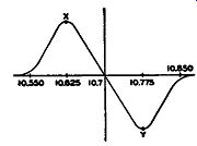
FIG. 9.3. The resultant curve derived by combining both separate curves
of Fig. 9.2B.
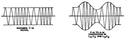
FIG. 9.4. The first step in the process of converting the FM signal
to the final audio voltage.
Capacitors C4 and C5, Fig. 9.1, are for the purpose of by-passing the intermediate frequencies around the load resistors to prevent them from reaching the audio amplifiers. In choosing these capacitors, care must be taken to see that they are not made so large as to by-pass the higher audio frequencies. Usual values range around 0.0001 mf. This is large enough for the I.F., but too small for the highest audio notes. R1 and R2 may be about 100,000 ohms.
In this discriminator, we have essentially two separate actions in converting the FM to audio signals. First, within the tuned circuits, the frequency modulation is changed to the corresponding amplitude modulation.
If we were to picture the waveform change, it would look as shown in Fig. 9.4. As yet, however, we cannot hear any audio signals because the AM wave is at the I.F. values. By inserting an amplitude detector--a diode we reconvert the AM to audio. Thus we change FM to AM and then obtain-with a conventional AM detector--the audio output. It is for this reason that limiters are necessary before the discriminator. Since part of the discriminator relies on amplitude demodulation and since this type of detector is sensitive to amplitude differences, we must use a limiter to present to the discriminator a pure FM signal. Only in this way can we be sure that the AM obtained is completely derived from the FM and not from any extraneous, unwanted signals that may have found their way into the circuit. It will be shown later that with a ratio detector it is possible to reduce the effect of amplitude modulation with less limiting.
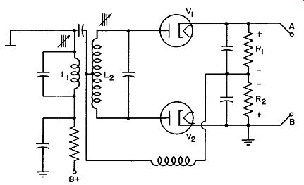
FIG. 9.5. A modified discriminator in widespread use today.
A Modified Discriminator. The foregoing discriminator contains one primary and two secondary capacitors. A more compact unit, one that re quires only two adjustments, is the discriminator shown in Fig. 9.5. Both secondary windings are combined into one coil and a single capacitor is used to bring the secondary to the mid-frequency of the I.F. band. Both primary and secondary circuits are inductively tuned by means of movable cores, in accord with present practice. The discriminator output voltage does not depend now on the different response of two tuned circuits to an incoming frequency; instead, the voltage applied to each diode depends upon the phase of the voltage in the secondary winding as compared to the phase of the primary voltage. In other words, by using a single secondary circuit, we must rely upon phase variations within that circuit to discriminate against different frequencies. In the previous discriminator, each secondary reacted separately to each frequency, their rectified outputs combining to give the audio signal. Now each different frequency alters the phase response of the secondary network and this, in turn, causes each diode to receive a different amount of voltage. As before, the rectified voltage across R1 and R2 gives the proper output.
Fundamentals of Coupled Circuits. Before we examine this circuit in greater detail, let us review some fundamental considerations of resonant circuits and the phase relationships of coupled circuits. In Fig. 9.5 we have two circuits that are inductively coupled. Energy from the left-hand coil is transferred to the right-hand coil through the alternating lines of force that cut across from one coil to the other. The energy in L2 appears as a voltage within the coil and, if a complete path is available, current will flow because of the pressure of the induced voltage. To determine the phase of the current flowing in the circuit with respect to the induced voltage, we must know the frequency of the induced voltage, since a resonant circuit responds differently to each frequency. This, incidentally, is the reason resonant circuits are useful in receiving one station to the exclusion of all others.
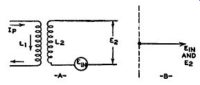
Fig. 9.6. The induced voltage in L2 , due to Ip, is in phase with the
voltage appearing across L2.
When a voltage is induced into a coil, such as in the resonant circuit shown in Fig. 9.5, the current that flows will develop across the coil a voltage that does not necessarily possess the same phase and amplitude as the induced voltage. This is very important and merits additional investigation. Consider, for example, two coils inductively coupled, as shown in Fig. 9.6. Because of the primary current in L1, a voltage appears across L2. If L2 is an open circuit, there is no current flow, and the voltage appearing across L2 is exactly the same voltage--in phase and amplitude--as the induced voltage. If now we connect a resistor across L2, as in Fig. 9.7A, permitting current to flow, then the voltage appearing across L2 will differ from the induced voltage--both in phase and amplitude.
The voltage that is induced in the secondary coil has a complete circuit consisting of the coil and the resistor. The opposition to the flow of current consists of the inductive reactance of L2 and the resistance of R. If R is small in comparison to the inductive reactance, the current flowing in the circuit will be governed almost completely by the inductive reactance and will lag the voltage by slightly less than 90° (this from elementary electrical theory). This is shown graphically by the two vectors, E1 n and I., in Fig. 9.7B.
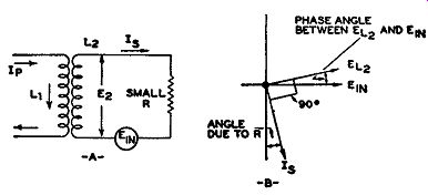
Fig. 9.7. The current and voltage phase relationship in the secondary
circuit.
Now this current, in flowing around the circuit and through L2 will develop a voltage drop across L2 because of the coil's inductive reactance.
As is true for every coil, the voltage will lead the current by 90°. On the vector graph it can be placed in the position marked E1, 2 , 90° ahead of I. Thus we see the extent of the phase difference between E1, 2 and the induced voltage E1 n that produced it.
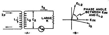
Fig. 9.8. The same circuit as shown in Fig. 9.7 except that R is now
large. Note the difference in the phase angle between E1 n and E12.
The two voltages also differ in amplitude because the voltage drop across the coil plus the voltage drop across the resistor must add up, vectorially, to equal E1n.
Following the same line of reasoning, we get the vector graph of Fig. 9.8 when the inserted resistance is high in comparison to the inductive reactance.
Note that, because of the high resistance, the current flow is more nearly in phase with E1 n, However, no matter how close the voltage, E1 n, and the circuit current approach each other in phase, the voltage drop across the inductance, L2 (or any inductance), is always 90° out of phase with the current through it.
Secondary Resonant Circuit. The next step is to replace the resistor, R, with a capacitor, C2 (see Fig. 9.9). This is now a resonant circuit and the frequency of the induced voltage will determine the phase of the secondary current with respect to the voltage.
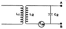
FIG. 9.9. A secondary resonant network.
As far as the induced voltage is concerned, the coil and capacitor form a series circuit.
But if we consider the output terminals of the circuit, points A and B, then we have a parallel circuit. At the moment only the current within the circuit is of interest. Hence, we shall regard this as a series-resonance circuit.
The impedance offered to the circulating current will depend upon the frequency of the induced voltage. If the resonant frequency of the circuit is the same as the frequency of the in coming signal, a large current will be obtained. At the resonant frequency, the series impedance of the circuit is low because the inductive and capacitative reactances completely cancel each other.
Above and below resonance, the reactances no longer cancel, and the resultant of the two, together with any coil and wiring resistance, presents a greater opposition to the current.
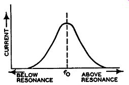
FIG. 9.10. The variation in current in a series resonant circuit.
The nature of the current flow-for any one given induced voltage-is shown by the familiar curve of Fig. 9.10. At the resonant frequency, f0 , the opposition is least and the current largest.
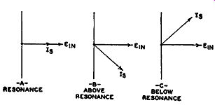
FIG. 9.11. The phase displacements between the induced voltage and
the secondary current for different signal frequencies.
On either side of the resonant point the current decreases be cause the circuit impedance increases.
Fig. 9.10 shows only the variation in current amplitude with frequency. Now let us determine how the phase angle between the current (I,,) and the induced voltage (E1 n) varies, as the frequency changes. At resonance, the sole opposition to the current arises from the incidental resistance in the circuit. Hence, with pure resistance alone, I. and E1 n are in phase. Vectorially, this is shown in Fig. 9.11A. At frequencies above resonance, the opposition of the coil increases, because inductive reactance (XL) is equal to 2 pi f L. Capacitative reactance, on the other hand, decreases with frequency according to the relation ½ pi fC. Hence, above resonance, the XL predominates and the current will lag E1 n. This is illustrated by Fig. 9.11B. Below resonance, the opposite occurs, and the current leads E in.
See Fig. 9.11C. The foregoing phase shifting with frequency is the basis of operation of the discriminator shown in Fig. 9.5. By properly utilizing these phase variations, we can convert FM to audio, obtaining the same results as we did in the previous discriminator.
Discriminator Development. In order to utilize these phase shifts within the secondary resonant circuit, it is first necessary to establish a reference level. At this reference level, which is the mid I.F., no output should appear across the output terminals A and B. This is the same now as it was before, namely, no output with an unmodulated carrier. On either side of the reference point we must unbalance the voltages applied to V1 and V 2 in order that a resultant voltage will appear across A and B. Above resonance, for example, we might have R1 develop the greater voltage; below resonance, ER2 would predominate. In this manner, swinging above and below the center frequency, we obtain positive and negative output audio voltages.
A simple resonant circuit, by itself, is unable to provide the balanced differential output we desire. Fig. 9.12. Development of the modern discriminator. The inclusion of a center tapped secondary and two separate rectifiers produce a balanced network.
Hence, some modifications must be made.
First, by center-tapping the secondary coil and connecting a diode to each end, as shown in Fig. 9.12, we can obtain a balanced arrangement. This will permit a balancing of one tube against the other to give zero output at mid frequency. The circuit, however, is still incomplete because there is nothing to unbalance the voltages applied to V1 and V2 above and below the center frequency. In the present circuit, V1 and V2 will have at all frequencies exactly the same applied voltage because L2 is center-tapped and each tube receives exactly half of any voltage developed across L2. As a result, the rectified voltages across R1 and R2 will be equal, and, because of their back to-back placement, opposite in polarity. No resultant will ever appear at terminals A and B. To produce the proper unbalance, C3 and L4 are added, as shown in Fig. 9.13. If we compare this arrangement with the discriminator circuit of Fig. 9.5, we note they are identical.
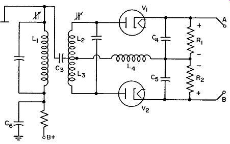
Fig. 9.13. The complete discriminator. This is known also as a Foster-Seeley
discriminator.
Discriminator Operation. The circuit of V1 includes L2 , which is half of the secondary coil, choke L4 , C4, and R1. The other half of the balanced secondary includes V2, L3, L4, C5, and R2. Note that L4 is common to both V1 and V 2 and is introduced to provide the reference voltage in order that an unbalance will occur at frequencies above and below the mid-frequency.
One end of L4 attaches to the top of L1 through C 3 whereas the other end reaches ground through C5 or, what is the same thing, the bottom of L1. L4 then is in parallel with L1. C3, C5, and C6, which aid in placing the choke L4 across L1, have negligible opposition at the high I.F. values. Hence, all of ELi appears across L4. Thus, the reference voltage for the discriminator is the voltage across the primary coil, L1. More on this in a moment.
The secondary coil is divided into two equal sections, L2 and L3. When ever current flows through the coil, we know that one end becomes positive with respect to the other end. The tap, being in between both ends, will be negative with respect to the positive end and positive with respect to the negative end. We could, if we wished, arbitrarily call this point zero. Both secondary circuits connect to the center terminal, and we can indicate the polarity of the voltage applied to each tube with respect to this center terminal. This is shown in Fig. 9.14. The arrow pointing up is the positive voltage, E2 ; the arrow pointing down is the negative voltage, E3. Both are taken with respect to the center tap. Now let us add L4 with its voltage. We shall assume that a mid-frequency signal is being received. Hence, the current that flows through the secondary resonant circuit is in phase with the induced voltage. Later we shall extend this to include all conditions.
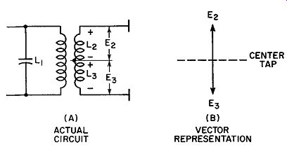
Fig. 9.14. Effect of center-tapping the secondary coil in the discriminator.
Fig. 9.15. (A) The regions of least and greatest change in an a-c wave.
(B) The phase relationship between primary current and induced secondary
voltage.
The incoming signal causes a current to flow through L1 , the primary coil. The magnetic flux, due to the primary current, extends to the secondary winding and gives rise to the induced voltage, E1 n. The greatest voltage is induced in the secondary when the primary flux is changing most rapidly.
The flux changes most rapidly when the current does. In an a-c wave, this change occurs when the current is passing through zero, going from one polarity to another (see Fig. 9.15A). However, the induced voltage is zero when the primary current is not changing, or at those times when the primary current has just reached the peak positive or negative points. If we plot these facts, we see that the current and induced voltage differ by 90°, with the current leading. This is shown in Fig. 9.15B. The voltage, E1, developed across L1 will always be 90° ahead of the current through L1. This, of course, is true of any inductance. If we put E1 on a vector plot, as in Fig. 9.16A, then it must be placed 90° ahead of 11, the current through L1. E1 n, on the same vector graph, must be placed 90° behind 11 as determined above. Hence, we see that the primary voltage and the induced secondary voltage differ by 180°. This is true at all frequencies. Remember that we are discussing E1 and the induced secondary voltage. We have not, as yet, mentioned the voltage across the secondary coil. Most radio men are no doubt familiar with the results which we have just evolved. But, for the sake of clarity, this was methodically determined in order to show how these principles are used in the discriminator.
We can replace E1 by EL4 because, as has been already shown, E1, 4 is in parallel with E1 and is the same voltage. Also, we can drop the primary current vector, it having already served its purpose. The result is merely E1 n and E r, 4, shown in Fig. 9.16B. To the vectorial diagram, we must still add E2 and Es and then combine them with Er, 4
Fig. 9.13 shows quite definitely that the voltage acting at V1, for example, is the combination of EL4 and E2. Likewise, the voltage at V2 is Er, 4 and Es, From their relative magnitudes we can determine which will predominate, and this will indicate the output voltage.
To cover fully the operation of the discriminator, frequencies above, below, and at the mid-point value must be considered. The first illustration will cover the operation with mid-frequency signals. This represents the case of no modulation. Secondly, we will use a frequency above the center point; lastly, a frequency below. Thus, the entire range of an FM signal will be covered. The output voltage from the discriminator will give the circuit response to input frequency variations.
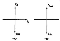
Fig. 9.16. (A) The phase differences between Ei, E1 n and / 1 . (B)
E1 replaced by its equivalent EJA,
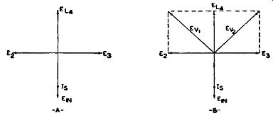
Fig. 9.17. (A) Vector diagram for an unmodulated signal. (B) The vector
addition of E2 with Eu and E3 with Eu,
When the incoming frequency is at the I.F. mid-point, the induced voltage, E1 n, produces a current in the secondary circuit which is in phase with E1 n, At the resonant frequency, the impedance presented to any voltage is purely resistive. Hence, current and voltage are in phase. On the vector diagram, Fig. 9.17A, we can indicate the in-phase condition by drawing E1n and 1. (I,, the secondary current) along the same line. The length of each vector differs because of the resistance in the circuit.
The voltage developed in L2 and Ls, because of 1., differs in phase from 1, by 90°. Again, this condition is true of any inductance. On the vector diagram, we can insert E2 and Es, the voltages developed across L2 and La, both 90° from 18 . E2 and E3 are on opposite sides of 1., because of the center tap on the secondary coil (see Fig. 9.14). E2 and Ea, taken with reference to the center tap, are 180° out of phase with each other. To show this graphically, in Fig. 9.17 A, they are placed pointing in opposite directions.
We can now combine E2 and Er, 4 to arrive at Ev11 the effective voltage applied to tube V1. Also E3 and Er, 4 to derive Ev 2, the voltage applied to V2 . It is evident from Fig. 9.17B that Ev1 and Ev2 are both of equal amplitude. Hence, the same current will flow through each tube and the same voltage will appear across R1 and R2. Since the voltages across these two resistors are in opposition, no output will be obtained. For an FM signal containing no modulation, no output is derived.
Conditions with Higher Input Frequency. Consider next the circuit conditions when the modulated FM signal swings to a higher frequency. At any frequency, the voltage induced in the secondary of the discriminator will be 180° out of phase with the voltage across the primary. Hence, to start the vector diagram, we can insert these two voltages (see Fig. 9.18A). Again, for E1 we can substitute EL4 , and thus far the conditions are the same as for the previous case.
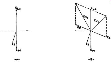
Fig. 9.18. Circuit phase conditions when the signal frequency is above
the I.F. center value,
A voltage having a frequency higher than the resonant frequency of the secondary circuit will encounter more opposition than a voltage at the resonant frequency. Also, because this is a series-resonant circuit (at least, as far as the induced voltage is concerned), the higher frequency will meet more opposition from the coil than the capacitor. Hence, in the present instance, the coil will cause the current to lag behind E1n (see Fig. 9.18A). Now we can draw in E2 and Es, since they differ from the current ( I.) by 90°. I. is responsible for E2 and E3 appearing across the secondary coil, and there is always a 90° phase difference between voltage and current in a coil.
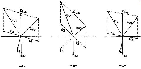
Fig. 9.19. Several additional off-frequency conditions. The input frequency
is high.
Adding E2 and EL4 , Es and EL4 , vectorially, we see that the resultant vectors are no longer equal. In this case, E ., 1 is greater than Ev 2. Consequently, R1 will develop a larger voltage than R2 , and the output voltage will be positive with respect to ground. The amount by which / 8 will differ in phase from E10 depends upon the incoming frequency. The farther this frequency is from the mid-frequency or resonant point of the secondary circuit, the more 18 and E10 will differ in phase. As the position of I, changes, the positions of E2 and E3 will likewise change. Several off-frequency conditions are shown in Fig. 9.19, illustrating the phase shifting that occurs.
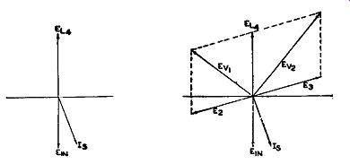
Fig. 9.20. The shift in vectors when the signal is below the I.F. midpoint.
Input Frequency Below Mid-Frequency. The phase analysis when the frequency swings below the mid-frequency value is just as readily accomplished. We can draw in immediately the vectors E10 and EL 4. I_8 follows next. Its position is ahead of E10 because, as the frequency drops below resonance, the capacitative reactance of the capacitor becomes greater than the impedance of the coil. In a capacitative circuit, current leads voltage.
This places I. ahead of E1 n, E2 and Ea are 90° out of phase from I_8, and these can be added to the vector diagram. Addition with E1, 4 shows the un balance of voltages, this time favoring V2 (see Fig. 9.20). The output voltage from the discriminator now becomes negative.
As a summary of the overall picture, the following points are evident:
1. At the resonant frequency, which is the mid-frequency of the carrier, no output is obtained from the discriminator.
2. At frequencies off resonance, an unbalance is created in the circuit, and an output voltage is obtained.
The unbalance that arises from the shifting frequency is made linear with respect to frequency in order that the audio output will be a faithful reproduction of the modulation as effected at the transmitter. The same discriminator S-shaped curve derived for the previous discriminator (Fig. 9.3) is obtained again. The linear section of the curve X-Y generally extends for 200 khz, although the frequency shifts are restricted to a maximum of 75 khz on either side of the carrier. The extension is added protection to insure faithful reproduction.
Other Discriminators. Although the preceding discriminator is widely used, slight variations have been introduced by certain manufacturers. A modified discriminator employed in many sets is shown in Fig. 9.21. The B+
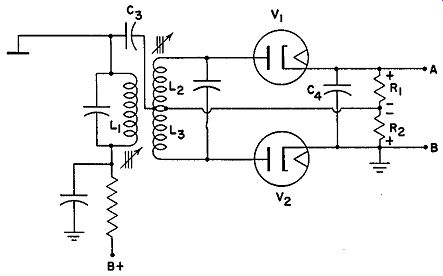
Fig. 9.21. A modified discriminator.
difference between this unit and the preceding circuit is to be found in the elimination of L4 and the use of only one capacitor across the output instead of two. It may appear that Er, 4 , the reference voltage so necessary for the proper operation of the discriminator in Fig. 9.13, has been eliminated. Actually this is not so. The reference voltage is still present, but in a slightly altered position.
If we trace the circuit from the top of L1 through Cs and R2 to ground, we see that R2 is in parallel with L1 and hence E1 appears across R2. If we travel around the network containing V2 , we find that both Es and E1 (from across R2 ) act on V2. This is identical with the preceding case, except that the E1 voltage was obtained from choke L4. Now we have eliminated L4 and placed E1 , the reference voltage, across R2. Thus, in this circuit, R2 performs double duty. Not only does it develop the rectified voltage for V2, but it also serves to apply E1 to V2.
In the V1 network, R1 is also found to be in parallel with L1. The circuit extends from the top of L1 through Cs to R1 , to the top of R1 , then through C4 to ground. Both Cs and C4 offer slight opposition to any high I.F. Thus, R1 is substantially in parallel with L1 . Hence, R1 is to V1 what R2 is to V2 No unwanted intermediate frequencies reach the following audio stages be cause of C4. Its low reactance to intermediate frequencies by-passes them from point A. However, being only 0.0001 mf or so, it does not provide an easy path for the rectified audio frequencies, and these reach the audio amplifiers. Aside from these changes, the operation of this circuit is identical with the preceding network.
The advantage of the circuit lies only in the fewer parts required. R1 and R2 must be kept as high as possible because they are in parallel across L1.
A low value would decrease the impedance of L1 with a subsequent decrease in gain. With the choke, R1 and R2 are isolated from L1, and their effect is not as marked. As a general rule, R1 and R2 may be higher in value in the unit of Fig. 9.21 than that of Fig. 9.13.
The circuit diagram of Fig. 9.21 may be drawn in many ways, one variation being shown in Fig. 9.22. At first glance there appears to be no relationship between the two circuits. On tracing out the wiring, however, it becomes evident that exactly the same discriminator is used. Each manufacturing firm draws schematics along its own peculiar lines and sometimes it requires a little patience to recognize the similarity of identical units.
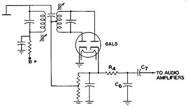
Fig. 9.22. The same discriminator as shown in Fig. 9.21, but slightly
rearranged.
C6 and R4 of Fig. 9.22 form a de-emphasis network to return the signal to its correct values. It will be recalled that pre-accentuation or pre-emphasis is used at the transmitter in order to raise the relative intensity of the higher audio frequencies in an attempt to better the signal-to-noise ratio.
At the receiver the reverse action must be instituted to bring the signal back to its properform. C7 is a coupling condenser.
FM Ratio Detector. The inherent limitations of the preceding discriminators necessitated a limiter stage. The limiter removed all traces of amplitude modulation and presented a pure FM wave to the discriminator. The disadvantage of employing a limiter is the excessive amplification that must be given to the signal before it reaches the limiter. This is necessary in order that the weakest desired signal be brought up to the point where it will drive the limiter to saturation.
If a detector could be built which would develop an output that was in dependent of amplitude variations in the incoming signal, then a great simplification in circuit design could be affected. It would mean that per haps one, at most two, I.F. stages would be needed. Recently, the ratio detector was developed which does not respond as readily to amplitude variations as the Foster-Seeley circuit itself, without a limiter.
To see why a ratio detector is more immune to amplitude variations in the incoming signal, let us compare its operation with that of the Foster Seeley discriminator.
In the discriminator circuit of Fig. 9.13, let the signal coming in develop equal voltages across R1 and R2. This would occur, of course, when the in coming signal is at the center I.F. value. Suppose that each voltage across R1 and R2 is 4 volts. When modulation is applied, the voltage across each resistor changes, resulting in a net output voltage. Say that the voltage across R1 increases to 6 volts and the voltage across R2 decreases to 2 volts.
The output voltage would then be equal to the difference between these two values, or 4 volts.
However, let us increase the strength of our carrier until we have 8 volts, each, across R1 and R2, at mid-frequency. With the same frequency shift as above, but with this stronger carrier, the voltage across R1 would rise to 12 volts and that across R2 decrease to 4 volts. Their difference, or 8 volts, would now be obtained at the output of the discriminator in place of the previous 4 volts. Thus, the discriminator responds to both FM and AM. It is for this reason that limiters are used. The limiter clips off all amplitude modulation from the incoming signal, and an FM signal of constant amplitude is applied to the discriminator.
When unmodulated, the carrier produced equal voltages across R1 and R2. Let us call these voltages E1 and E2, respectively. With the weaker carrier, on modulation, the ratio of E1 to E2 was 3 to 1 since E1 became 6 volts and E2 dropped to 2 volts. With the stronger carrier, on modulation, E1 became 12 volts and E2 dropped to 4 volts. The ratio was again 3 to 1, the same as with the previous weaker carrier. Thus, whereas the difference of voltage varied in each case, the ratio remained fixed. This demonstrates, in a very elementary manner, why a ratio detector could be unresponsive to carrier changes.
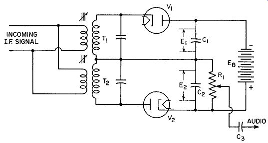
Fig. 9.23. Preliminary form of the ratio detector.
An elementary circuit of a ratio detector is shown in Fig. 9.23. In this form the detector is similar to the detector of Fig. 9.1 where each tube has a completely separate resonant circuit. One circuit is peaked slightly above the center I.F. value (say T1 ); the other is peaked to a frequency below the center I.F. value (say T2 ). The output voltage for V 1 will appear across C1, and the output voltage for V2 will be present across C2. The battery, Eb, represents a fixed voltage. Since C1 and C2 arc in series directly across the battery, the sum of their voltages must equal Eb. Also, due to the manner in which the battery is connected to V1 and V 2 , no current can flow around the circuit until a signal is applied. Xow, although E1E2 can never exceed Eb, E1 does not have to equal E2. In other words, the ratio of E1 to E2 may vary. The output voltage is obtained from a variable resistor connected across C2.
When the incoming signal is at the I.F. center point, E1 and E2 will be equal. This is similar to the situation in the previous discriminators, especially Fig. 9.1. However, when the incoming signal rises in frequency, it approaches the resonant point of T1 , and the voltage across C1 likewise rises. For the same frequency the response of T2 produces a lower voltage.
As a consequence, the voltage across C2 decreases. However, E1 + E2 is still equal to Eb· In other words, a change in frequency does not alter the total voltage but merely the ratio of E1 to E2. When the signal frequency drops below the I.F. center point, E2 exceeds E1. Again, however, E1 + E2 equals Eb. The audio variations are obtained from the change of voltage across C2. Capacitor C3 prevents the rectified d-c voltage in the detector from reaching the grid of the audio amplifier. Only the audio variations are desired.
The purpose of Eb in this elementary explanatory circuit is to maintain an output audio voltage which is purely a result of the FM signal. Eb keeps the total voltage (E1 + E2) constant, while it permits the ratio of E1 to E2 to vary. As long as this condition is maintained, we have seen that all amplitude variations in the input signal are without effect.
The problem of deciding upon a value for Eb is an important one. Consider, for example, that a weak signal is being received. If Eb is high, the weak signal would be lost because it would not possess sufficient strength to overcome the negative polarity placed by Eb on the tubes, V1 and V 2- The tubes, with a weak input voltage, could not pass current. If the value of Eb is lowered, then powerful stations are limited in the amount of audio voltage output from the discriminator. This is due to the fact that the voltage across either capacitor-either C1 or C2-cannot exceed Eb. If Eb is small, only small audio output voltages are obtainable. To get around this restriction, it was decided to let the average value of each incoming carrier determine Eb. Momentary increases could be prevented from affecting Eb by a circuit with a relatively long time constant.
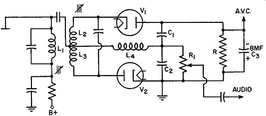
Fig. 9.24. Practical form of the ratio detector.
The practical form of the radio detector is shown in Fig. 9.24. It uses the phase-shifting properties of the discriminator of Fig. 9.13. R and C3 take the place of Eb, and the voltage developed across R will be dependent upon the strength of the incoming carrier. Note that V1 and V 2 form a series circuit with R ( and C3) and any current flowing through these tubes must flow through R. However, by shunting the 8-mf electrolytic capacitor across R we maintain a fairly constant voltage. Thus, momentary changes in carrier amplitude are merely absorbed by the capacitor. It is only when the average value of the carrier is altered that the voltage across R is changed. The output audio frequency voltage is still taken from across C2 by means of the volume control.
Since the voltage across R is directly dependent upon the carrier strength, it may also be used for A.V.C. voltage. The polarity of the voltage is indicated in Fig. 9.26. With this detector, it becomes possible to design an FM receiver containing only two I.F. stages. The reduction in costs is consider able and permits marketing FM sets in a range comparable to the present AM receivers. The detector possesses the disadvantage of being more difficult to align, and greater care must be taken to obtain a linear characteristic. Distortion tends to become more noticeable at high input voltages, although this can be minimized by special compensations of the circuit.
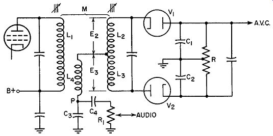
Fig. 9.25. A symmetrical ratio detector.
Ratio Detector Modifications. The ratio discriminator shown in Fig. 9.24 represents but one form of this circuit. In Fig. 9.25 there is a modification which possesses greater symmetry. Furthermore, it has the advantage of making available a voltage which can be used, in conjunction with a tuning eye, to indicate when the station is properly tuned in. L1, L2, and L3 are inductively coupled, which is similar to the previous discriminators.
However, in place of the former, direct capacitative connection between L1 and the secondary coil center-tap, we now have L4. It will be remembered that it is due to the presence of E1 in the secondary as a reference voltage that this circuit is able to function. In Fig. 9.25, we have, by using L4, substituted it for the previous method of obtaining this reference potential. L4 consists of several turns of wire which are closely coupled to L1. Hence, the voltage induced in L4 will remain constant so long as the primary voltage is constant. Since ET,4 depends upon E1 and not upon the secondary circuit, it can be used as the reference voltage in place of the previous arrangement.
If E L4 is varied, it would not affect the relative amplitudes or phases of any of the secondary voltages.
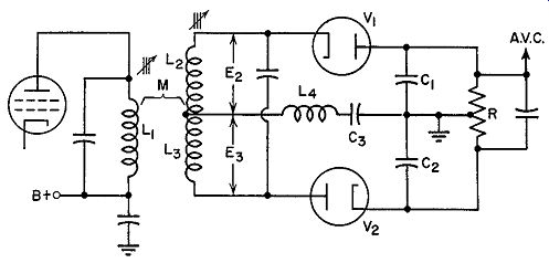
Fig. 9.26. The circuit of Fig. 9.25 rearranged to better indicate its
mode of operation.
To understand better the other modifications, the circuit of Fig. 9.25 has been rearranged (see Fig. 9.26). The path from the center tap on the secondary coil to the connection between 0 1 and 0 2 contains L4 and Ga. Disregard 0 4 and R1 for the moment, as they are merely placed across 0 3 to feed the audio output to the following amplifiers. The voltage which is applied to V1 consists of EL4 and E2. Across V2 we have EL4 and Ea. At the center I.F. value, both tubes receive the same voltage, with C1 and C2 charging to the same potential. But what of the potential across Ca?
At this moment it is zero. The reason can be found if we trace the current paths for each tube. The current in V2 flows up through L3, through L4 to C3 and C2. Current will flow in this path until the voltage across Ca and C2 equal the voltage across the tube. Then the flow ceases. The current from V1 will flow from its plate to C1 and Ca, then L4 and finally up through L2 to V1 again. As before, there will be a movement of electrons around this path until C1 and C3 charge to the potential at the tube. Note, however, that the current from V2 flows through L4 and C3 in a direction opposite to the current produced by V1 . Hence, what actually happens is that these two currents in the middle branch buck each other. At mid-frequency the result ant is zero. The voltage across C3 , then, is also zero. Hence, the current in the circuit flows from V2 , through L3 and L2 to V1 and through C1 and C2 back to V2. At mid-frequency, point P, Fig. 9.25, is zero with respect to ground.
At other frequencies, the voltage applied to each tube will differ with the result that a net current flows through C3 and L4. Which way the current flows will depend upon which tube receives the greater voltage. It is thus evident that the potential variations across C3 will vary directly with frequency and consequently represent the audio or demodulated voltage. By means of a coupling capacitor and a volume control, we can feed these audio variations to the succeeding amplifiers.
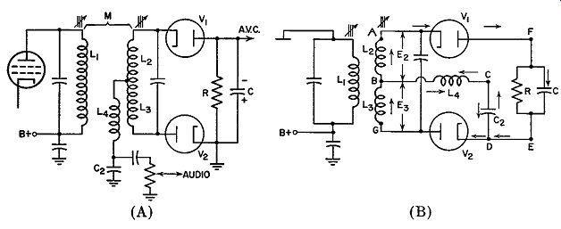
Fig. 9.27 (A). Another form that the ratio detector can assume.
(B) A rearrangement of Fig. (A).
Another arrangement of the ratio detector is shown in Fig. 9.27 A. This is similar to the circuit of Fig. 9.24 except that capacitor C2 has been retained and C1 has been eliminated. The audio voltage is obtained from C2, the same as in Fig. 9.24. L4 is coupled to L1 and furnishes the reference voltage which causes the potentials applied to V 1 and V2 to change with frequency.
In order to understand the operation of the circuit without C1, it must be kept in mind that the voltage across C2 is determine by:
1. The potential of R and C. This, in turn, is fixed by the average amplitude of the incoming FM signal.
2. The frequency of the incoming signal.
3. The relative currents flowing through V1 and V 2. This, of course, depends upon No. 2.
To demonstrate better the various current paths in the secondary net work, the rearranged diagram of Fig. 9.27B will be used. Note that no connections have been altered, merely the relative placement of several components.
The voltage applied to V2 is the vector sum of EL4 and Es (see Figs. 9.18 and 9.20). Similarly, the voltage active across V 1 is composed of EL4 and E2. As the frequency shifts in response to modulation, the total voltages at V1 and V 2 will follow suit. This has already been noted in previous paragraphs.
Consider, now, the current paths for each of the tubes. V1 is part of the complete path AFEDCBA. Its current can also flow through path AFEDGBA. For V2 , the two paths are: GBAFEDG and GBCDG. In other words, currents from each tube can flow around the outer path (GBAF-EDG) or part of each can be diverted through L4 and C2 of the center path.
When the total voltages applied to each tube are equal (at mid-frequency), no current flows through L4 and C2. This is true in all ratio detectors. At points other than mid-frequency, however, the current of one tube is greater and a portion of it does pass through L4 and C2. Hence, the voltage across C 2 will be a function of frequency. Due to the fact that each tube is connected into the circuit in an opposite manner, their currents (from V1 and V2) flowing through L4 and C 2 will likewise be opposite. Consequently, Ec2 will possess one polarity for frequencies above resonance and the opposite polarity for frequencies below resonance. By attaching a potentiometer across C2 , we can obtain an audio voltage for the audio amplifiers.
It may not be amiss at this point to note again the difference between the ratio detector and its predecessor in Fig. 9.5. The latter unit operates on the difference of the output voltages of two diode detectors. The diode load resistors are connected with their voltages opposing each other. The resultant of these two then becomes the output audio voltage. The response of this discriminator to amplitude modulation requires that a limiter (at least one) always precede it. Consequently, a comparatively large amount of amplification must be available so that the signal can be in a position to drive the limiter to saturation. Economically, this requirement raises the price of the receiver.
In the ratio detector, the two diodes are connected in series, and a controlling voltage is established in the circuit which is dependent upon the average value of the incoming carrier. Because of the long time-constant of the R-C filter in the network, instantaneous changes in signal amplitude are prevented from affecting the audio output voltage. Furthermore, this control voltage sets the limit to the maximum audio voltage than can be obtained. The ratio detector is more immune to amplitude modulation than the Foster-Seeley discriminator if the latter is considered by itself, without any limiter. However, when a limiter is added, the Foster-Seeley circuit possesses a slight edge in performance. The ratio detector, however, is more desirable economically since the amplification required ahead of this stage is less and advantage can be taken of this fact to reduce the number of stages in the I.F. system. Many manufacturers attempt a compromise by having the I.F. amplifier preceding the ratio detector operate as a partial limiter. While this reduces the gain of the I.F. system, it does improve the performance of the detector for FM signals possessing large amounts of amplitude modulation.
+++++++++++