AMAZON multi-meters discounts AMAZON oscilloscope discounts
The use of the electronic breadboard permits easy access to circuit components for measuring circuit parameters, such as voltage, current, and resistance. Also, the components can be easily replaced or rearranged until the optimum circuit performance has been obtained.
In the pages that follow, we will take a look at a number of breadboard techniques that are simple and inexpensive.
Breadboards for both vacuum-tube and transistor circuits are covered. Finally, two unique "integral-power supply" breadboards are described.
BREADBOARDS FOR VACUUM TUBE CIRCUITS
One of the simplest breadboard arrangements for vacuum-tube circuitry is shown in FIG. 1. A sheet of aluminum, the size of which depends on the number of components-tubes, capacitors, transformers, etc.-to be used, is selected. According to the design, the required number of tube socket holes, transformer mounting holes, and filter capacitor holes are cut or punched into the sheet.
Holes are drilled to accommodate insulated tip jacks which are placed around the components-a tip jack for each terminal of each component. For example, an 8-contact octal tube base will have eight tip jacks placed around it as shown.
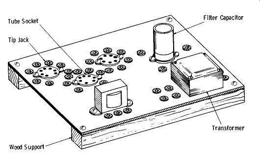
FIG. 1. Simple breadboard chassis.
The components are then mounted on the plate, and leads are run from the component terminals, transformers, etc. to their respective tip jacks.
Finally, the ends of the chassis plate are supported on small wood blocks so that the component terminal on the bottom of the chassis will not rest on the work surface.
We now have a unit with which we can, by using the tip jacks, connect in any desired arrangement, the components mounted on the chassis breadboard. The required smaller components, such as carbon resistors and tubular capacitors, are supplied with pin plugs for insertion into the tip jacks, as shown in FIG. 2. Various length leads for connections between tip jacks are made as shown in FIG. 2B.
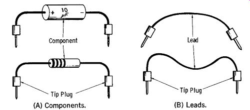
FIG. 2. Tip plugs on component leads. (A) Components. (B) Leads.
A Wooden Breadboard
FIG. 3 shows a simple electronic breadboard. This type of breadboard is used to quickly assemble an experimental circuit without the necessity of punching and drilling holes in a metal chassis.
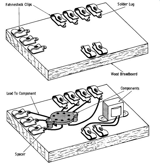
FIG. 3. Wooden breadboards.
Fahnestock clips, rather than pin jacks, are used to make connections to the various component tie points. These clips are simply screwed to the board with small round-head wood screws. A solder lug is placed under the head of each screw to provide the electrical connection to the Fahnestock clip.
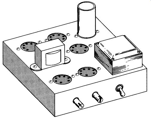
FIG. 4. Permanent breadboards.
The tube sockets and all other components that have either leads or terminals coming from their undersides are mounted to the board with metal spacers.
Still another approach to the electronic breadboard is shown in FIG. 4. Several tube sockets, as well as any trans-formers, chokes, filter capacitors, etc., which are anticipated in any circuit project are mounted on the chassis. The result is a chassis with a sufficient number of components to assemble any present or anticipated project.
This type of breadboard permits the use of short, direct connections between components-a necessity when working with high-frequency or high-gain audio circuits.
FIG. 5 is an example of component wiring, showing the underneath side of the chassis in FIG. 4.
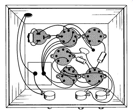
FIG. 5. Example of component wiring.
An Integral-Power Supply Breadboard for Vacuum-Tube Projects
Here is a rather novel type of electronic breadboard which contains an integral regulated power supply to furnish all necessary operating voltages, heater, plate, and bias for experimental vacuum-tube circuits.
FIG. 6 shows the physical arrangement of the regulated power supply breadboard. A standard 13" X 17" X 3" aluminum metal chassis is used as the basic breadboard. A portion of the chassis is cut out as shown, leaving an opening on which an aluminum plate may be installed. This removable plate serves as the breadboard on which the developmental circuit is assembled. The completed bread board plate may be removed from the basic foundation chassis and a new plate substituted.
The regulated power supply is capable of supplying 6.3 volts at 2 amperes, 300 volts at 50 mA, regulated and vari able, and 400 volts at 200 mA. The two high-voltage de outputs cannot be drawn simultaneously.
FIG. 7 is the schematic diagram of the regulated power supply. The supply consists of three basic sections-a power transformer and filter, voltage regulator, and bias supply.
The operation of the supply is as follows: When 120 volts is applied to the primary of T1, a high voltage is developed across the secondary winding which is applied to the full-wave rectifier V1. There is also a 6.3-volt winding which is applied to the 6.3-volt output terminals of the supply, and a 5-volt winding which supplies heater power for the full-wave rectifier.
The rectified output from V1 is applied to the choke input filter made up of L1 and C1. (A choke-input filter was chosen to enhance the regulation of the +400-volt output.) The output from the filter is applied to both the 400-volt output terminal and to the plate of the series regulator tube, V2. The cathode of V2 is connected to the +Regulated output terminal.
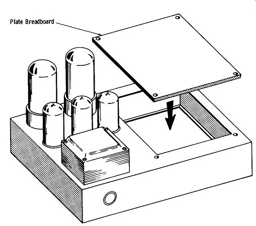
FIG. 6. Integral power-supply breadboard.
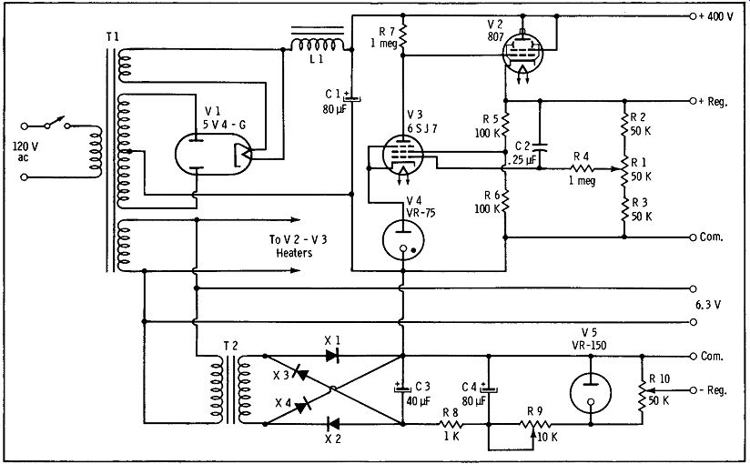
FIG. 7. A voltage divider, consisting of R1, R2, and R3, is placed from
the cathode of V2 to ground (common). The voltage-control potentiometer,
R1, selects a portion of the voltage developed across the voltage divider
and applies it to the control grid of the error amplifier, V3.
The cathode of V3 is held at a constant voltage by the gaseous voltage regulator, V 4.

------ Table 1 . Parts List for FIG. 7
Item No. Description
C1 80 µF, 450 volt electrolytic capacitor
C2 .25 µF, 600 volt paper capacitor
C3 40 µF, 150 volt electrolytic capacitor
C4 80 µF, 150 volt electrolytic capacitor
RESISTORS
R1 50K, 1 watt carbon potentiometer (linear taper)
R2 50K, 1 watt carbon fixed resistor
R3 50K, 1 watt carbon fixed resistor
R4 1 meg, 1 watt carbon fixed resistor
R5 100K, 1 watt carbon fixed resistor
R6 100K, 1 watt carbon fixed resistor
R7 1 meg, 1 watt carbon fixed resistor
R8 1K, 5 watt wirewound resistor
R9 10K, 5 watt potentiometer
R10 50K, 5 watt potentiometer
TUBES
V1 5V4G tube
V2 807 tube
V3 6SJ7tube
V4 VR-75 tube
V5 VR-150 tube
TRANSFORMERS
T1 Power transformer (Stancor PC-8412, or equiv.)
T2 Low-voltage transformer (Stancor P-6134, or equiv.)
CHOKE
L1--Filter choke (Stancor C-1001, or equiv.)
DIODES
X1, X2, X3, X4--1N1222 silicon diode (or 1N4004)
--------
The amplified error signal is applied to the control grid of the series tube, V2, where it controls the amount of current applied to the load.
In operation, if an increase in load current occurs, the voltage developed across the voltage divider, R1-R2-R3, will drop. Likewise, the voltage at the slider of the voltage-control potentiometer, R2, will drop, lowering the positive voltage applied to the control grid of the error amplifier, V3.
Since the cathode of V3 is held at a constant voltage by the voltage reference tube, V 4, the control grid of V3 becomes less positive with respect to its cathode. This will decrease the V3 plate current, resulting in a smaller voltage drop across plate load resistor R7. This decreased voltage drop across R7 will cause the plate of V3 to become more positive.
Since the plate of V3 is directly connected to the control grid of V2, this control grid will become more positive with respect to its cathode, and V2 will allow more voltage to be developed across the load. Should the load voltage rise, the reverse of the foregoing action will occur.
BREADBOARDS FOR SEMICONDUCTOR CIRCUITS
The techniques involved in semiconductor breadboarding are necessarily different than those for vacuum tubes. The smaller physical size of semiconductors and their related components allows different breadboarding techniques.
Typical Semiconductor Breadboards FIG. 8 shows a representative type of breadboard de signed for use with semiconductor devices.
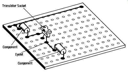
FIG. 8. Perforated-board breadboard.
The breadboard is usually made of perforated phenolic.
Electrical and mechanical tie-points are formed with brass eyelets. Component leads are inserted through these eyelets and soldered in place. For minimum wear on transistor leads, transistor sockets may be used, with the socket terminals brought out to eyelets for making connections to the other circuit components.
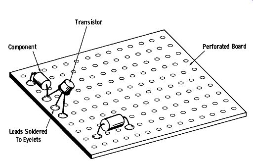
FIG. 9. Variation of FIG. 8.
FIG. 9, a variation of FIG. 8, shows the semiconductors soldered directly to the eyelet tie-points.
Commercially Available Breadboards
Several manufacturers market electronic breadboards at reasonable costs. FIG. 10 shows one example.
In addition to the complete breadboard kits, there are individual components designed especially for breadboarding setups. FIG. 11 shows a few of these.
An Integral Power Supply Breadboard For Semiconductors
This integral breadboard is similar to the vacuum-tube integral power supply breadboard described earlier. however, this breadboard is designed especially for semiconductor circuit development.
As shown in FIG. 12, the integral power supply bread board consists of a variable low-voltage de power supply mounted at one end of an aluminum chassis. A portion of the chassis opposite the supply is cut out so that a piece of perforated board may be mounted.
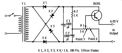
FIG. 13 is the schematic diagram of the regulated power supply. Let's
briefly examine its operation.
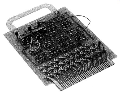
FIG. 10. Commercial breadboard.
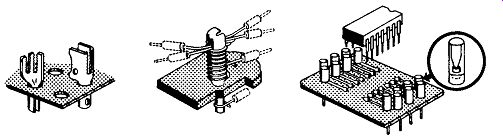
Fig. 11 Commercial breadboard components.
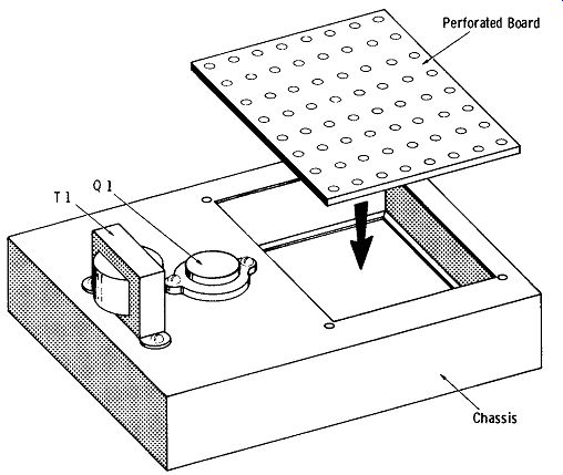
FIG. 12. Integral power-supply breadboard.
FIG. 13. Low-voltage power supply.
When 120 volts are applied to the primary of the power/ isolation transformer T1, 25 volts are developed across the secondary and applied to the full-wave bridge rectifier, consisting of X1, X2, X3, and X4. The pulsating direct-current output from the rectifier is filtered by C1.
The negative voltage output from the rectifier is applied to the collector of transistor Q1. The collector of Q1 is connected to the negative output terminal of the supply.
The negative output from the rectifier is also applied to the voltage divider, R1 and R2. A second filter capacitor (C2) is connected at the junction of R1 and R2 which further enhances the filtering. The slider of the voltage-control-potentiometer, R1, is connected to the base of Q1.
As the slider of R1 is varied, the voltage applied to the base of Q1 is also varied from 0 volts to approximately 23 volts.
In operation, when the slider of R1 is set at point X, the base of Q1 receives no current and Q1 is cut off. Since there is no current through Q1, there will be no voltage at the supply output terminals.
As the slider of R2 is moved toward point Y the base bias applied to Q1 will increase from 0 mA, and Q1 will become forward-biased. As a result, there will be collector current through Q1, and a voltage will be developed across the output terminals of the supply. The amount of base bias for Q1 and hence the supply's output is thus determined by the setting of R1.
The supply will furnish an output voltage ranging from 0 to 20 volts, at 200 mA, and somewhat higher at loads below 50 mA.
Also see: Basics of Electricity and Electronics with Projects
AMAZON multi-meters discounts AMAZON oscilloscope discounts