ADVANCED AMPLIFIER DESIGNS
In normal amplifier systems, based on a straightforward application of negative feedback, the effective circuit can be considered as comprising four parts:
• the output power stages, which will normally be simple or compound emitter followers, using power MOSFETs or bipolar transistors, using one of the forms shown in Figs 17(a)-(f):
• the voltage amplifying circuitry;
• the power supply system; and
• the protection circuitry needed to prevent damage to the output devices or the LS load.
The choice made in respect of any one of these will influence the requirements for the others.
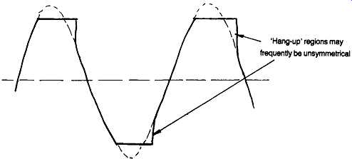
FIG. 16 Effect of 'hang-up' following clipping. Hang-up* regions may frequently
be unsymmetrical
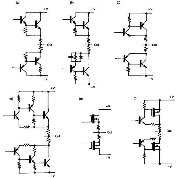
FIG. 17 Output transistor circuits.
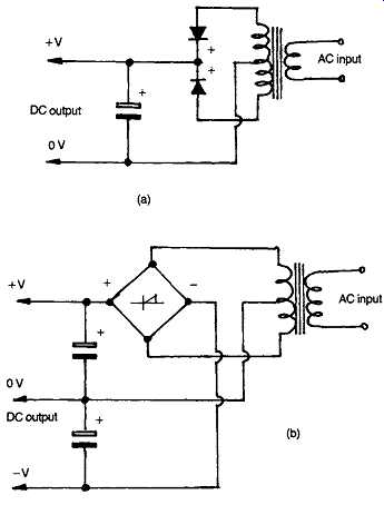
FIG. 18 Simple DC power supplies.
Power supply systems
It has, for example, been common practice in the past to use a simple mains transformer, rectifier and reservoir capacitor combination of the kind shown in Figs 18(a) and (b), to provide the DC supply to the amplifier. This has an output voltage which will decrease under increasing load, and it’s necessary to know the characteristics of this supply in order to be able to specify the no-load output voltage which will be necessary so that the output voltage on maximum load will still be adequate to provide the rated output power.
Again, it’s probable that the power supply for any medium to high power amplifier will provide more than enough current to burn out an expensive LS system in the event of an output transistor failure in the power amplifier, so some output fuse will be required. Unfortunately, most fuse holders tend to have a variable contact resistance, which introduces an unwelcome uncertainty into the critical LS output circuit.
The presence of the mains frequency-related AC ripple on the supply lines from such a simple power supply circuit, which will become worse as the output power to the load is increased, means that the voltage amplification circuitry must be chosen to have an adequate rejection of the supply line ripple.
Also, due to the relatively high circuit impedance, signal components present on the supply lines will worsen the distortion characteristics of the circuit if they break through into the signal path, since in a Class B or AB system these components will be highly distorted.
Such signal intrusion can also cause unwanted inter-channel breakthrough, and encourage the use of entirely separate power supply systems.
Such simple power supplies may carry hidden cost penalties, too, since the working voltage rating of the power transistors must be adequate to withstand the no-load supply potential, and this may demand the use of more expensive, high-voltage transistors having relatively less good current gain or high frequency characteristics.
Stabilized power supplies
If, on the other hand, an electronically stabilized power supply is used, the output voltage can be controlled so that it’s the same at full output power as under quiescent current conditions, and largely independent of mains voltage. Moreover, the supply can have a 're-entrant' overload characteristic, so that, under either supply line or LS output short-circuit conditions, supply voltage can collapse to a safely low level, and a monitor circuit can switch off the supplies to the amplifier if an abnormal DC potential, indicating output transistor failure, is detected at the LS terminals. Such protection should, of course, be fail-safe.
Other advantages which accrue from the use of stabilized power supplies for audio amplifiers are the low inherent power supply line 'hum' level, making the need for a high degree of supply line ripple rejection a less important characteristic in the design of the small signal stages, and the very good channel-to-channel isolation, because of the low inherent output impedance of such systems.
The principal sonic advantages which this characteristic brings are a more 'solid' bass response, and a more clearly defined stereo image, because the supply line source impedance can be very low, typically of the order of 0.1 ohms. In a conventional rectifier/capacitor type of power supply, a reservoir capacitor of 80000 µF would be required to achieve this value at 20 Hz. The inherent inductance of an electrolytic capacitor of this size would give it a relatively high impedance at higher frequencies, whereas the output impedance of the stabilized supply would be substantially constant.
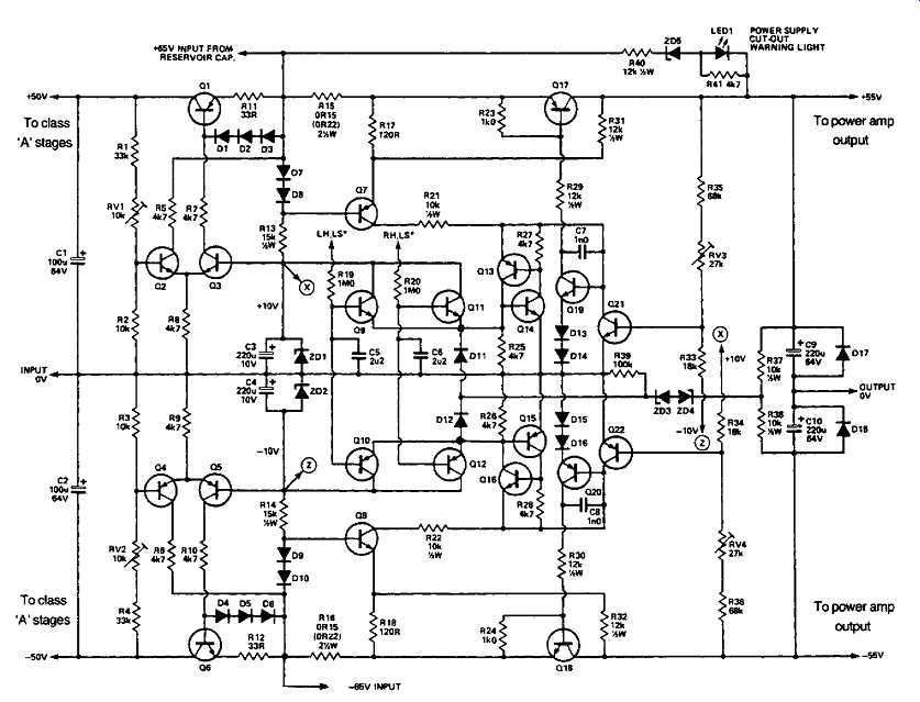
FIG. 19 Twin dual-output stabilized power supply, with re-entrant overload
protection and LS offset shut-down, by Linsley Hood.
The design of stabilized power supplies is beyond the scope of this SECTION, but a typical unit, giving separate outputs for the power output and preceding voltage amplifier stages of a power amplifier, and offering both re-entrant and LS voltage offset protection, is shown in FIG. 19.
LS protection circuitry
This function is most commonly filled by the use of a relay, whose contacts in the output line from the amplifier to the LS unit are normally open, and only closed by the associated relay operating circuitry if all the appropriate conditions, including LS terminal DC offset and output load impedance, are within satisfactory limits.
Such circuitry is effective, but the relay contacts must have adequate contact area, and the relay must either be hermetically sealed or the contacts must be plated with gold or equivalent noble metal to preserve a low value of contact resistance in the presence of atmospheric contamination.
Output stage emitter follower configurations
Various circuit forms have been adopted for this purpose, of which the more useful -ones are shown in FIG. 17. The actual form is known to have a bearing on the perceived sound quality of the design, and this was investigated by Otala and Lammasneimi (Wireless World, December 1980), who found that, with bipolar transistors, the symmetrical compound emitter follower circuit of FIG. 17(c) was significantly better than the complementary Darlington configuration of FIG. 17(a), in terms of the amplifier's ability to reject distortion components originating in load non linearities from, or electromagnetic signal voltages originating in, the LS unit.
The actual desirable criterion in this case is the lowness of the output impedance of the output emitter follower configuration before overall negative feedback is applied to the amplifier, the point being that the feedback path within the amplifier is also a path whereby signals originating outside the amplifier can intrude within the signal path.
The major advantages offered by the use of power MOSFETs, typically in one or other of the configurations shown in Figs 17(e) or (f), are their greater intrinsic linearity in comparison with bipolar junction transistors, and their much higher transition frequency, which simplifies the design of a stable feedback amplifier having a low harmonic distortion.
On the other hand, the output impedance of the simple source follower is rather high, and this demands a higher gain from the preceding voltage amplifier stage if an equivalent overall performance is to be obtained.
The inclusion of a low value resistor in the output circuit of the amplifier, between the emitter follower output and the LS load, as shown in the (1972) 75 W amplifier of FIG. 7, greatly reduces this type of load induced distortion and is particularly worth while in the case of the circuit layouts shown in Figs 17(a) and (e).
Power amplifier voltage gain stages
The general design systems employed in transistor gain stages have been examined in SECTION 4. However , for high quality audio power amplifiers higher open-loop stage gains, and lower inherent phase shift characteristics, will be required -- to facilitate the use of large amounts of overall NFB to linearize output stage irregularities -- than is necessary for the preceding small signal gain stages.
Indeed, with very many modern audio amplifier designs, the whole of the small signal pre-amplifier circuitry relies on the use of good quality integrated circuit operational amplifiers, of which there are a growing number which are pin compatible with the popular TL071 and TL072 single and dual FET-input op. amps. For power amplifier voltage stages, neither the output voltage nor the phase shift and large signal transient characteristics of such op-amps are adequate, so there has been much development of linear voltage gain circuitry , for the 'Class A' stages of power amplifiers, in which the principal design requirements have been good symmetry, a high gain/bandwidth product, a good transient response, and low-phase shift values within the audio range.
A wide range of circuit devices, such as constant current sources, current mirrors, active loads and 'long-tailed pairs' have been employed for this purpose, in many ingenious layouts. As a typical example, the circuit layout shown in FIG. 20, originally employed by National Semiconductors Inc. in its LH0001 operational amplifier, and adopted by Hitachi in a circuit recommended for use with its power MOSFETs, offers a high degree of symmetry, since O3/Q4, acting as a current mirror, provide an active load equivalent to a symmetrically operating transistor amplifier, for the final amplifier transistor, Q6.
This circuit offers a voltage gain of about 200000 at low frequencies, with a stable phase characteristic and a high degree of symmetry. The derivation and development of this circuit was analyzed by the author in Wireless World (July 1982). An alternative circuit layout, of the type developed by Hafler, has been described by E. Borbely (Wireless World, March 1983), and is shown in FIG. 21. This is deliberately chosen to be fully symmetrical, so far as the transistor characteristics will allow, to minimize any tendency to slew rate limiting of the kind arising from stray capacitances charging or discharging through constant current sources. The open/loop gain is, however, rather lower than of the NS/Hitachi layout of FIG. 20. Both unbypassed emitter resistors and base circuit impedance swamping resistors have been freely used in the Borbely design to linearize the transfer and improve the phase characteristics of the bipolar transistors used in this design, and a further improvement in the linearity of the output push-pull Darlington pairs (Qs/CVCVQ«)) is obtained by the use of the 'cascode' connected buffer transistors Q7 and Q10.
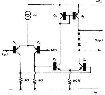
FIG. 20 Symmetrical high gain stage.
The particular merit of the cascode layout in audio circuitry is that the current flow through the cascode transistor is almost entirely controlled by the driver transistor in series with its emitter. In contrast, the collector potential of the driver transistor remains virtually constant, thus removing the deleterious effect of non-linear internal voltage dependent leakage resistances or collector-base capacitances from the driver device.
The very high degree of elaboration employed in recent high-quality Japanese amplifiers in the pursuit of improvements in amplifier performance, is shown in the circuit of the Technics SE-A100 voltage gain stage, illustrated in a somewhat simplified form in FIG. 22.
In this, an input long-tailed pair configuration, based on junction FETs (Q1, Q4 with CC1), to take advantage of the high linearity of these devices, is cascode isolated (by Q2, Q3) from a current mirror circuit, (CM!), which combines the output of the input devices in order to maximize the gain and symmetry of this stage, and drives a PNP Darlington pair amplifier stage (Q5, Q6). The output transistor, Q6, drives a current mirror (CM2) through a cascode isolating transistor (Q7) from Q6 collector, and a further cascode isolated amplifier stage (Q8, Q9) from its emitter , for which the current mirror CM2 serves as an active load. The amplified diode transistor, Q10, serves to generate a DC offset potential, stabilized by a thermistor, (???), to forward bias a succeeding push-pull pair of emitter followers.
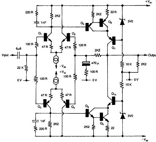
FIG. 21 Symmetrical push-pull stage by Borbely.
As a measure of the effectiveness of this circuit elaboration, the quoted harmonic distortion figures , for the whole amplifier, are typically of the order of 0.0002%.
ALTERNATIVE DESIGN APPROACHES
The fundamental problem in any 'Class B' or ' Class AB' transistor amplifier is that some non-linearity inevitably exists at the region where the current flow through one output transistor turns on and the other turns off.
This non-linearity can be minimized by the careful choice of output stage quiescent current, but the optimum performance of the amplifier depends on this current value being set correctly in the first place, and on its remaining constant at the set value throughout the working life of the amplifier.
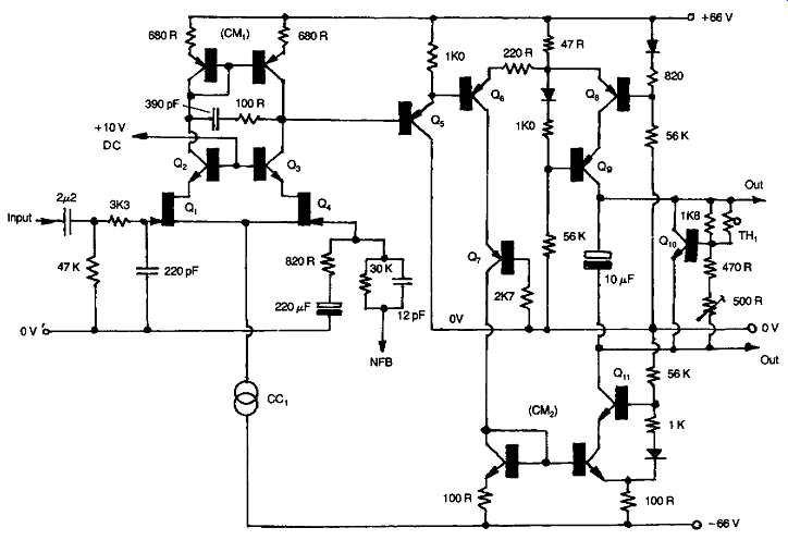
FIG. 22 Technics voltage gain stage.
One answer is, of course, to abandon ' Class AB' operation, and return to 'Class A', where both output transistors conduct during the whole AC output cycle, and where the only penalty for an inadvertent decrease in the operating current is a decrease in the maximum output power. The author's original four-transistor, 10 W 'Class A' design (Wireless World, April 1969) enjoys the distinction of being the simplest transistor operated power amplifier which is capable of matching the sound quality of contemporary valve designs. The problem, of course, is its limited power output.
The Blomley non-switching output circuit
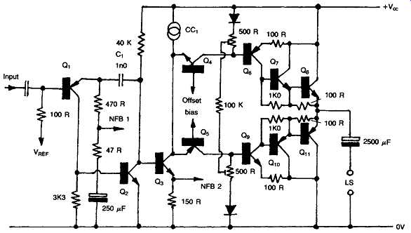
FIG. 23 The Blomley non-switching push-pull output stage.
The possibility of achieving a higher power 'Class AB' or even 'Class B' amplifier circuit, in which some circuit device is used to remove the fundamental non-linearity of the output transistor crossover region, in such circuits, is one which has tantalized amplifier designers for the past two decades, and various approaches have been explored. One of these which attracted a lot of interest at the time was that due to P. Blomley (Wireless World, February/March 1971), and which is shown, in simplified form, in FIG. 23.
In this, Q1, Q2, and Q3 form a simple three-stage voltage amplifier, stabilized at HF by the inclusion of capacitor C1 between Q2 collector and Ch emitter. The use of a constant current load (CQ) ensures good linearity from this stage. The crux of the design is the use of a pair of grounded base or cascode connected transistors, (Q4, Q5), whose bases are held, with a suitable DC offset between them, at some convenient mid-point DC level, which route the output current from the gain stage, Q3, to one or other of the push-pull output triples (Q6, Q7, Q8 and Q9, Q10, Q11) which are arranged to have a significant current gain and also to be forward-biased, and therefore conducting, during the whole of the output signal cycle.
Although acclaimed as a non-switching 'Class AB' output configuration, in reality, the switching of the output half cycles of a 'Class B' system still takes place, but through the small signal transistors Q4 and Q5 which, since they are freed from the vagaries of the output loudspeaker load, and the need to pass a substantial output current, may be assumed to do the switching more cleanly and rapidly. Nevertheless, the need to maintain an accurate DC offset between the bases of these switching transistors still remains, and errors in this will worsen residual crossover distortion defects.
The Quad current dumping amplifier design
This unique and innovative circuit, subsequently employed commercially in the Quad 405 power amplifier, was first disclosed by P. J. Walker and M. P. Albinson at the fiftieth convention of the Audio Engineering Society, in the summer of 1975, and a technical description was given by Walker later in the year (Wireless World, December 1975). This design claims to eliminate distortion due to the discontinuous switching characteristics of the unbiased, 'Class B', push-pull output transistor pair, by the use of a novel dual path feedback system, and thereby eliminate the need for precise setting-up of the amplifier circuit. It has been the subject of a very considerable subsequent analysis and debate, mainly hinging upon the actual method by which it works, and the question as to whether it does, or even whether it can, offer superior results to the same components used in a more conventional design.
What is not in doubt is that the circuit does indeed work, and that the requirement for correct adjustment of the output transistor quiescent current is indeed eliminated.
Of the subsequent discussion, (P. J. Baxandall, Wireless World, July 1976; Divan and Ghate, Wireless World, April 1977; Vanderkooy and Lipshitz, Wireless World, June 1978; M. McLoughlin, Wireless World, September/October 1983), the explanation offered by Baxandall is the most intellectually appealing, and is summarized below.
Consider a simple amplifier arrangement of the kind shown in FIG. 24(a), comprising a high-gain linear amplifier (??) driving an unbiased ('Class B') pair of power transistors (Q1 Q2), and feeding a load, ZL. Without any overall feedback the input/output transfer curve of this circuit would have the shape shown in the curve 'x' of FIG. 25, in which the characteristic would be steep from M' to N' while Q2 was conducting, much flatter between N' and N while only the amplifier ?? was contributing to the output current through the load, by way of the series resistance R3, and then steeper again from N to M, while Q1 was conducting.
If overall negative feedback is applied to the system via Ru the extent of the discontinuity in the transfer curve can be made less, especially if the closed loop gain of A! is sufficiently high, leading to a more linear characteristic of the type shown. However, it would still be unsatisfactory.
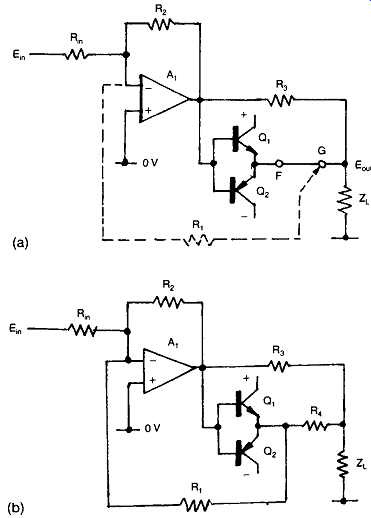
FIG. 24 The basic current dumping system.
What is needed is some way of increasing the negative feedback applied to the system during the period in which Ch and Q2 are conducting, to reduce the overall gain of the system so that the slope of the transfer characteristic of FIG. 25 is identical in the regions M' to N' and N to M to that between N' and N. This can be done by inserting a small resistor, (R4), between points F and G, in the output circuit of the push-pull emitter followers Ch and Q2, so that there will be a voltage drop across this resistor, when Q1 and Q2 are feeding current into the load, and then deriving extra negative feedback from this point, (F), which will be related to the increased current flow into the load.
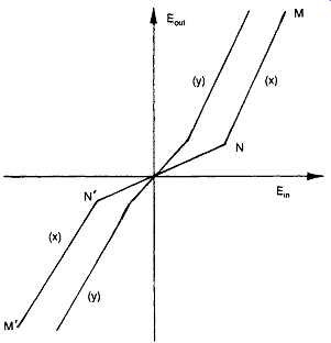
FIG. 25 Current dumping amplifier transfer characteristics.
If the values of R1, R2, R3 and R4 are correctly chosen, in relation to the open loop gain of ??, the distortion due to the unbiased output transistors will very nearly vanish, any residual errors being due solely to the imperfect switching characteristics of Q1 and Q2 and the phase errors at higher frequencies of the amplifier A^ Unfortunately, the output resistor, R4, in the LS circuit would be wasteful of power, so Walker and Albinson substitute a small inductor for this component in the actual 404 circuit, and compensate for the frequency dependent impedance characteristics of this by replacing R2 with a small capacitor.
While the amplifier circuit still works within the performance limits imposed by inevitable tolerance errors in the values of the components, this L and C substitution serves to complicate the theoretical analysis very considerably, and has led to a lot of the subsequent debate and controversy.
Feed-forward systems
The correction of amplifier distortion by the use of a comparator circuit, which would disclose the error existing between the input and output signals, so that the error could be separately amplified and added to or subtracted from the voltage developed across the load, was envisaged by H. S. Black, the inventor of negative feedback, in the earlier of his two US Patents (1686792/1928). Unfortunately, the idea was impracticable at that time because sufficiently stable voltage amplifiers were not obtainable.
However, if such a system could be made to work, it would allow more complete removal of residual errors and distortions than any more conventional negative feedback system, since with NFB there must always be some residual distortion at the output which can be detected by the input comparator and amplified to reduce the defect. In principle, the 'feed forward' addition of a precisely measured error signal could be made to completely cancel the error, provided that the addition was made at some point, such as the remote end of the load, where it would not be sensed by the error detection system.
Two practical embodiments of this type of system by A. M. Sandman (Wireless World, October 1974), are shown in Figs 26(a) and (b). In the second, the iterative addition of the residual distortion components would allow the distortion in the output to be reduced to any level desired, while still allowing the use of a load circuit in which one end was connected to the common earth return line.
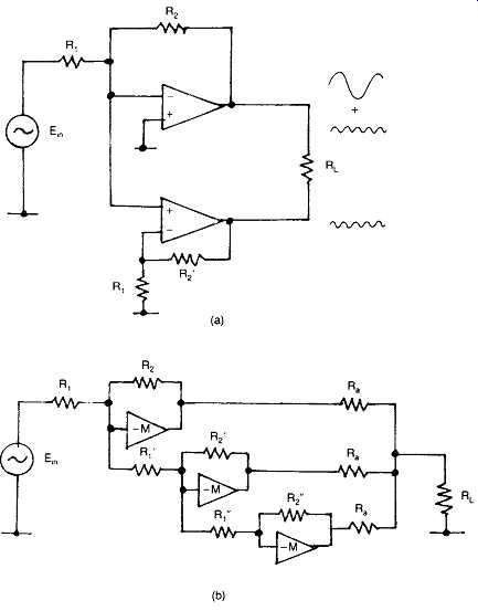
FIG. 26 Feed-forward systems for reducing distortion.
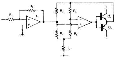
FIG. 27 Sandman's 'Class S' system.
'Class S' amplifier systems
This ingenious approach, again due to A. M. Sandman (Wireless World, September 1982), has elements in common with the current dumping system, though its philosophy and implementation are quite different. The method employed is shown schematically in FIG. 27. In this a low power, linear, 'Class A' amplifier, (A1) is used to drive the load (Zl) via the series resistor, R4. The second linear amplifier, driving the 'Class B' push-pull output transistor pair, Qi/Q2, monitors the voltage developed across R4, by way of the resistive attenuator, R5/R6, and adjusts the current fed into the load from Q1 or Q2 to ensure that the load current demand imposed on A1 remains at a low level.
During the period in which neither Q1 nor Q2 is conducting, which will only be at regions close to the zero output level, the amplifier A, will supply the load directly through R4. Ideally, the feedback resistor, R2, should be taken to the top end of Zl9 rather than to the output of A^ as shown by Sandman.
A modified version of this circuit, shown in FIG. 28, is used by Technics in all its current range of power amplifiers, including the one for which the gain stage was shown in FIG. 22. In this circuit, a high-gain differential amplifier, (A2), driving the current amplifier output transistors…
(Qi> Ch)* is fed from the difference voltage existing between the outputs of A1 and A2, and the bridge balance control, Ry, is adjusted to make this value as close to zero as practicable.
Under this condition, the amplifier A1 operates into a nearly infinite load impedance, as specified by Sandman, a condition in which its performance will be very good. However, because all the circuit resistances associated with R3, R4 and Rx are very low, if the current drive transistors are unable to accurately follow the input waveform, the amplifier A1 will supply the small residual error current. This possible error in the operation of Q1 and Q2 is lessened, in the Technics circuit, by the use of a small amount of forward bias (and quiescent current) in transistors Q1 and Q2.
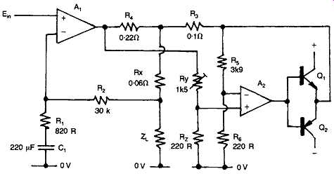
FIG. 28 Technics power amplifier circuit (SE-A100).
CONTEMPORARY AMPLIFIER DESIGN PRACTICE
This will vary according to the end use envisaged for the design. In the case of low cost 'music center types of system, the main emphasis will be upon reducing the system cost and overall component count. In such equipment, the bulk of the circuit functions, including the power output stages, will be handled by purpose built integrated circuits.
From the point of view of the manufacturers, these ICs and other specialized component groupings will be in-house items, only available from the manufacturer, and a more substantial profit margin on the sale of these to accredited repair agents will assist in augmenting the meager profit levels imposed by competitive pressures on the original sale of the equipment.
In more prestigious equipment, intended to be assessed against similar units in the hi-fi market, the choice of circuit will lie between designs which are basically of the form shown in FIG. 14, but using more elaborate first stage amplifier circuitry, and with either bipolar or power MOSFET transistor output devices, or more elaborate systems derived from the Blomley, Sandman, or Current Dumping designs, or on systems in which the amplifier quiescent current is automatically adjusted during the output cycle with the aim of keeping the output stages operating, effectively, in 'Class A', but without the thermal dissipation penalty normally incurred by this.
Many, but not all, of the better quality units will employ stabilized DC power supplies, and virtually all of the high quality designs will be of the so-called direct-coupled form, in which the LS output is taken directly from the mid-point of the output emitter followers, without the interposition of a DC blocking output capacitor. (The use of true DC coupling from input to LS output is seldom found because of the problems of avoiding DC offset drift.) Such direct-coupled amplifiers will, inevitably, employ symmetrical positive and negative supply lines, and in more up-market systems, the power supplies to the output stages will be separated from those for the preceding low power driver stages, and from any power supply to the preceding pre-amp circuitry. This assists in keeping cross-channel breakthrough down to a low level, which is helpful in preserving the stability of the stereo image.
Great care will also be exercised in the best of contemporary designs in the choice of components, particularly capacitors, since the type of construction employed in these components can have a significant effect on sound quality. For similar reasons, circuitry may be chosen to minimize the need for capacitors, in any case.
Capacitors:
Although there is a great deal of unscientific and ill-founded folklore about the influence of a wide variety of circuit components, from connecting wire to the nature of the fastening screws, on the final sound quality of an audio amplifying system, in the case of capacitors there is some technical basis for believing that imperfections in the operational characteristics of these components may be important, especially if such capacitors are used as an integral part of a negative feedback comparator loop.
The associated characteristics which are of importance include the inherent inductance of wound foil components, whether electrolytic or non-polar types, the piezo-electric or other electromechanical effects in the dielectric layer, particularly in ceramic components, the stored charge effects in some polymeric materials, of the kind associated with 'electret' formation, (the electrostatic equivalent of a permanent magnet, in which the material retains a permanent electrostatic charge), and non-linearities in the leakage currents or the capacitance as a function of applied voltage.
Polypropylene film capacitors, which are particularly valued by the subjective sound fraternity, because of their very low dielectric loss characteristics, are particularly prone to electret formation, leading to an asymmetry of capacitance as a function of polarizing voltage. This effect is small, but significant in relation to the orders of harmonic distortion to which contemporary designs aspire.
Care in the decoupling of supply lines to the common earth return line is also of importance in the attainment of high performance, as is care in the siting and choice of earth line current paths. Such aspects of design care are not disclosed in the electronics circuit drawings.
SOUND QUALITY AND SPECIFICATIONS
Most of the performance specifications which relate to audio systems - such as the power output, (preferably measured as a continuous power into a specified resistive load), the frequency response, the input impedance and sensitivity, or the background noise level in comparison to some specified signal level - are reasonably intelligible to the non-technical user, and capable of verification on test.
However, the consideration which remains of major interest to the would-be user of this equipment is what it will sound like, and this is an area where it’s difficult to provide adequate information from test measurements.
For example, it has been confidently asserted by well-known engineers that all competently designed power amplifiers operated within their ratings will sound alike. This may be true in respect of units from the same design stable, where the same balance of compromises has been adopted by the designer, but it’s certainly untrue in respect of units having different design philosophies, and different origins.
As a particular case in point, until the mid-1970s a large majority of commercial designs employed a second-stage slew-rate limiting capacitor, in the mode discussed above, as a means of attaining stable operation without sacrifice of THD characteristics at the upper end of the audio band.
The type of sonic defect produced by slew-rate limiting is unattractive, and clearly audible by any skilled listener who has trained his ears to recognize the characteristic degradation of sound quality due to this.
Since the publicity given to transient intermodulation distortion by Otala, this type of stabilization is now seldom used in feedback amplifiers and other, technically more correct, methods are now more generally employed.
Since this type of shortcoming is now recognized, are we to accept that those of the preceding generation of designs which suffered from this defect (and which, in many cases, originated from the drawing boards of those same engineers who denied the existence of any differences) were, indeed, incompetently designed?
Design compromises:
Unfortunately, the list of desirable parameters relating to the sound quality of audio amplifiers is a long one, and some of the necessary specifications are imperfectly understood. What is beyond doubt is that most of the designers operating in this field are well aware of their inability to attain perfection in all respects simultaneously, so that they must seek a compromise which will necessarily involve the partial sacrifice of perfection in one respect in order to obtain some improvement in some other mutually incompatible region.
The compromises which result, and which have an influence on the amplifier sound, are based on the personal judgment or preferences of the designer, and will vary from one designer to another.
An example of this is the case of low harmonic distortion figures at higher audio frequencies, and good transient performance and freedom from load induced instability, in a feedback amplifier. These characteristics are partially incompatible. However, THD' figures are prominently quoted and form an important part of the sales promotion literature and the reviewers report. Considerable commercial pressure therefore exists to attain a high performance in this respect.
Transient characteristics and feedback loop stability margins are not quoted, but shortcomings in either of these can give an amplifier a 'hard' or 'edgy' sound quality and it’s not uncommon for poor amplifier transient performance to lead to a redistribution of energy in the time domain or the frequency spectrum which may amount to as much as a quarter of the total transient energy.
Bearing in mind the importance of good behavior in this respect, it’s to be regretted that if the transient performance of an amplifier is shown at all, it’s likely to be shown only as a response to symmetrical square waves, rather than to the more complex asymmetrical transients found in program material.
Measurement systems
A measurement system which attempts to provide a more readily quantized technique for assessing amplifier performance, in the hope of lessening the gap which exists between existing performance specifications -- which mainly relate to steady state (i.e., sinusoidal) test signals -- and the perceived differences in amplifier sound, has been devised by Y. Hirata (Wireless World, October 1981). This technique uses asymmetrical, pulse type, input signals which approach more closely in form to the kinds of transient pressure wave forms generated by , for example, a bursting balloon, a hand clap, or cracker. The changes in these test waveforms caused by a variety of amplifier faults is shown by Hirata, but the interpretation of the results is too complex for it to be likely to replace the ubiquitous, if misleading, harmonic distortion figure as a criterion of amplifier goodness.
A further type of measurement, being explored by the BBC, has been described by R. A. Belcher (Wireless World, May 1978) using pseudo random noise signals, derived by frequency shifting a 'comb filter' spectrum. This is claimed to give a good correlation with perceived sound quality, but is, again, too complex at the moment to offer an easily understood measurement by which a potential customer could assess the likely quality of an intended purchase.
Conclusions
The conclusion which can be drawn from this discussion is that harmonic distortion figures, on their own, offer little guidance about sound quality, except in a negative sense -- that poor THD figures, in the 'worse than 0.5%' category, are likely to lead to poor sound quality. Fortunately, the understanding by design engineers of the requirements for good sound quality is increasing with the passage of time, and the overall quality of sound produced, even by 'budget' systems, is similarly improving.
In particular, there is now a growing appreciation of the relationship between the phase/frequency characteristics of the amplifier and the sound-stage developed by a stereo system of which it’s a part.
There still seems to be a lot to be said for using the simplest and most direct approach, in engineering terms, which will achieve the desired end result -- in that components which are not included won’t fail, nor will they introduce any subtle degradation of the signal because of the presence of minor imperfections in their mode of operation. Also, simple systems are likely to have a less complex phase/frequency pattern than more highly elaborated circuitry.
For the non-technical user, the best guarantee of satisfaction is still a combination of trustworthy recommendation with personal experience, and the slow progress towards some simple and valid group of performance specifications, which would have a direct and unambiguous relationship to perceived sound quality, is not helped either by the advertisers frequent claims of perfection or the prejudices, sycophancy and favoritism of some reviewers.
On the credit side, the presence of such capricious critics, however unwelcome their views may be to those manufacturers not favored with their approval, does provide a continuing stimulus to further development, and a useful counter to the easy assumption that because some aspect of the specification is beyond reproach the overall sound quality will similarly be flawless.