THE IMPORTANCE OF THE POWER SUPPLY UNIT
In the early days of audio, when mains-powered amplifiers were based almost exclusively on the use of thermionic valves, very great attention was paid to the design of the power supply unit from which the amplifier was fed. This was mainly in order to reduce the extent of the 100 or 120 Hz mains 'hum' whose presence, to some degree, was an almost inevitable accompaniment to the audio output of the system.
In more recent times, when low-cost audio systems have been exclusively based on 'solid-state' devices (bipolar junction transistors or ICs) the relatively high degree of power supply line signal rejection -- referred to as PSRR (power supply rejection ratio) in the IC manufacturers' data sheets - normally found in solid-state circuitry has encouraged a much more off-hand approach to this aspect of system design. This is a mistake, in design terms, since the output signal, usually developed in respect of an 'earthy' 0-volt line, is applied to the load in series with the power supply unit. This is true, as shown in FIG. 1, whether the output is single-ended (as in FIG. 1(a)), or 'direct coupled, and balanced about the 0V rail (as shown in FIG. 1(b)). Failure to consider the way in which the output current flow path was completed led to a design oversight in a commercial 'pseudo-class A' amplifier which was analyzed in an article in Electronics + Wireless World (JLH, EWW, December 1989, pp. 1167-1168). In the example considered, the power amplifier operated in class A at a high quiescent current, but using a low voltage power supply to minimize the thermal dissipation in the output transistors. The 0V line of the low-voltage power supply unit which fed this amplifier was not connected to the main, LS return, 0V line, but was taken to the output of a higher power class B amplifier whose function was to move the whole low-voltage supply, bodily, in relation to the 0V line. The intention of this arrangement was that the class A amplifier would be able to provide a high LS output voltage swing without a high dissipation. However, this meant that the LS return path to the 0V line was now taken via the class B amplifier as well, and any distortion in this would appear in the output to the LS.
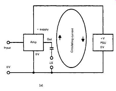
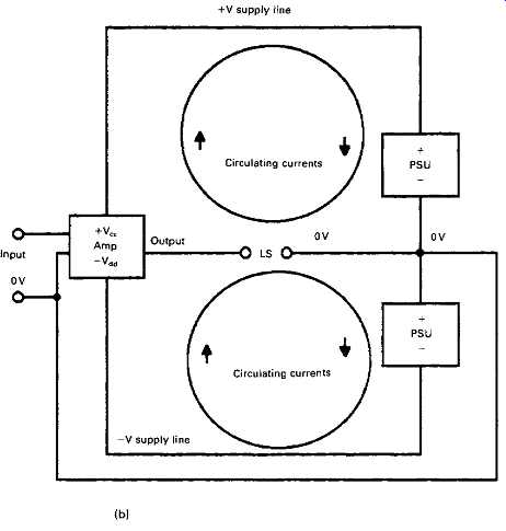
FIG. 1 Amp/PSU current flows, (a) Single-ended system; (b) direct-coupled
system.
CIRCUIT LAYOUTS
The simplest way of converting an input AC voltage waveform of the kind shown in FIG. 2(a) into a DC voltage output is to pass it through some device which will only allow current to flow in one direction (normally called a 'rectifier') as shown in FIG. 2(c). By the choice of a suitable power transformer and rectifier, any required output current or voltage could be obtained. Unfortunately, as illustrated in FIG. 2(b), the output would be a series of uni-directional current pulses. This is satisfactory for operating lamps or motors, perhaps, but not for electronic equipment or audio systems.
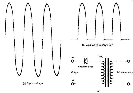
FIG. 2 Simple half-wave rectifier system. (a) Input voltage --- (b) Half-wave
rectification
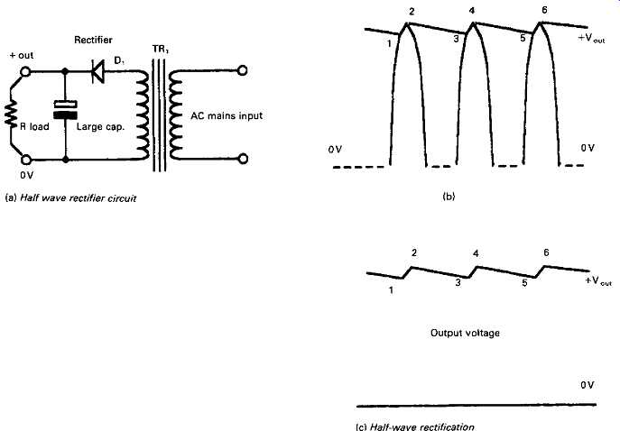
FIG. 3 Half-wave rectifier output ripple. (c) Half-wave rectification (a)
Half wave rectifier circuit (c) Half-wave rectification -- Output voltage
This situation is improved if an output 'reservoir' capacitor is included in the circuit, as shown in FIG. 3(a), to store the output voltage until the following capacitor charging pulse. However, this is still not a complete answer to the design requirement for a smooth, hum-free output voltage, since the voltage stored in this capacitor will decay as current flows through the external load resistor, as shown in FIG. 3(b). The transformer/ rectifier circuit can only recharge this capacitor when the peak transformer output voltage somewhat exceeds the voltage on the capacitor, as is the case between the points labeled 1-2, 3-4, 5-6 and so on. This leaves an undesired ripple on the output DC voltage waveform shown in FIG. 3(c), which worsens , for a given size of reservoir capacitor, as the output current demand is increased.
Unfortunately, this recharging current flows only for a brief period each cycle, and it must be larger than the mean output current by the ratio (cycle duration):(conduction duration). If the reservoir capacitor is large, the rectifier diode has a low conducting resistance, and the transformer is of high quality with a low resistance windings then the peak charging currents when the diode is conducting, between points 1-2, 3-4, etc., will be very high.
CIRCUIT PROBLEMS
No electrical circuit has zero resistance (R) at room temperature, and the voltage (V) developed for a given current flow (I) will be V = IR. In a typical power supply the reservoir capacitor charging currents could well be hundreds of amperes, and this will cause a significant voltage drop, in addition to that due to the circuit resistances, due to the equivalent series resistance (ESR) in the reservoir capacitor. The voltages produced by these pulsating currents will be added to the existing ripple voltage present on the power supply output line.
A further problem of which the power supply unit (PSU) designer must take note is that the very high short-duration circulating currents, during the recharging of the reservoir capacitor, can generate troublesome voltages across all parts of the wiring (or chassis connections) which are in the path from the transformer to the rectifier, to the reservoir capacitor and back to the transformer again. If any part of the signal chain shares any part of this path, it will have some of this 'spiky' short-duration hum voltage added to it. (A further nuisance is that these high peak currents cause strong, short-duration, magnetic fields, which can induce undesired voltages in adjacent wiring.) Unfortunately, all the steps that the designer can take to lessen the ripple on the PSU output, of which the most common is the choice of a very large value, low ESR reservoir capacitor, will tend to make the charging duration shorter and thereby increase the pulsating peak current flow. High pulsating currents also make demands on the construction of the mains transformer - an aspect which I will consider later.
FULL-WAVE RECTIFIER SYSTEMS
An immediate improvement in the performance of any simple transformer/ rectifier system can be made if both halves of the AC output waveform are used, rather than only, say, the positive-going half. This technique, in its various forms, is almost universally employed in PSU systems since it halves the duration of the conducting cycle, and thereby also halves the ripple voltage and the peak reservoir (and transformer secondary) pulse currents.
With valve rectifiers, where it’s necessary to isolate the cathode/heater circuits, the circuit normally used was of the kind shown in FIG. 4(a) for an indirectly heated rectifier valve such as a 5Z4. This kind of valve is to be preferred to a directly heated rectifier, such as the 5U4, if an adequate output current could be obtained, because the HT voltage would only rise gradually following switch-on, as the cathode gradually warmed up to its operating temperature. However, indirectly heated cathodes are less efficient for a given heater wattage, and will have a somewhat shorter operating life.
A fairly common solid-state equivalent system is shown in the circuit of FIG. 4(b). The transformer secondary voltage and ripple waveforms for these types of circuit are shown in Figs 4(c) and 4(d). With solid-state rectifier systems, in which the designer is free from the constraints imposed by the need for heater connections and supplies, other layouts are possible, such as the full-wave bridge rectifier layout shown in FIG. 5(a), used here to provide a single-polarity output voltage. This has an advantage over the layout shown in FIG. 4(b) in that instead of each half of the secondary winding conducting alternately, both secondary windings conduct each half-cycle. This reduces the ratio of peak-to-mean current flow in the transformer secondary circuit, and helps to lessen both the audible hum and the electro-magnetic field radiation from the transformer. However, while this reduces the voltage drop in the secondary windings due to the high peak-current flow, it requires the presence of two rectifier diodes in the path from secondary winding to DC output, instead of just one.
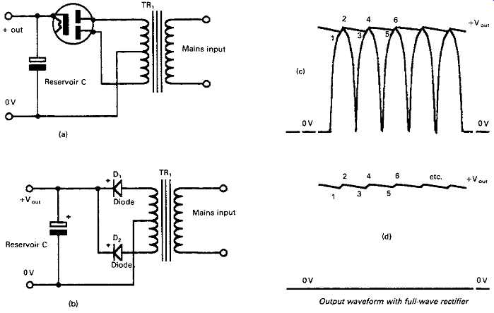
FIG. 4 Full-wave rectifier systems. Output waveform with full-wave rectifier
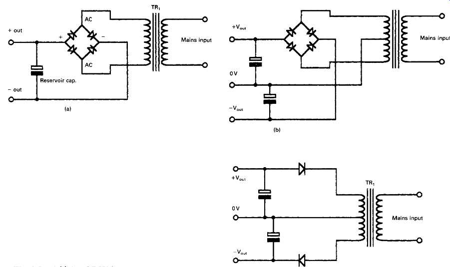
FIG. 5 Additional PSU layouts.
For a twin-polarity power supply output, the most usual circuit layout is that shown in FIG. 5(b), which shares the advantages of more complete utilization of the current output from the secondary winding and also that of lower peak current levels. Both these layouts will give the type of ripple voltage shown in FIG. 4(d). The half-wave rectifier circuit shown in FIG. 5(c) is sometimes found in low-current twin-rail supply systems, where the major considerations are those of simplicity and cheapness. It has the output ripple characteristics shown in FIG. 3(c). The choice of the size of the reservoir capacitor in any of the preceding circuits demands some compromise. The desire to keep the output ripple voltage to the lowest possible level - coupled with the wish, particularly in the case of audio amplifiers, to arrange the PSU so that it can deliver high peak output currents, where required - urges the choice of as large a value of reservoir capacitor as the space and money available will allow.
However, increasing the size of the reservoir capacitor causes the current from the transformer secondary to be drawn in increasingly short pulses, which will worsen the transformer efficiency and heat dissipation. In practice , for any given transformer, the inevitable secondary winding resistance and leakage inductance, associated with core saturation effects, means that there is an optimum reservoir capacitor size, beyond which it’s not useful to go.
TRANSFORMER TYPES AND POWER RATINGS
A major pitfall which lies in wait for the unwary PSU designer is that relating to the maximum output current which may be drawn, without overload, from any circuit with an output reservoir capacitor - such as , for example, those illustrated in Figs 3(a) or 4. The DC output from these layouts will approach that of the peak transformer secondary voltage (approximately 1.4 times the secondary RMS voltage figure, less any voltage drop due to the rectifier or the secondary winding resistance, and less the mean output capacitor voltage droop between recharging cycles). The transformer secondary winding will then be required to deliver a peak current to the reservoir capacitor which is equal, when averaged, to the mean DC drawn from the system. The transformer is then delivering an output power which is equivalent to V peak x 7out rather than VRMS X ???? > and this may be in excess of the manufacturer's rating. A working 'rule of thumb' is that the DC output current (/DC) should not exceed the specified /RMS (max.) x 0.65.
It’s desirable in any mains input transformer that there should be an intimate magnetic coupling between all the windings, and that there should be no stray magnetic field around it. The extent to which this ideal is achieved depends greatly on the nature of the core material (usually grain-oriented silicon steel), and the type of core construction.
In low-cost transformers this core is made by assembling, with the least practicable air gaps in the magnetic circuit, a suitable sized stack of thin, flat, steel alloy 'laminations' - which have been stamped out in the form of 'E's and Ts - within an appropriately shaped hole in an insulating former holding the windings. The laminations must be tightly clamped to prevent core 'buzz', after which the whole assembly will be dipped in some moisture-proofing and insulating lacquer. In higher-quality contemporary transformers the core will be an annular, 0-shaped 'toroid', wound from a continuous thin strip of high-grade magnetic material. The windings are wound around this core by a specially designed machine prior to dipping and impregnation.
Because of the superior magnetic circuit characteristics of the toroidal core, there is much less magnetic field radiation from such a transformer, and it has a superior electrical performance. In high-quality audio equipment these factors will greatly outweigh its less compact construction and its greater cost. Also, because of the way the transformer and its core is made, there is much less core or winding 'buzz' in use - a factor which is welcomed by those with keen ears.
STABILISED PSU CIRCUITS
Low power
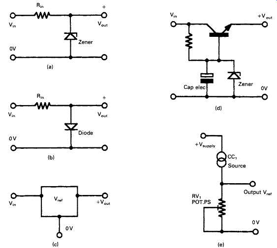
FIG. 6 Voltage reference sources.
There are a number of places in audio amplifier circuitry where a source of some fixed, noise and ripple-free voltage is needed. Some of the circuit layouts used for this purpose are shown in FIG. 6. The most common general-purpose circuit is that using a 'zener' diode, as shown in FIG. 6(a). (The term 'zener' is used loosely to describe all devices of this type, though, strictly, zener diodes are those with output voltages in the range of about 3-5.5 V. Above this voltage they are more properly described as 'avalanche diodes'.) All these reverse-breakdown devices generate a significant amount of electrical noise, and it’s usually prudent to connect a capacitor in parallel with the zener to reduce the noise output as , for example, in FIG. 6(d). If the circuit requires only a relatively low voltage output, a much better circuit, from the point of view of noise, is that of FIG. 6(b), using one or more silicon junction diodes connected in series in the forward (conduction) mode. Multiples of the forward voltage (usually around 0.57-0.6 V) can be obtained in this way. For high-precision, low temperature coefficient applications there is a wide range of voltage 'bandgap' reference sources, such as the ICL8069 or the LM369, which offer very high precision, low-noise, reference sources in the range 1.22-10 V, but these would be rather too expensive for general audio use.
A very simple means of providing a small adjustable reference voltage -- commonly used to generate the forward bias on the output devices in a transistor amplifier - is that shown in FIG. 6(e). The thermal characteristics of the constant current source, CQ, should be chosen to suit the particular application.
Higher power:
Although some manufacturers still prefer to use 'in-house' designs for voltage regulators based on discrete components, the 'three-terminal' voltage regulator ICs of the '78../79..' or '78L../79L..' types have now become an almost inevitable choice for use in relatively low voltage (up to, say, ±24 V) supplies for use with low-level signal circuitry, in preamps or tape/CD/radio systems. The advantages of these ICs are significant. They are cheap, compact, predictable, compensated for variations in ambient temperature, available in both +ve and -ve line versions and have in-built overload protection. They also have a very high degree of power supply ripple rejection, and a low output noise - especially the low-power 'L' series. Although higher-power and higher-voltage versions are becoming increasingly available, they are not, as yet, readily available for use at the voltage, current and power levels needed for audio power amp supplies.
Therefore, in this field, if voltage regulation is required, it will be in the form of a discrete component circuit.
However, the question of whether to use a voltage regulator system opens up philosophical divisions within the audio amp manufacturers, based on their judgment of their likely market. If the power output stage of an audio amplifier is fed directly from a large reservoir capacitor and a massive transformer/rectifier combination, of the general type shown in FIG. 5(b), it will be able to deliver very high powers into the LS load, especially under short-duration signal demands - the origin of the so-called 'music power' ratings of the 1960s. This capability is particularly welcomed by those for whom the physical impact of high-level sound is almost as important as the artistic content of the signal. For those users any regulator circuit which acted to limit the off-load power supply voltage, and the consequent peak sound level output, would be very unwelcome.
Unfortunately, there are also snags. If the power supply can deliver large output currents at high voltages into the LS load, under short-duration music conditions, it will also be able to do it for a longer time under fault conditions, which could be destructive of expensive LS reproducers. The normal type of damage limitation offered by the manufacturers of amps using unprotected PSUs is to incorporate a suitable 'slow-blow' fuse in the output circuit, coupled possibly with some fast-acting overload 'crowbar' circuit to short-circuit the amp output under overvoltage fault conditions.
The snag with the use of any output line fuse is that the integrity of the fuse/fuse-holder contacts will deteriorate with time, and will then introduce unwanted resistance into the LS output circuit.
Some rather less obvious design problems are that the residual (100/ 120 Hz) AC ripple on the PSU output will increase as the output current rises, and this will increase the amplifier background hum level at high output powers. This may not be very noticeable because it will be masked by the music output, but it will be measurable under tests using spectrum analysis, and may be commented upon by suitably equipped reviewers.
An additional problem, more apparent to the designers than to the users, is that the off-load output voltage of such a simple supply system can be up to 40% greater than that on load. This means that components in the power amp will need to support the full off-load voltage, plus some safety margin to allow for mains input voltage surges rather than the supply voltage existing under full-load conditions. These components could be more expensive and, in the particular case of transistors, will usually be of a rather lower electrical performance.
For an audio system which is likely to be used mostly with more traditional music, of which the aesthetic appeal may rely less upon physical impact than upon clarity and tonal purity, a system in which the power amplifier is fed with constant voltage smooth DC supplies, and in which the output power is the same for sustained signal outputs as it’s for brief-duration transients, has much to commend it. However, it may be less well liked by the 'heavy metal' or 'reggae' devotees.
Higher power regulator layouts:
These can be divided into 'shunt' and 'series' connected circuits, of the kinds shown in Figs 6(a) and 6(b) respectively, of which the simple zener diode circuit of Fig. 6(a) is the best-known type. Although zener diodes are available with a range of permissible dissipations from 400 mW to some tens of watts, the higher-power versions are not widely available and expensive. The circuit shown in FIG. 7(a) uses a combination of a power transistor, Q1, with a low-power zener diode to give a high-power shunt regulator circuit. The operating voltage of the zener diode needs to be chosen so that the circuit will draw current from the power supply and reduce its output voltage (due to the voltage drop across its source resistance, Rin), at some point between its off-load and full power voltage levels.
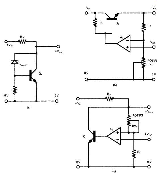
FIG. 7 Shunt and series regulators.
A more elegant circuit arrangement is shown schematically in FIG. 7(c), where the difference between some stable reference voltage and a proportion of the output voltage is amplified and fed to a power transistor connected across the power supply output. The precise operating voltage for this circuit can be chosen by setting the preset potentiometer RVx.
A typical series voltage regulator circuit is shown in FIG. 7(b), in which, once again, a proportion of the PSU output voltage is compared with a reference voltage, and an amplifier, A1, is used to adjust the current fed into the base of the series 'pass' transistor, Ql5 so that the required output voltage is obtained. The snag with a series voltage regulator of this type is that , for correct operation, the input voltage must exceed the required output voltage by some 3 V - known as the 'dropout' voltage - or otherwise the current flow through R1 won’t be adequate to support the required output current.
In the variations of FIG. 7(b) which are available in IC form, the voltage reference is invariably derived from a 'band-gap' type of temperature-compensated voltage source. Not only is the output voltage derived from this arrangement much more stable than that from a zener diode, it’s also much more noise free. This is a point which is sometimes overlooked by designers who use a 'quiet' IC regulator to provide a lower voltage to drive a 'noisy' zener diode.
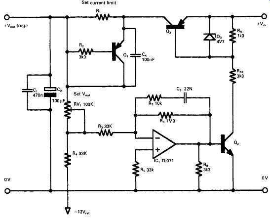
Discrete component voltage regulators can be built to provide any required combination of output voltages and currents, and I am convinced that their use to drive audio amplifier systems does provide worthwhile benefits in sound quality, if for no other reason that such a circuit can have an output impedance which is largely frequency independent and can be less than a tenth of one ohm. To obtain such an output impedance, at, say, 20 Hz from any output capacitor would demand a capacitance value of some 80000 µ¥ - a very bulky and costly alternative. A further advantage of such an electronically controlled supply system is that it can be made to current limit to protect the circuit components from overload, or cut off the supply completely in the event of any amplifier failure. For my own use, I greatly prefer such systems, and described two such layouts for use with power amplifier designs in Electronics + Wireless World (May 1989, pp. 524-527) and Electronics Today (May 1989, pp. 25-33), shown respectively in Figs 8 and 9.
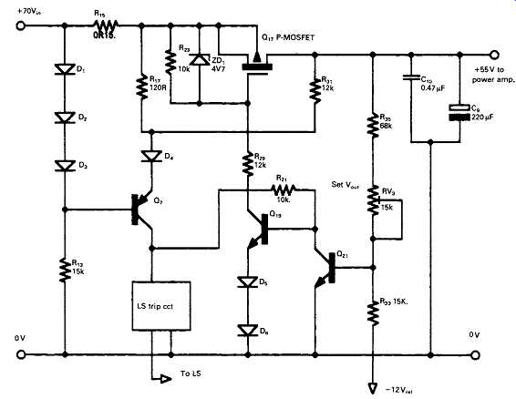
FIG. 9 SIC protected stabilized PSU.
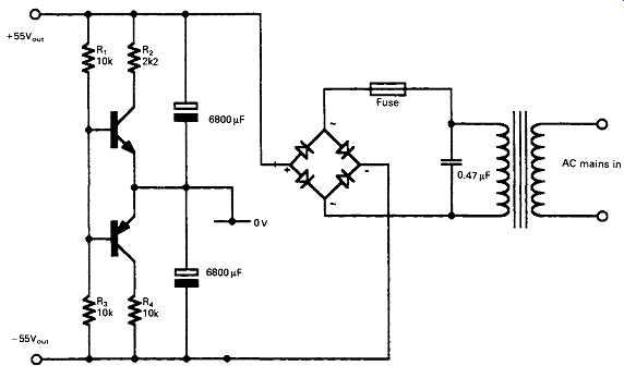
FIG. 10 The Quad power supply system.
COMMERCIAL POWER AMP PSUs
At one time, most of the more highly esteemed audio power amplifiers would have employed some form of PSU output voltage regulation.
However, this approach has now been largely abandoned, I suspect as a result of market pressures, in favor of simpler layouts whose principal feature is an ability to provide the high peak supply line currents needed for some modern music. The PSU circuit details given in the data sheets for the bulk of contemporary power amps show only variations of the simple layout of FIG. 5(b), coupled with some overcurrent protection, or relay switching, circuit to give a measure of LS protection.
Nevertheless, some interesting variations still exist, such as the use by 'Pioneer' of a version of the augmented zener diode layout of FIG. 6(d) as the main power supply line stabilization circuit for their M90(BK) flagship amplifier, an arrangement which is also used by Technics and Rotel. An ingenious system shown in FIG. 10 is used by 'Quad' (the Acoustical Manufacturing Co.) in many of their current power amp designs for converting a single polarity supply into a pair of symmetrical ± voltage lines.
OUTPUT SOURCE IMPEDANCE AND NOISE
Bearing in mind that the output of any amplifier will drive its load in series with its power supply source resistance, and that a proportion of the noise present on the DC power supply lines may also appear on the output signal, the output impedance and noise characteristics of power supply units are of considerable interest to the circuit designer. The commercial three-terminal voltage regulator ICs have a lower noise level and output resistance than small signal zener diodes. They are preferable where these characteristics are important, as , for example, in low-level audio circuitry.
Both primary and secondary cells have good electrical characteristics when new, and the performances of these are listed in Table 9.1.
Table 9.1 Cell and voltage regulator characteristics Notes. The quoted noise levels were measured over a 20 Hz to 20 kHz bandwidth at 20°C. All the (AA size) battery cells had a noise voltage which was below 1 µV on a 10 mA current drain. The '79' series regulators have a somewhat inferior performance by comparison with the '78xx' types. This is because it’s difficult to make good p-n-p transistors in IC form, and this necessitates the use in the *79xx' devices of a somewhat different internal circuit layout.
TRANSFORMER NOISE AND STRAY MAGNETIC FIELDS
All mains transformers generate some audible noise as a result of the alternating magnetic flux and the consequent mutual magnetic repulsion effects within their core and windings, and this can, sometimes, be annoying. E and I type lamination assemblies, used to construct the magnetic cores in conventional low-cost mains transformers, are less good in this respect than the toroidal and 'C-core' constructions used in high-quality equipment. The use of a higher quality core system leads to a much lower external (stray) magnetic field, which facilitates the design of mains-operated units having a low background 'hum' level, and also makes units employing toroidal or similar core transformers less likely to induce mains 'hum' into the circuitry of other units placed in proximity to them.
However, the ability of the core of a transformer to confine the associated magnetic field also depends on the permeability of the core material and this, in turn, depends on the magnitude of the flux within the core. If this approaches saturation the permeability will fall, and the external magnetic field will increase. For this reason the stray magnetic field in proximity to the transformer, as well as its noise level, will increase as the peak currents in its windings increase, and this is a drawback in the use of very large value power supply reservoir capacitors unless this is accompanied by an increase in the power rating of the component.
