SOLID-STATE or semiconductor devices are versatile units that can perform a variety of functions in electronic equipment. Like other electron devices, they have the ability to control almost instantly the movement of charges of electricity. However, in addition, semiconductor devices have many important advantages over other types of electron devices. They are very small and light in weight and have no filaments or heaters; therefore, they require no warm-up time or heating power. Their total power consumption is very low. They are free from micro phonic noise and are rugged because of their solid construction.
SEMICONDUCTOR MATERIALS
Unlike other electron devices, which depend for their functioning on the flow of electric charges through a vacuum or a gas, semiconductor devices make use of the flow of current in a solid. In general, all materials may be classified as conductors, semiconductors, or insulators depending upon their ability to conduct an electric current. As the name implies, a semi conductor material has poorer conductivity (more resistance to current flow) than a conductor, but better conductivity (less resistance to current flow) than an insulator.
The materials most often used in semiconductor devices are germanium and silicon. Germanium is used in many low- and medium-power diodes and transistors. Silicon is more suitable for high-power devices because, among other things, it can be used at much higher temperatures.
The conductivity of semiconductor materials can be increased and con trolled by the addition of small amounts of elements known as "dopants" or "impurities." For example, boron might be used as a dopant for silicon. The use of different types of dopants produces either n-type material, which has excess electrons, or p-type material, which has a shortage of electrons in its crystal structure. A position in the crystal structure from which an electron is missing is called a "hole."
P-N Junctions
When a junction is formed of n-type and p-type materials, as shown in Fig. 1, an interaction takes place in which some of the excess electrons from the n-type material diffuse across the junction and combine with the holes in the p-type material. This interaction creates a small space-charge region (often called the transition region or depletion layer) in the immediate vicinity of the junction. The p-type material in this region acquires a slight negative charge as a result of the addition of electrons; conversely, the n-type material acquires a slight positive charge as a result of the loss of excess electrons.
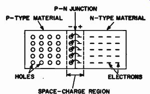
Fig. 1 - Interaction of hole and electrons al p-n junction.
The total effect is that of an imaginary battery connected across the junction having the polarity shown in Fig. 1. In the absence of external circuits and voltages, the voltage difference or potential gradient across the space charge region discourages further dif fusion across the p-n junction and preserves the differences in the characteristics of the two types of materials.
Current Flow
When an external battery is connected across the p-n junction, the amount of current that flows is deter mined by the polarity of the applied voltage and its effect on the space charge region. Fig. 2(a) shows a battery connected to produce reverse bias.
ELECTRON FLOW
(b) FORWARD BIAS
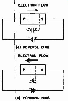
Fig. 2 - Electron current flow in biased p-n junctions.
This connection effectively increases the width of the space-charge region, and the potential gradient increases until it approaches the potential of the external battery; current flow is then extremely small. Under the forward bias condition shown in Fig. 2(b), the space-charge region becomes effectively narrower, and the potential gradient decreases to a very low value; electrons then continue to flow as long as the forward voltage is applied.
The positive to negative current flow defined as conventional current flow is satisfactory for use in circuit analysis. However, in the study of semiconductors, it is helpful to think of current flow in terms of electron flow and "hole" flow. Electron current flows from negative to positive; "hole" current flows from positive to negative.
TYPES OF DEVICES
Silicon Rectifiers Structurally, the silicon rectifier (or semiconductor diode) is a p-n junction; its schematic symbol is shown in Fig. 3.
Rectifiers of this type can be operated at ambient temperatures up to 200°C and at current levels as high as 400 amperes, with voltage levels as high as 1300 volts. Parallel or series arrangements of two or more rectifiers can be used to provide even higher current or voltage capabilities.
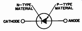
Fig. 3 - Schematic symbol for silicon rectifier. N-TYPE MATERIAL CATHODE P -TYPE
MATERIAL
Because of their high forward-to reverse current ratios, silicon rectifiers can achieve rectification efficiencies greater than 99 percent. When properly used, they have excellent life characteristics that are little affected by aging, moisture, or temperature.
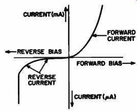
Fig. 4 - Voltage-current characteristics for a silicon rectifier.
They can, however, be easily damaged by sudden rises in junction temperature caused by either surges of high currents or excessive ambient-temperature conditions. They are very small and light-weight, and can be made relatively impervious to shock and other severe environmental conditions.
Fig. 4 shows the voltage-current characteristic for a silicon rectifier under both negative-bias and positive bias conditions. When forward bias is applied (anode positive with respect to cathode), the rectifier behaves very much like a low resistance. The for ward voltage drop Vf (usually about 0.6 volt) is the potential required to overcome the potential gradient of the space-charge region at the p-n junction. This voltage drop remains substantially constant as long as the aver age current in the circuit is within the rated value of the rectifier. However, if the voltage applied to the device is increased (either deliberately or as a result of a voltage surge) to the point where the rated current is appreciably exceeded, the forward voltage drop becomes excessive and the rectifier may be permanently damaged.
Under normal reverse-bias conditions, the rectifier limits current flow to a few microamperes. If the reverse bias exceeds the rated peak reverse voltage (PRY) shown Fig. 4, however, the reverse current increases very rap idly. Any increase in bias beyond the maximum rating may damage the rectifier. More than one diode can be connected in series in a bridge or full wave circuit to obtain the PRY values required for high-voltage power-supply applications.
A zener diode is a special type of diode designed to maintain the voltage constant across a portion of a circuit in spite of relatively large fluctuations in current input to the zener diode.
Bipolar Transistors
A bipolar transistor can be viewed as two diodes (p-n junctions) connected back-to-back, as shown in Fig. 5. The thick end layers are made of the same type of material (n-type in this case), and are separated by a very thin layer ...
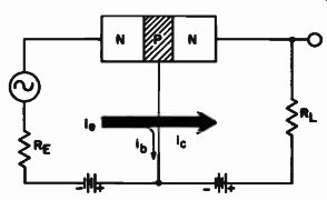
Fig. 5 - N-P-N transistor structure biased for power gain. Arrows denote electron
flow.
... of the opposite type of material (p-type in the device shown). With a battery connected as shown, the p-n junction on the left is positively (forward) biased and conducts current easily (low resistance); the p-n junction on the right is negatively (reverse) biased and impedes current flow (high resistance). Almost all of the current in the for ward-biased junction passes through the thin center region and flows through the reverse-biased junction.
The small remaining current flowing through the base determines the degree of current flow through the reverse biased junction. Because a small amount of current controls a much larger current, a power gain is achieved. This power gain makes the transistor useful as an amplifier and a signal-control (switch) device. (It should be noted that the transistor is a current-amplifying device, rather than a voltage-amplifying device like the vacuum tube.) The schematic symbols for transistors are shown in Fig. 6. The three electrodes of the device are called the emitter (E), the base (B), and the collector (C). In normal operation the emitter to-base junction is biased in the for ward direction and the collector-to base junction in the reverse direction.
The arrow on the emitter lead identifies the transistor as a p-n-p or n-p-n type, and indicates the direction of conventional current flow in a circuit.
P-N-P TRANSISTOR N-P-N TRANSISTOR
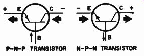
Fig. 6 - Schematic symbols for p-n-p and n p-n transistors. Arrows denote
electron flow.
This arrow always points toward the n type material, and is always in the direction of emitter current flow. The operation of p-n-p devices is similar to that shown in Fig. 5 for the n-p-n device, except that the bias-voltage polarities are reversed, and electron current flow is in the opposite direction.
Transistors can be used in three possible circuit configurations: common-base, common-emitter, and common-collector. Diagrams of these three configurations are shown in Fig. 7. In all three configurations the emitter current is the sum of the base and collector currents. Table 1 lists the properties of the three configurations.
Field-Effect Transistors
Unlike the other transistors described in this book, which are bipolar devices (i.e., performance depends on the interaction of two types of charge carriers, holes and electrons), field-effect transistors are unipolar devices (i.e., operation is a function of only one type of charge carrier, holes in p-channel devices and electrons in n channel devices). The operation of field-effect devices can be explained in terms of a charge control concept. A metal control electrode, which is called a gate, acts as a charge-storage or control element. A charge placed on the gate induces an equal but opposite charge in a semi conductor layer, or channel, located beneath the gate. The charge induced in the channel can then be used to control the conduction between two contacts, called the source and the drain, made to opposite ends of the channel.
In MOS (metal-oxide-semiconductor) field-effect transistors, one or more metal gate electrodes are separated from the semiconductor material by an insulator, as shown in Fig. 8.
These insulated-gate electrodes can deplete the source-to-drain channel of active carriers when suitable bias voltages are applied, or can increase the conductivity of the channel without
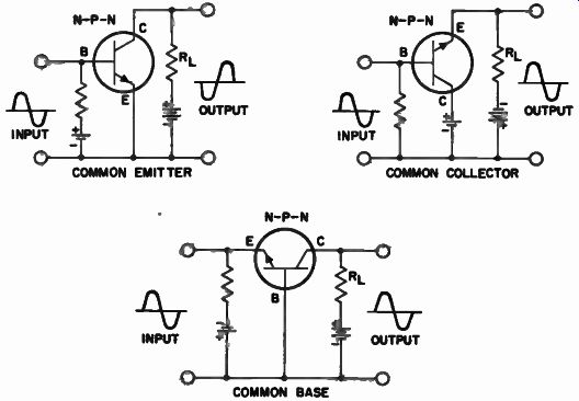
Fig. 7 - Common-emitter, common-collector, and common-base transistor circuit
configurations.
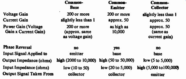
Table 1. Important Properties of the Three Transistor Configurations.
Circuit
increasing steady-state input current or reducing power gain. All MOS field effect transistors used in the circuits in this book are insulated-gate types.
The two basic types of MOS field effect transistors are the depletion type and the enhancement type. In the depletion type, charge carriers are present in the channel when no bias voltage is applied to the gate. A reverse gate voltage is one which depletes this charge and thereby reduces the channel conductivity. A forward gate voltage draws more charge carriers into the channel and thus increases the channel conductivity. In the enhancement type, the gate must be forward-biased to produce the active carriers and permit
SOURCE GATE INSULATION (S102)
DRAIN SUBSTRATE CHANNEL
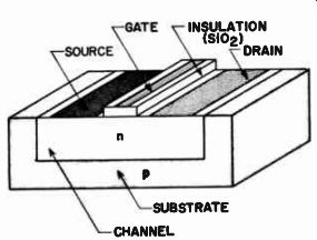
Fig. 8 - Structure of an MOS field-effect transistor.
conduction through the channel. No useful channel conductivity exists at either zero or reverse gate bias. Depletion-type MOS transistors are particularly well suited for use as voltage amplifiers, rf amplifiers, and voltage controlled attenuators. Enhancement type MOS transistors are particularly suitable for switching applications.
Because MOS transistors can be made to utilize either electron conduction (n-channel) or hole conduction (p channel), four distinct types of MOS field-effect transistors are possible. As shown in Fig. 9, the schematic symbol for an MOS transistor indicates whether it is n-channel or p-channel, depletion-type or enhancement-type.
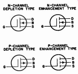
Fig. 9 - Schematic symbols for MOS transistors (G = gate. D = drain, B - active
bulk, S = source). The direction of the arrowhead in the symbol identifies
the n-channel device (arrow pointing toward the channel) or the p-channel device
(arrow pointing away from the channel). The channel line itself is made solid
to identify the "normally ON" depletion type, or is interrupted to
identify the "normally OFF" enhancement type.
Dual-gate MOS field-effect transistors have two independent insulated gates. The dual-gate transistors exhibit all the features of single-gate field effect transistors, but perform better in certain applications.
Fig. 10 shows a schematic representation of a dual-gate MOS field-effect transistor. The transistor includes three diffused regions connected by two channels, each of which is con trolled by its own independent gate.
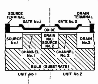
Fig. 10 - Schematic representation of a dual-gate MOS field effect transistor.
Unit No. 1 acts as a conventional single-gate MOS field-effect transistor, with the central diffused region acting as the drain and unit No. 2 acting as a load resistor. Similarly, unit No. 2 can be used as an independent triode with unit No. 1 acting as a source resistor. Fig. 11 shows these configurations from a circuit view point, together with the circuit symbol for the dual-gate unit.
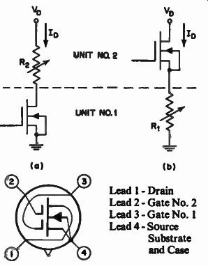
Fig. 11 - Equivalent circuit representation of the two units in a dual-gate
MOS transistor and the terminal diagram for the transistor.
A dual-gate MOS transistor can be cut off if either gate is made sufficiently negative with respect to the source. When one gate is biased to cutoff, a change in the voltage on the other gate is equivalent to a change in the value of a resistance in series with a cut-off transistor.
Thyristors
The term thyristor is the generic name for semiconductor devices that have characteristics similar to those of thyratron tubes. Basically, this group includes bistable semiconductor devices that have three or more junctions (i.e., four or more semiconductor layers) and that can be switched between conducting states (from OFF to ON or from ON to OFF). The two most popular types of thyristors are the silicon controlled rectifier (SCR) and the triac.
A silicon controlled rectifier (SCR) is basically a four-layer p-n-p-n device that has three electrodes (a cathode, an anode, and a control electrode called the gate). Fig. 12 shows the junction diagram, principal voltage-current characteristic, and schematic symbol for an SCR. A triac also has three electrodes (main terminal No. 1, main terminal No. 2, and gate) and may be considered as two parallel p-n-p-n structures oriented in opposite directions to provide symmetrical bidirectional electrical characteristics. Fig. 13 shows the junction diagram, voltage current characteristic, and schematic symbol for a triac.
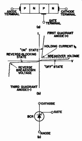
Fig. 12 - Junction diagram (a), principal voltage-current characteristic (b),
and schematic symbol (c)for an SCR thyristor.
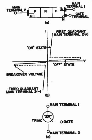
Fig. 13 - Junction diagram (a). principal voltage-current characteristic (
b). and schematic (c)for a triac thyristor.
Fig. 12(b) shows that under reverse bias conditions (anode negative with respect to cathode) the SCR has a very high internal impedance, and only a slight amount of reverse current, called the reverse blocking current, flows through the p-n-p-n structure. This current is very small until the reverse voltage exceeds the reverse breakdown voltage; beyond this point, however, the reverse current increases rapidly.
The value of the reverse breakdown voltage differs for individual SCR types.
During forward-bias operation (anode positive with respect to cathode), the p-n-p-n structure of the SCR is electrically bistable and may exhibit either a very high impedance (forward blocking or OFF state) or a very low impedance (forward-conducting or ON state). In the forward-blocking state, a small forward current, called the for ward OFF-state current, flows through the SCR. The magnitude of this current is approximately the same as that of the reverse-blocking current that flows under reverse-bias conditions. As the forward bias is increased, a voltage point is reached at which the forward current increases rapidly, and the SCR switches to the ON state. This value of voltage is called the forward breakover voltage.
When the forward voltage exceeds the breakover value, the voltage drop across the SCR abruptly decreases to a very low value, referred to as the for ward ON state voltage. When an SCR is in the ON state, the forward current is limited primarily by the impedance of the external circuit. Increases in forward current are accompanied by only slight increases in forward voltage when the SCR is in the state of high forward conduction.
An important feature of the SCR is its low power loss as compared with the amount of power it controls. For example, an SCR can control as much as 350 watts with a maximum power loss of less than two watts (3.2 max amperes x 0.6 volt), an insignificant amount compared to the power loss in a rheostat required to control the same amount of power.
As shown in Fig. 13 (b), a triac exhibits the forward-blocking, for ward-conducting voltage-current characteristic of a p-n-p-n structure for either direction of applied voltage. This bidirectional switching capability results because, as mentioned previously, a triac consists essentially of two p-n-p-n devices of opposite orientation built into the same crystal.
The device, therefore, operates basically as two SCR's connected in parallel, but with the anode and cathode of one SCR connected to the cathode and anode, respectively, of the other SCR. As a result, the operating characteristics of the triac in the first and third quadrants of the voltage current characteristics are the same, except for the direction of current flow and applied voltage. The triac characteristics in these quadrants are essentially identical to those of an SCR operated in the first quadrant. For the triac, however, the high-impedance state in the third quadrant is referred to as the OFF state rather than as the reverse-blocking state. Because of the symmetrical construction of the triac, the terms forward and reverse are not used in reference to this device.
Thyristors are ideal for switching applications. When the working voltage of a thyristor is below the break over point, the current through the device is extremely small and the thyristor is effectively an open switch.
When the voltage across the main terminals increases to a value exceeding the breakover point, the thyristor switches to its high-conduction state and is effectively a closed switch. The thyristor remains in the ON state until the current through the main terminals drops below a value which is called the holding current. When the source voltage of the main-terminal circuit can not support a current equal to the holding current, the thyristor reverts back to the high-impedance OFF state.
The breakover voltage of a thyristor can be varied, or controlled, by injection of a signal at the gate, as indicated by the family of curves shown in Fig. 14. Although this family of curves is shown in the first quadrant and is typical of SCR operation, a similar set of curves can also be drawn for the third quadrant to represent triac operation.
When the gate current is zero, the principal voltage must reach the breakover value V (Bo) of the device before break over occurs. As the gate current is increased, however, the value of break over voltage becomes less until the ...
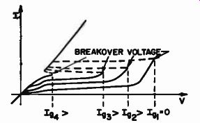
Fig. 14 - Curves showing breakover characteristics of a thyristor for different
values of gate current.
... curve closely resembles that of a rectifier. In normal operation, thyristors are operated with critical values well below the breakover voltage and are made to switch ON by gate signals of sufficient amplitude to assure that the device is switched to the ON state at the instant desired.
After the thyristor is triggered by the gate signal, the current through the device is independent of gate voltage or gate current. The thyristor remains in the ON state until the principal current is reduced to a level below that required to sustain conduction.
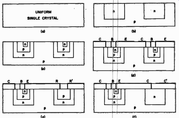
Fig. 15 - Basic steps in integrated-circuit production using the silicon process:
(a) silicon wafer used as starting material for an integrated circuit; (b)
diffusion of n-type areas to provide isolated circuit nodes; (c) diffusion
of additional p-type and n-type regions to form transistors; (d) addition of
metallized contacts to transistor elements; (e) connection of contacts to p-type
region to form integrated resistor; (f use of oxide as a dielectric to form
integrated capacitor.
Integrated Circuits
The fundamental requirement of an integrated circuit is that components be processed simultaneously from common materials. A variety of technologies can be used to satisfy this requirement. The technology presently used is based on the silicon planar technology developed for transistors.
The basic steps of the silicon process are shown in Fig. 15. The starting material is a uniform single crystal of p-type silicon called the chip. Successive diffusion processing steps permit the introduction of impurities to desired depths and widths in the starting material to form transistors, resistors, and capacitors. Vertical penetration of the impurities is controlled by the diffusion temperature and time, and lateral control of the diffusions is made possible by combination of the masking properties of silicon dioxide with photo-chemical techniques. The silicon wafer is then coated with an insulating oxide layer, and the oxide is opened selectively to permit metallization and interconnection.
Fig. 16 shows the combination of the three types of elements on a single wafer, together with the equivalent circuit. Fig. 17 shows an enlargement of a completed integrated circuit, the CA3020, together with the corresponding circuit diagram. The callouts on the photograph denote the location of the components shown in the circuit diagram. The actual chip is about 1/4 the size of terminal 4 as shown in the photograph.
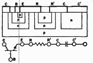
Fig. 16 - Completed silicon chip containing transistor, resistor, and capacitor.
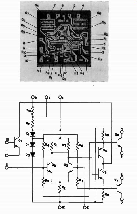
Fig. 17 - Metallization pattern, component location, and circuit diagram for
the CA 3020 integrated circuit.
Because the basic fabrication process for integrated circuits is almost identical with that used to fabricate transistors, transistors formed by this technology are similar to discrete units. Integrated resistors, however, are significantly different from conventional, discrete versions. Discrete resistors are normally made in standard sizes, and different values are obtained by variations in the resistivity of the material. In integrated circuits, the by the optimum value required for the resistivity of the material is determined transistor base diffusion and cannot be varied to provide different resistance values. Therefore, the value of the resistor depends primarily on the ratio of its length to its width: high-valued resistors are long and narrow and low valued resistors are short but wide.
The value of an integrated capacitor depends on its area, its dielectric constant, and the thickness of the oxide layer. Because the oxide thickness is kept constant, capacitor values vary directly with area.
SENSORS
Photocells
Fig. 18 shows a typical photoconductive cell, a 1/4-inch-diameter broad-area cadmium-sulfide device.
Photocells of this type, which are also known as photoresistors or light dependent resistors, have a polycrystalline photosensitive surface and are characterized by high sensitivity to visible radiation and moderate speed of response to changes in illumination.
The resistance of the cell decreases as the illumination level increases, as shown in Fig. 19
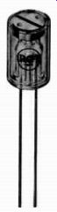
Fig. 18 - Photoconductive cell contained in RCA Add-On Light-Sensor Experimenter's
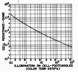
Fig. 19 - Resistance of photocell KD2106 as a function of illumination.
Thermistors
A thermistor is a solid-state device that has a very large, controlled, negative or positive resistance-temperature characteristic. This unique characteristic makes thermistors very useful for applications which interrelate thermal data. Fig. 20 shows resistance-temperature characteristics for three thermistors which have a negative temperature coefficient (i.e., resistance decreases with increasing temperature).
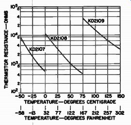
Fig. 20 - Resistance-temperature characteristics of thermistors contained
in RCA Add-On Heat-Sensor Experimenter's Kit KD2110.
++++++++++++