THE CIRCUITS described in this chapter are the basic elements of some of a great many electronic circuits in common use. They represent some of the "building blocks" or foundations on which the majority of circuits in this book are constructed. An understanding of the functioning of these fundamental circuits will be of great help in understanding the operation of the practical circuits presented later. The simplified diagrams in this chapter show only the basic configuration for each circuit; component values and construction information are given with the complete practical circuit.
AMPLIFIERS
There are many different types of amplifiers; the type used in any given circuit depends on the application for which the circuit is intended. Power output, load, signal characteristics, and cost are but a few of the many factors that must be considered before an amplifier can be chosen for a particular job.
The circuit in Fig. 21 shows a very basic amplifier; a circuit in which a small current controls a much larger current. Resistor R1 is the bias resistor; R2 is the collector load resistor; and capacitor C1 blocks dc from the output.
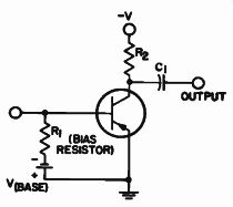
Fig. 21 - A basic transistor amplifier.
The battery voltage establishes, through R1 , a small current in the base emitter junction of the transistor. This current is a steady-state current; that is, it flows all the time. The small base emitter current establishes a much greater current in the collector-emitter junction. The larger current is con trolled or voltage-variable resistors of the transistor; the large signal output of the amplifier, therefore, varies with the small input signal.
Additional parts may be added to this basic configuration to improve such qualities as stability and fidelity; however, the principle of operation remains the same.
Voltage Variable Resistor (VVR)
Because the drain-current/ drain-voltage characteristic of MOS transistors remains linear at low drain to-source voltages, the devices can be used as low-distortion voltage-con trolled or voltage-variable resistors (VVR's). The principal advantages of MOS transistors in this application are negligible gate-power requirements and large dynamic range. Fig. 22 shows a voltage-variable resistor circuit using an MOS transistor.
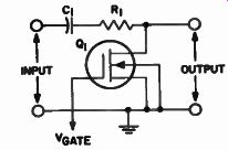
Fig. 22 - A voltage-variable resistor circuit using an MOS transistor.
Series Regulator
A series regulator circuit is essentially a direct-coupled amplifier that is used to amplify an error or difference signal obtained from a comparison between a portion of the output voltage and a reference source. Series regulators maintain a constant voltage output and are used in regulated power supplies. Fig. 23 shows the circuit of a typical series regulator. The reference-voltage source VR is placed in the ...
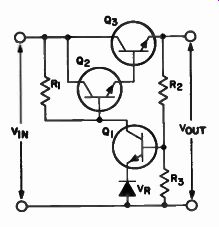
Fig. 23 - A typical series
regulator circuit.
... emitter circuit of the amplifier transistor Q1 so that the error or difference signal between VR and some portion of the output voltage V.., is developed and amplified. The amplified error signal forms the input to the regulating element consisting of transistors Q2 and Q3 ; the output from the regulating element develops a controlling voltage across the resistor R1.
Shunt Regulator
Shunt regulator circuits are not as efficient as series regulator circuits for most applications, but they have the advantage of greater simplicity. In the shunt voltage regulator circuit in Fig. 24, the current through the shunt element consisting of transistors Q1 and Q2 varies with changes in the load current or input voltage. This current variation is reflected across the resistance R1 in series with the load so that the output voltage V., is maintained nearly constant. Transistor Q1, the shunt element, must be capable of absorbing all power input to the circuit by the supply when load current is very low.
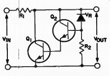
Fig. 24 - A typical shunt regulator circuit.
OSCILLATORS
An oscillator circuit is similar in many respects to an amplifier, except that a portion of the output power is returned to the input network in phase with the starting power (positive or regenerative feedback) to provide a self-generating or self-repeating current or voltage variation at a definite rate. Oscillators can be made to produce many different waveshapes; the two oscillators described below generate sine waves.
Fig. 25(a) is a transistor version of the Colpitts oscillator. Positive feed back is obtained from the voltage-divider circuit consisting of capacitors C2 and C3 in parallel with the primary winding of the transformer. The voltage developed across C3 is the feed back voltage and is applied to the emit ter of the transistor. The frequency and the amount of feedback voltage can be controlled by adjustment of either or both capacitors. For minimum feed back loss, the ratio of the capacitive reactance between C2 and C3 should be approximately equal to the ratio between the output impedance and the input impedance of the transistor. Base bias is provided by resistors R2 and R3; R4 is the collector load resistor. R1 develops the emitter input signal and acts as the emitter stabilizing resistor.
Fig. 25(b) and 25(c) show the MOS field-effect transistor in use in two forms of the Colpitts oscillator circuit.
These circuits are commonly used in vhf and uhf equipment. Feedback in the MOS-transistor Colpitts oscillator is controlled by the ratio of C2 to C3. Improved circuit stability is supplied by diode D1 in Fig. 25(c); the diode provides automatic amplitude control and maintains voltage swings within the capability of the MOS transistor.
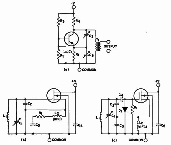
Fig. 25 - Colpitts oscillator circuits: (a) is a bipolar-transistor version,
(b) and (c) are MOS field-effect transistor versions.
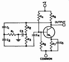
Fig. 26 - A basic twin-T bridge oscillator.
BASIC TWIN-T BRIDGE OSCILLATOR
The circuit in Fig. 26 represents a basic twin-T bridge oscillator. The oscillator takes its name from the frequency-determining and dc-blocking COMMON
RC network in the left-hand part of the circuit (C1, C2, C3, R1, R2 , R3 ). Resistors R4, RS, R6, and R7 provide the necessary bias conditions for the transistors. Resistor R7 is the emitter-stabilizing resistor; CS , RS , and R7 along with the transistor comprise the transistor amplifier. Capacitor C4 couples the oscillator signal to the base of the transistor and also blocks dc. Capacitor C5 bypasses ac signals and prevents degeneration.
SWITCHES
Astable and Monostable Pulsers or Clock Circuits
Astable (free-running) pulsers are oscillators used to generate pulses at specific frequencies in such applications as light flashers, pulse generators, and clock-pulse sources. Monostable ("one-shot") pulsers are used principally for pulse shaping and as time delay circuits.
The basic astable pulser circuit is shown in Fig. 27. Transistors Q1 and Q2 form a regenerative switch. This switch has a very high impedance until it is triggered into conduction; after triggering it has a very low impedance.
When power is applied to the circuit, capacitor C2 charges through the emitter of Q1, turning it on and causing the regenerative switch to conduct.
COMMON
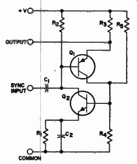
Fig. 27 - The basic astable pulser or clock circuit.
When capacitor C2 charges, the emitter of Q2 becomes more negative and turns the regenerative switch off.
The high impedance of the switch in the OFF condition causes C2 to discharge through R1. As the charge on C2 decreases, the emitter of Q2 becomes less negative and the switch begins to conduct again. This process is repeated as long as power is applied to the circuit.
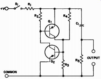
Fig. 28 - The basic monostable pulser or clock circuit.
The basic monostable clock or pulser is shown in Fig. 28. Transistors Q1 and Q2 form a regenerative switch similar to the one described above for the astable pulser. When switch S1 is closed, a voltage is applied across R5 and the output terminals, and capacitor C1 , starts to charge. When the voltage across C1 and R5 together reaches the triggering level of the regenerative switch (which is in parallel with C1 and Rs), conduction through the switch occurs. C1 then discharges through R5 and the regenerative switch. The re generative switch stays in the conductive state as long as S1 is closed.
Because the voltage across the con ducting regenerative switch is very low and because the regenerative switch is in parallel with the C1 R5 combination, the output voltage is also very low. The circuit will remain in the state described until S1 is re-operated.
Multivibrator (Astable)
Oscillator circuits that produce nonsinusoidal output waveforms can use a regenerative circuit in conjunction with resistance-capacitance (RC) or resistance-inductance (RL) components to produce a switching action.
The charge and discharge times of the reactive elements are used to produce sawtooth, square, or pulse output waveforms.
A multivibrator is essentially a nonsinusoidal two-stage oscillator in which one stage conducts while the other is cut off until a point is reached at which the conditions of the stages are reversed. This type of oscillator is normally used to produce a square wave output. In the RC-coupled common-emitter multivibrator shown in Fig. 29, the output of transistor Q2 is coupled to the input transistor Q2 through the feedback capacitor C1 , and the output of Q2 is coupled to the input of Q1 through the feedback capacitor C2 .
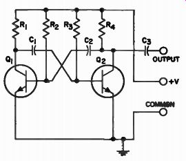
Fig. 29 -An RC-coupled common-emitter multivibrator.
In the multivibrator circuit, an increase in the collector current of transistor Q1 causes a decrease in the collector voltage which, when coupled through capacitor C1 to the base of transistor Q2 , causes a decrease in the collector current of Q2 . The resultant rising voltage at the collector of Q2, when coupled through capacitor C2 to the base of Q1, drives Q1 further into conduction. This regenerative process occurs rapidly, driving Q1 into heavy saturation and Q2 into cutoff. Q2 is maintained in a cutoff condition by C1 (which has previously charged to the supply voltage through resistor RI) until C1 discharges through R3 toward the collector-supply potential. When the junction of C1 and R3 reaches a slight positive voltage, however, transistor Q2 begins to conduct and the regenerative process reverses. Q2 then reaches a saturation condition, Q1 is cut off by the reverse bias applied to its base through C2 , and the C2 R2 junction starts charging toward the collector supply voltage. The oscillating frequency of the multivibrator is deter mined by the values of resistance and capacitance in the circuit.
Basic Digital Flip-Flop
The basic digital flip-flop circuit is shown in Fig. 30. The resistor and bias values of this circuit are chosen so that the initial application of dc power causes one transistor to be cut off and the other to be driven into saturation.
Because of the feedback arrangement, each transistor is held in its original state by the condition of the other. The application of a positive trigger pulse to the base of the OFF transistor or a negative pulse to the base of the ON transistor switches the conducting state of the circuit. The new state is then maintained until a second pulse triggers the circuit back to the original state.
In Fig. 30, two separate inputs are shown. A trigger pulse at input A will change the state of the circuit. An input of the same polarity at input B or an input of opposite polarity at input A will then return the circuit to its original state. (Collector triggering can be accomplished in a similar manner.) Capacitors C3 and C4 are used to speed up the regenerative switching action.
The output of the circuit is a unit step voltage when one trigger is applied, or a square wave when continuous pulsing of the input is used.
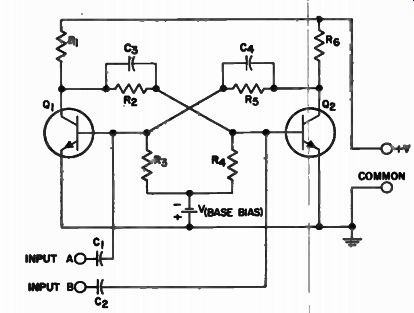
Fig. 30 - A basic digital flip-flop.
NAND Gate
A NAND gate such as that shown in Fig. 31 provides an output when all inputs are applied simultaneously.
When a positive input pulse is applied to only one of the transistors in the NAND gate, that transistor turns on; however, conduction cannot occur because the ON transistor is in series with another transistor that is turned off. When positive pulses are applied to both inputs simultaneously, conduction does occur and a negative output is produced. In a NAND gate the polarity of the output is opposed to that of the input; in an AND gate, input and output polarities are the same.
OUTPUT
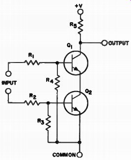
Fig. 31 - A basic NAND gate.
NOR Gate The circuits in Figs. 32 and 33 are NOR gates. A NOR gate circuit consists basically of a transistor that is held in the OFF state. A positive signal on any of the inputs large enough to turn the transistor on causes the output to go negative or to substantially ground potential. When the output ...
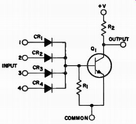
Fig. 32 - A positive-action diode-transistor NOR gate.
... polarity is opposite to the input polarity the circuit is a NOR gate; when input and output polarities are identical, the circuit is called an OR gate.
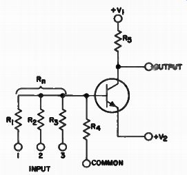
Fig. 33. A positive-action resistor- transistor NOR gate.
The use of a diode in the positive action diode-transistor NOR gate shown in Fig. 32 eliminates some of the losses associated with resistive input circuits and thereby increases the number of possible outputs for a given transistor and switching speed. The diode does not conduct any appreciable current when the input is low. The diode has a high stored charge when forward-biased; when the transistor is turned off, therefore, the stored charge of the diode compensates that of the transistor.
In a positive-action gate there are only two states, on and off; there is no state in which a limited amount of conduction takes place.
INDICATOR-LAMP CIRCUIT
A positive signal applied to the base of Q1 in Fig. 34 turns Q1 on and permits current to flow through R2 and R3. Because R2 is in parallel with the base-emitter junction of Qz , the current passing through it puts a forward bias on Q2 and causes it to turn on. Conduction through Q2 lights the lamp, I_1.
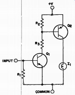
Fig.
34 - An indicator-lamp driver circuit.
++++++++++++