(cont. from part 1)
Automatic Volume or Gain Control
The chief purpose of automatic volume control (avc) or automatic gain control (age) in a radio or television receiver is to prevent fluctuations in loudspeaker volume or picture bright ness when the audio or video signal at the antenna is fading in and out.
An automatic volume control circuit regulates the receiver rf and if gain so that this gain is less for a strong signal than for a weak signal. In this way, when the signal strength at the antenna changes, the avc circuit reduces the resultant change in the voltage output of the last if stage and consequently reduces the change in the speaker output volume.
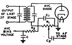
Fig. 61-Automatic-volume-control (avc) circuit.
The avc circuit reduces the rf and if gain for a strong signal usually by in creasing the negative bias of the rf, if, and frequency-mixer stage when the signal increases. A simple avc circuit is shown in Fig. 61. On each positive half cycle of the signal voltage, when the diode plate is positive with respect to the cathode, the diode passes current.
Because of the flow of diode current through R1, there is a voltage drop across R1 which makes the left end of R1 negative with respect to ground. This voltage drop across Ri is applied, through the filter R, and C, as negative bias on the grids of the preceding stages.
When the signal strength at the antenna increases, therefore, the signal applied to the avc diode increases, the voltage drop across R1 increases, the negative bias voltage applied to the rf and if stages increases, and the gain of the rf and if stages is decreased. Thus the increase in signal strength at the antenna does not produce as much increase in the output of the last if stage as it would produce without avc.
When the signal strength at the antenna decreases from a previous steady value, the avc circuit acts, of course, in the reverse direction, applying less negative bias, permitting the rf and if gain to increase, and thus reducing the decrease in the signal output of the last if stage. In this way, when the signal strength at the antenna changes, the avc circuit acts to reduce change in the output of the last if stage, and thus acts to reduce change in loudspeaker volume.
The filter, C and Ra, prevents the avc voltage from varying at audio frequency. The filter is necessary because the voltage drop across R1 varies with the modulation of the carrier being received. If avc voltage were taken directly from R1 without filtering, the audio variations in avc voltage would vary the receiver gain so as to smooth out the modulation of the carrier. To avoid this effect, the avc voltage is taken from the capacitor C. Because of the resistance R3 in series with C, the capacitor C can charge and discharge at only a comparatively slow rate. The avc voltage therefore cannot vary at frequencies as high as the audio range but can vary at frequencies high enough to compensate for most fading. Thus the filter permits the avc circuit to smooth out variations in signal due to fading, but prevents the circuit from smoothing out audio modulation.
It will be seen that an avc circuit and a diode-detector circuit are much alike. It is therefore convenient in a receiver to combine the detector and the avc diode in a single stage. Examples of how these functions are combined in receivers are shown in Circuits section.
In the circuit shown in Fig. 61, a certain amount of avc negative bias is applied to the preceding stages on a weak signal. Because it may be desirable to maintain the receiver rf and if gain at the maximum possible value for a weak signal, avc circuits are designed in some cases to apply no avc bias until the signal strength exceeds a certain value. These avc circuits are known as delayed avc or davc circuits.
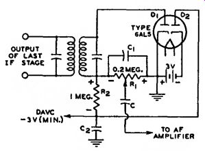
Fig. 62-Delayed avc (davc) circuit.
A davc circuit is shown in Fig. 62.
In this circuit, the diode section D, of the 6AL5 acts as detector and avc diode.
Rt is the diode load resistor and R2 and C2 are the avc filter. Because the cathode of diode D2 is returned through a fixed supply of -3 volts to the cathode of D1, a dc current flows through R, and R2 in series with D,.. The voltage drop caused by this current places the avc lead at approximately -3 volts (less the negligible drop through D2). When the average amplitude of the rectified signal developed across Rt docs not exceed 3 volts, the avc lead remains at -3 volts. Hence, for signals not strong enough to develop 3 volts across R,. the bias applied to the controlled tubes stays constant at a value giving high sensitivity.
However, when the average amplitude of rectified signal voltage across R1 exceeds 3 volts, the plate of diode Da becomes more negative than the cathode of D2 and current flow in diode D2 ceases. The potential of the avc lead is then controlled by the voltage developed across R1. Therefore, with further increase in signal strength, the avc circuit applies an increasing avc bias voltage to the controlled stages. In this way, the circuit regulates the receiver gain for strong signals, but permits the gain to stay constant at a maximum value for weak signals.
It can be seen in Fig. 62 that a portion of the -3 volts delay voltage is applied to the plate of the detector diode D1, this portion being approximately equal to Ri/(Ri + Rj) times -3 volts. Hence, with the circuit constants as shown, the detector plate is made negative with respect to its cathode by approximately one-half volt. However, this voltage does not interfere with detection because it is not large enough to prevent current flow in the tube.
Automatic gain control (age) compensates for fluctuations in rf picture carrier amplitude. The peak carrier level rather than the average carrier level is controlled by the age voltage because the peaks of the sync pulses are fixed when inserted on a fixed carrier level.
The peak carrier level may be determined by measurement of the peaks of the sync pulses at the output of the video detector.
A conventional age circuit, such as that shown in Fig. 63, consists of a diode detector circuit and an RC filter. The time constant of the detector circuit is made large enough to prevent the picture content from influencing the magnitude of the age voltage. The output voltage (age voltage) is equal to the peak value of the incoming signal.
The diode detector receives the in coming signal from the last if stage of the television receiver through the capacitor C1. The resistor R1 provides the load for the diode. The diode conducts only when its plate is driven positive with respect to its cathode. Electrons then flow from the cathode to the plate and thence into capacitor C1, where the negative charge is stored. Because of the low impedance offered by the diode during conduction, G charges up to the value of the peak applied voltage.
During the negative excursion of the signal, the diode does not conduct, and C1 discharges through resistor R1.
Because of the large time constant of R1C1, however, only a small percentage of the voltage across G is lost during the interval between horizontal sync pulses. During succeeding positive cycles, the incoming signal must over come the negative charge stored in G before the diode conducts, and plate current flows only at the peak of each positive cycle. The voltage across G, therefore, is determined by the level of the peaks of the positive cycles, or the sync pulses.
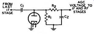
Fig. 63-Automatic-gain control (age) circuit.
The negative voltage developed across resistor Ri by the sync pulses is filtered by resistor R. and capacitor Ct to remove the 15,750-cycle ripple of the horizontal sync pulse. The dc output is then fed to the if and rf amplifiers as an age voltage.
This age system may be expanded to include amplification of the age signal before detection of the peak level, or amplification of the dc output, or both.
A direct-coupled amplifier must be used for amplification of the dc signal. The addition of amplification makes the system more sensitive to changes in carrier level.
A "keyed" age system such as that shown in Fig. 64 is used to eliminate flutter and to improve noise immunity in weak signal areas. This system provides more rapid action than the conventional age circuits because the filter circuit can employ lower capacitance and resistance values.
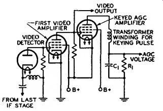
Fig. 64-"Keyed" age circuit.
In the keyed age system, the negative output of the video detector is fed directly to the grid No. 1 of the first video amplifier. The positive output of the video amplifier is, in turn, fed directly to the grid No. 1 of the keyed age amplifier. The video stage increases the gain of the age system and, in addition, provides noise clipping. The plate voltage for the age amplifier is a positive pulse obtained from a small winding on the horizontal output transformer which is in phase with the horizontal sync pulse obtained from the video amplifier.
The polarity of this pulse is such that the plate of the age amplifier tube is positive during the retrace time. The tube is biased so that current flows only when the grid No. 1 and the plate are driven positive simultaneously. The amount of current flow depends on the grid-No. 1 potential during the pulse.
These pulses are smoothed out in the RC network in the plate circuit (Rid).
Because the dc voltage developed across R1 is negative, it is suitable for application to the grids of the rf and if tubes as an age voltage.
High-Fidelity Amplifiers
Several high-fidelity amplifiers are shown in the Circuits section. The performance capabilities of such amplifiers are usually given in terms of frequency response, total harmonic distortion, maximum power output, and noise level.
To provide high-fidelity reproduction of audio program material, an amplifier should have a frequency response which does not vary more than 1 dB over the entire audio spectrum. General practice is to design the amplifier so that its frequency response is flat within 1 dB from a frequency below the lowest to be reproduced to one well above the upper limit of the audible region.
Harmonic distortion and inter modulation distortion produce changes in program material which may have adverse effects on the quality of the reproduced sound. Harmonic distortion causes a change in the character of an individual tone by the introduction of harmonics which were not originally present in the program material. For high-fidelity reproduction, total harmonic distortion (expressed as a percentage of the output power) should not be greater than about 1 percent at the desired listening level. Types such as the 6973, 7027A and 7868 are designed to provide extremely low harmonic distortion in suitably designed push-pull amplifier circuits.
Intel-modulation distortion is a change in the waveform of an individual tone as a result of interaction with an other tone present at the same time in the program material. This type of distortion not only alters the character of the modulated tone, but may also result in the generation of spurious signals at frequencies equal to the sum and difference of the interacting frequencies.
Intermodulation distortion should be less than 2 percent at the desired listening level. In general, any amplifier which has low intermodulation distortion will have very low harmonic distortion.
The maximum power output which a high-fidelity amplifier should deliver depends upon a complex relation of several factors, including the size and acoustical characteristics of the listening area, the desired listening level, and the efficiency of the loudspeaker system. Practically, however, it is possible to determine amplifier requirements in terms of room size and loudspeaker efficiency.
The acoustic power required to reproduce the loudest passages of orchestral music at concert-hall level in the average-size living room is about 0.4 watt. Because high-fidelity loudspeakers of the type generally available for home use have an efficiency of only about 5 percent, the output stage of the amplifier should therefore be able to deliver a power output of at least 8 watts. Be cause many wide-range loudspeaker systems, particularly those using frequency divider networks, have efficiencies of less than 5 percent, output tubes used with such systems must have correspondingly larger power outputs. The 6973, 7027A, 7189, and 7868 can provide ample output for most systems when used in suitable push-pull circuits.
The noise level of a high-fidelity amplifier determines the range of volume the amplifier is able to reproduce, i.e., the difference (usually expressed in decibels) between the loudest and softest sounds in program material.
Because the greatest volume range utilized in electrical program material at the present time is about 60 dB, the noise level of a high-fidelity amplifier should be at least 60 dB below the signal level at the desired listening level.
Limiters
An amplifier may also be used as a limiter. One use of a limiter is in receivers designed for the reception of frequency-modulated signals. The limiter in FM receivers has the function of eliminating amplitude variations from the input to the detector. Because in an FM system amplitude variations are primarily the result of noise disturbances, the use of a limiter prevents such disturbances from being reproduced in the audio output. The limiter usually follows the last if stage so that it can minimize the effects of disturbances coming in on the rf carrier and those produced locally.
The limiter is essentially an if voltage amplifier designed for saturated operation. Saturated operation means that an increase in signal voltage above a certain value produces very little increase in plate current. A signal voltage which is never less than sufficient to cause saturation of the limiter, even on weak signals, is supplied to the limiter input by the preceding stages. Any change in amplitude, therefore, such as might be produced by noise voltage fluctuation, is not reproduced in the limiter output. The limiting action, of course, does not interfere with the reproduction of frequency variations.
Plate-current saturation of the limiter may be obtained by the use of grid No. 1 resistor-and-capacitor bias with plate and grid-No. 2 voltages which are low compared with customary if-amplifier operating conditions.
As a result of these design features, the limiter is able to maintain its output voltage at a constant amplitude over a wide range of input-signal voltage variations. The output of the limiter is frequency-modulated if voltage, the mean frequency of which is that of the if amplifier. This voltage is impressed on the input of the detector.
The reception of FM signals with out serious distortion requires that the response of the receiver be such that satisfactory amplification of the signal is provided over the entire range of frequency deviation from the mean frequency. Since the frequency at any instant depends on the modulation at that instant, it follows that excessive attenuation toward the edges of the band, in the rf or if stages, will cause distortion. In a high-fidelity receiver, therefore, the amplifiers must be capable of amplifying, for the maximum permissible frequency deviation of 75 kHz, a band 150 kHz wide. Suitable tubes for this purpose are the 6BA6 and 6BJ6.
Volume Compressors and Expanders
Volume compression and expansion are used in FM transmitters and receivers and in recording devices and amplifiers to make more natural the reproduction of music which has a very large volume range. For example, in the music of a symphony orchestra the sound intensity of the soft passages is very much lower than that of the loud passages. When this low volume level is raised above the background noise for transmitting or recording, the peak level of the program material may be raised to an excessively high volume level. It is often necessary, therefore, to compress the volume range of the pro gram content within the maximum capabilities of the FM transmitter or the recording device. Exceeding a maximum peak volume level for FM modulation corresponds to exceeding the allowed bandwidth for transmission. In some recording devices, excessive peak volume levels may cause overloading and distortion.
Volume compression may be accomplished by either manual or automatic control. The types of compression used include peak limiters, volume limiters, and volume compressors. A peak limiter limits the peak power to some predetermined level. A volume limiter provides gain reduction based on an average signal level above a predetermined level. A volume compressor provides gain reduction for only the sustained loud portions of the sound level. Only volume compressors can be correctly compensated for with volume expanders.
For faithful reproduction of the original sound, the volume expander used in the FM receiver or audio amplifier should have the reverse characteristic of the volume compressor used in the FM transmitter or recording device.
In general, the basic requirements for either a volume compressor or expander are shown in the block diagram of Fig. 65. In a volume compressor, the variable-gain amplifier V1 has greater gain for a low-amplitude signal than for a high-amplitude signal; therefore, soft passages are amplified more than loud ones. In an expander, the gain is greater for high-amplitude signals than for low amplitude signals; therefore, loud pas sages are amplified more than soft ones and the original amplitude ratio is restored.
In the diagram shown in Fig. 65, the signal to be amplified is applied to V1, and a portion of the signal is also applied to V2. The amplified output from V3 is then rectified by V3, and applied as a negative (for compressors) or positive (for expanders) bias voltage to V1. As this bias voltage varies with variations in signal amplitude, the gain of V, also varies to produce the desired compression or expansion of the signal.
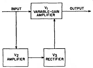
Fig. 65--Block diagram of volume compressor or expander circuit.
Tubes having a large dynamic range provide the best results in volume compressor or expander applications.
An example of this type is the 6BJ6.
Push-pull operation is generally desired for the variable-gain amplifier to prevent high distortion and other un desirable effects which may occur in volume compressors and expanders.
Phase Inverters
A phase inverter is a circuit used to provide resistance coupling between the output of a single-tube stage and the input of a push-pull stage. The necessity for a phase inverter arises because the signal-voltage inputs to the grids of a push-pull stage must be 180 degrees out of phase and approximately equal in amplitude with respect to each other. Thus, when the signal voltage input to a push-pull stage swings the grid of one tube in a positive direction, it should swing the grid of the other tube in a negative direction by a similar amount. With transformer coupling between stages, the out-of-phase input voltage to the push-pull stage is sup plied by means of the center-tapped secondary. With resistance coupling, the out-of-phase input voltage is obtained by means of the inverter action of a tube.
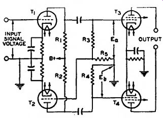
Fig. 66-Push-pull power amplifier resistance-coupled to triode by means
of phase inverter.
Fig. 66 shows a push-pull power amplifier, resistance-coupled by means of a phase-inverter circuit to a single stage triode T1. Phase inversion in this circuit is provided by triode T2. The output voltage of T1 is applied to the grid No. 1 of tetrode T3. A portion of the output voltage of Ti is also applied through the resistors Ra and R3 to the grid of T2 . The output voltage of T2 is applied to the grid No. 1 of tetrode TV
When the output voltage of T, swings in the positive direction, the plate current of T2 increases. This action increases the voltage drop across the plate resistor R2 and swings the plate of T2 in the negative direction. Thus, when the output voltage of T, swings positive, the output voltage of T2 swings negative and is, therefore, 180 degrees out of phase with the output voltage of T1.
In order to obtain equal voltages at E. and E„, (R, + R5)/R5 should equal the voltage gain of T2 . Under the condition where a twin-type tube or two tubes having the same characteristics are used as T1 and T2 , R< should be equal to the sum of R3 and Rs. The ratio of R3 + Rb to Rs should be the same as the voltage gain ratio of T2 in order to apply the correct value of signal voltage to T2. The value of R5 is, therefore, equal to R. divided by the voltage gain of T2; R3 is equal to R, minus R6. Values of R1, R2, R3 plus R6, and R< may be taken from the chart in the Resistance Coupled Amplifiers section. In the practical application of this circuit, it is convenient to use a twin-triode tube combining T1 and T2.
Tuned Amplifiers
In radio-frequency (rf) and inter mediate-frequency (if) amplifiers, the bandwidth of frequencies to be amplified is usually only a small percentage of the center frequency. Tuned amplifiers are used in these applications to select the desired bandwidth of frequencies and to suppress unwanted frequencies.
The selectivity of the amplifier is obtained by means of tuned interstage coupling networks.
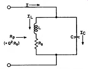
Fig. 67-Simple parallel resonant circuit.
The properties of tuned amplifiers depend upon the characteristics of resonant circuits. A simple parallel resonant circuit (sometimes called a "tank" because it stores energy) is shown in Fig. 67. For practical purposes the resonant frequency of such a circuit may be considered independent of the resistance R, provided R is small compared to the inductive reactance Xt.
The resonant frequency f, is then given by 2-vTjC
For any given resonant frequency, the product of L and C is a constant; at low frequencies LC is large; at high frequencies it is small.
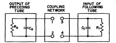
Fig. 68-Equivalent output and input circuits of tubes connected by a
coupling network.
The Q (selectivity) of a parallel resonant circuit alone is the ratio of the current in the tank (I r . or Ic) to the current in the line (I). This unloaded Q, or Qo, may be expressed in various ways, for example:
Ic Xr, R|, Q"- T ~ ~R - x7
where Xr, is the inductive reactance (= 2 pi fL), Xr is the capacitive reactance (= 1/[2-fCl), and R„ is the total impedance of the parallel resonant circuit
IC O 1
... (tank) at resonance. The Q varies inversely with the resistance of the inductor. The lower the resistance, the higher the Q and the greater the difference between the tank impedance at frequencies off resonance compared to the tank impedance at the resonant frequency.
The Q of a tuned interstage coupling network also depends upon the impedances of the preceding and following stages. The output impedance of a tube can be considered as consisting of a resistance R» in parallel with a capacitance Co, as shown in Fig. 68.
Similarly, the input impedance can be considered as consisting of a resistance R1 in parallel with a capacitance C1. Be cause the tuned circuit is shunted by both the output impedance of the pre ceding tube and the input impedance of the following tube, the effective selectivity of the circuit is the loaded Q (or Qr.) based upon the total impedance of the coupled network, as follows:
(total loading on) q _ l co'' at resonance) Xl or Xo
The capacitances Co and C1 in Fig. 68 are usually considered as part of the coupling network. For example, if the required capacitance between terminals 1 and 2 of the coupling network is calculated to be 500 picofarads and the value of C„ is 10 picofarads, a capacitor of 490 picofarads is used between terminals 1 and 2 so that the total capacitance is 500 picofarads. The same method is used to allow for the capacitance C1 at terminals 3 and 4.
When a tuned resonant circuit in the primary winding of a transformer is coupled to the nonresonant secondary winding of the transformer, as shown in Fig. 69, the effect of the input impedance of the following stage on the Q of the tuned circuit can be determined by considering the values reflected (or referred) to the primary circuit by transformer action. The reflected resistance ri is equal to the resistance R1 in the secondary circuit times the square of the effective turns ratio between the primary and secondary windings of the transformer T:
r, = Rt (N,/N2)' J where N1/N2
represents the electrical turns ratio between the primary winding and the secondary winding of T. If there is capacitance in the secondary circuit (C), it is reflected to the primary circuit as a capacitance C,>, and is given by:
C,„ = CP (N./NO*
The loaded Q, or Q1, is then calculated on the basis of the inductance LP, the total shunt resistance (Ro plus n plus the tuned-circuit impedance
Zt = Q»XC = QoX1), and the total capacitance (CP + CsP ) in the tuned circuit.
Fig. 70 shows a coupling network which consists of a single-tuned circuit using mutual inductive coupling. The capacitance Ct includes the effects of both the output capacitance of the pre ceding tube and the input capacitance of the following tube (referred to the primary of transformer Ti). The band width of a single-tuned transformer is determined by the half-power points on the resonance curve (-3 dB or 0.707 down from the maximum) . Under these conditions, the band pass Af is equal to the ratio of the center or resonant frequency fr divided by the loaded (effective) Q of the circuit, as follows:
Af = fr/QL

Fig. 68--Equivalent output and input circuits of tubes connected by a
coupling network.
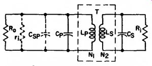
Fig. 69--Equivalent circuit for transformer coupling network having tuned
primary winding.

Fig. 70--Equivalent circuit for transformer coupling network using inductive
coupling.

Fig. 71--Single-tuned coupling network using capacitive division.
In high-frequency tuned amplifiers, where the input impedance is typically low, mutual inductive coupling may be impracticable because of the small number of turns in the secondary winding. It is extremely difficult in practice to construct a fractional part of a turn.
In such cases, capacitance coupling may be used, as shown in Fig. 71. This arrangement, which is also called capacitive division, is similar to tapping down on a coil at or near resonance.
Impedance transformation in this net work is determined by the ratio between capacitors G and C2. Capacitor C1 is normally much smaller than C2 ; thus the capacitive reactance Xci is normally much larger than Xcs. Provided the in put resistance of the following tube is much greater than Xcs, the effective turns ratio from the top of the coil to the input of the following tube is (0 + Cj)/ C1. The total capacitance Ct across the inductance L is given by C,C,
^ - C, + Ca
The resonant frequency fr is then given by 1 Double-tuned interstage coupling networks are often used in preference to single-tuned networks to provide flatter frequency response within the pass band, a sharper drop in response immediately adjacent to the ends of the pass band, or more attenuation at frequencies far removed from resonance.
In synchronous double-tuned networks, both the resonant circuit in the input of the coupling network and the resonant circuit in the output are tuned to the same resonant frequency. In "stagger-tuned" networks, the two resonant circuits are tuned to slightly different resonant frequencies to provide a more rectangular band pass with sharper selectivity at the ends of the pass band.
Double-tuned or stagger-tuned networks may use capacitive, inductive, or mutual inductance coupling, or any combination of the three.
Television Tuners
The vhf tuner of a television receiver selects the desired frequency channel in the range from 55 to 216 MHz, amplifies it, and converts it to a lower intermediate frequency. These functions are accomplished in rf-amplifier, mixer, and local-oscillator stages employing tube types that are designed specifically for these applications. The rf-amplifier stage uses a high-transconductance tube that has small dimensions to maintain low interelectrode capacitances, particularly between grid and plate. The mixer and oscillator stages usually employ a dual-unit triode-pentode unit and a medium-mu triode unit.
Fig. 72 shows a simplified schematic diagram of a typical vhf television tuner. The balun converts the 300 ohm balanced antenna impedance to an unbalanced impedance of 75 ohms. The high-pass filter eliminates lower-frequency interference signals. The tuner is set to the desired frequency by simultaneous adjustment of the inductances indicated by the several sets of arrows in Fig. 72. The inductances are either replaced completely or incremental amounts of inductance are added as the tuner is switched from high frequencies to lower frequencies. Some tuners use a combination of the two methods.
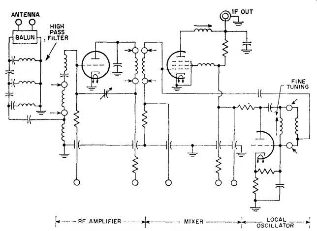
Fig. 72--Simplified schematic of typical vhf television tuner.
Because noise generated in the first amplifier stage is often the controlling factor in determining the over-all sensitivity of a radio or television receiver, the "front end" is designed with special attention to both gain and noise characteristics. The input circuit of an amplifier inherently contains some thermal noise contributed by the resistive elements in the input device. When an input signal is amplified, therefore, the thermal noise generated in the input circuit is also amplified. If the ratio of signal power to noise power (signal-to noise ratio, S/N) is the same in the output circuit as in the input circuit, the amplifier is considered to be "noise- less," and is said to have a noise figure of unity, or zero dB.
In practical circuits, however, all amplifier stages generate a certain amount of noise as a result of thermal agitation of electrons in resistors and other components, minute variations in the cathode emission of tubes (shot effect), and minute grid currents in the amplifier tubes. As a result, the ratio of signal power to noise power is inevitably impaired during amplification.
A measure of the degree of impairment is called the noise figure (NF) of the amplifier, and is expressed as the ratio of signal power to noise power at the input (Si/Ni) divided by the ratio of signal power to noise power at the output (So/N„), as follows:
(Si/NO of 10, and a 20-dB noise figure by a factor of 100.
The over-all noise figure of a receiver is affected by the total number of stages, as shown by the following relationship:
(NFa + 0 NF,.ceiver = NFl+ (NFs + 1)
+ GiG» NF: (So/No)
The noise figure in decibels (dB) is equal to ten times the logarithm of this power ratio. For example, a one-dB noise figure in an amplifier decreases the signal-to-noise ratio by a factor of 1.26, a 3-dB noise figure by a factor of 2, a 10-dB noise figure by a factor where G represents power gain and the subscripts indicate the number of each stage. This relationship indicates that the contribution of the second-stage noise factor to that of the over-all receiver is reduced by the gain of the first stage. Therefore, it is important that the rf amplifier have enough gain to make the effect of the second stage negligible. The third stage will then have even less effect. The maximum available power gain G of an rf stage is given by:
_ gm' Rin Rout G= -A
For maximum gain, therefore, the rf amplifier tube should have high trans conductance and high input and output impedances. At frequencies in the vhf television band, the input resistance is small enough to affect the gain. As mentioned previously, the rf tube is designed to have low interelectrode capacitances, small interelectrode spacings, and low lead inductances (particularly the cathode lead).
The gain of the rf stage must be reduced as the incoming-signal amplitude changes to prevent overload distortion in the following stages. As the signal amplitude increases, an automatic-gain-control (age) circuit biases the rf tube to decrease its gain. The rf tube usually employs a semi-remote cutoff grid to reduce cross-modulation distortion.
Either a triode or a pentode can be used in the rf-amplifier stage of tuner input circuits of vhf television receivers. Such stages are required to amplify signals ranging from 55 to 216 MHz and having a bandwidth of 4.5 MHz (the tuner is usually aligned for a bandwidth of 6 MHz to assure complete coverage of the band). In early rf tuners, pentodes rather than triodes were used because the grid-plate capacitance of triodes created stability problems.
However, the use of twin triodes in direct-coupled cathode-drive circuits makes it possible to obtain stable operation along with the low-noise characteristics of triodes.
Pentodes or tetrodes do not provide the useful sensitivity of triodes because of the "partition noise" introduced by the screen grid. The direct coupled cathode-drive circuit provides both the gain and the stability capabilities of the pentode, as well as the ad vantages of a low-noise triode input stage. Because the cathode-drive stage provides a low-impedance load to the grounded-cathode stage, the gain of the latter stage is very low and there is no necessity for neutralizing the grid-plate capacitance. An interstage impedance, usually an inductance in series with the plate of the first stage and the cathode of the second stage, is often used at higher frequencies to provide a degree of impedance matching between the units. The cathode-drive portion of the circuit is matched to the input net work and provides most of the stage gain. Because the feedback path of the cathode-drive circuit is the plate-cathode capacitance, which in most cases is very small, excellent isolation is provided between the antenna and the local oscillator.
Development of single triodes having low grid-plate capacitance, such as the 6BN4A has made possible the design of neutralized triode rf circuits.
Tubes such as the 6GK5 and 6CW4 are specially designed to minimize grid plate capacitance to permit easier neutralization of a grounded-cathode circuit over the wide frequency band.
Bridge-neutralized rf-amplifier stages are widely used in television tuners; in this arrangement, a portion of the output signal is returned to the grid out of phase with the feedback signal from the grid-plate capacitance. This circuit provides excellent gain and noise performance with stable operation across the band.
The mixer stage of a vhf tuner usually employs a pentode tube, or the pentode unit of a triode-pentode tube.
Although triodes such as the 6J6A were used as mixers in early receivers, they have been replaced by pentodes because the higher output impedance of a pentode provides a higher mixer gain than can be obtained with a triode.
The amplified signal from the rf stage in Fig. 72 is applied to the mixer grid along with a local-oscillator signal of much larger amplitude. The local oscillator signal varies the mixer grid voltage from cutoff into the grid-current region. This signal develops a grid resistor bias, called the injection voltage, which is a measure of the local-oscillator voltage. Because the transfer curve of the mixer tube is nonlinear, mixing action between the rf signal and the local-oscillator signal produces sum and difference frequencies. The output circuit of the mixer is tuned to the difference frequency (about 44 MHz) and rejects all other frequencies. This signal is then fed to the intermediate-frequency amplifier.
The mixer gain is a function of the amplitude of the local-oscillator signal. The gain has a broad maximum over a range of injection voltages from -2.5 to -5.0 volts for conventional grid mixers and slightly lower for frame-grid mixers. Good impedance matching between the rf-amplifier plate and the mixer grid, consistent with bandpass requirements, is important to achieve maximum signal power transfer. A slight amount of regeneration is provided by a small screen-grid inductance. This regeneration effectively increases the mixer-grid input impedance and thus improves power gain.
The local-oscillator stage shown in Fig. 72 is a Colpitts type in which the tuned circuit is located between the grid and plate and the feedback path is through the tube interelectrode capacitances. A large signal is developed in the local oscillator and coupled loosely to the mixer grid to minimize the effects of changes in the mixer in put on the frequency of oscillation.
The circuit is designed to keep frequency shift within a very narrow range with supply-voltage and temperature changes. Fine tuning is provided by a variable inductance or capacitance across the tuned circuit. Tubes commonly used in local-oscillator and mixer circuits are the 6EA8, 6KZ8, and 6KE8.
Television IF Amplifiers
The intermediate-frequency (if) amplifier stages in a television receiver provide the additional gain required to bring the signal level to an amplitude suitable for final detection. A constant peak signal of about three to five volts is required at the input to the detector.
The mixer output signal is passed through two or three stages of amplification to attain this level. High-trans conductance pentodes having low grid No. 1-to-plate capacitances are normally used in if amplifiers. The coupling circuits are usually tuned transformers which may be single- or double-tuned.
The transformers are either synchronously (same frequency) tuned or stagger-tuned, depending on circuit requirements. The over-all bandwidth varies from a maximum of 3.58 MHz at the 6-dB points for color receivers to values in the order of 2.0 to 2.5 MHz for the most inexpensive receivers. An expression for the figure of merit for a single tuned if-amplifier tube is the gain bandwidth product G X B, which is given by where C is the total tuning capacitance. This relationship again demonstrates the need for high transconductance and low interelectrode capacitance.
The first stage (or first two stages in the case of a three-stage if) is gain controlled like the rf amplifier. however, the bias applied to the if-amplifier tube varies the input resistance and capacitance of the tube and thus detunes the circuit. It is important for proper reception to maintain the frequency response of the if stages constant, particularly in the .case of the color receiver. Therefore, a small un bypassed cathode resistor is used which provides degenerative feedback to minimize the effect of bias changes. In addition, the effects on input impedance caused by the grid-plate capacitance are reduced by use of a partial bypass capacitor at the screen grid to provide neutralization of the grid-to-plate capacitance.
Tubes used in the gain-controlled stages of the if amplifier have remote or semi-remote-cutoff characteristics to reduce cross-modulation or intermodulation interference. Tube types commonly used in this application include the 6BZ6, 6GM6, 6JH6, 6ID6A, and 6KT6.
The last if-amplifier stage is a relatively-large-signal amplifier. For this reason, the tube must be biased so that it will operate over a region of linear operation for large voltage excursions. Because such a quiescent operating point provides a transconductance somewhat below the maximum value for the tube, the selection of the operating point involves a compromise between signal-handling capacity and gain. For purposes of linearity, the final if-amplifier stage is not gain-con trolled, and operates with the cathode bypassed to ground. Because fixed bias is used, a sharp-cutoff tube is used to provide higher transconductance than could be obtained with an equivalent remote- or semi-remote-cutoff tube. Examples of types used in this stage are the 6EW6 and 6JC6A.
Wideband (Video) Amplifiers
In some applications, it is necessary for a circuit to amplify signals ranging from very low frequencies (several hertz) to high frequencies (tens of megahertz) with a minimum of frequency and time-delay distortion. For example, very exacting requirements are demanded for such applications as television camera chains, ac voltmeters, and vertical amplifiers for oscilloscopes.
In response to these demands, circuit compensation techniques have been developed to minimize the amplitude and time-delay variation as the upper or lower frequency limits of the amplifier are approached.
The need for such compensation is evident when many identical stages of amplification are employed. If ten cascaded stages are used, a variation of 0.3 dB per stage results in a total variation of 3 dB. In an uncompensated amplifier, this total variation occurs two octaves (a frequency ratio of four) prior to the half-power point. Because two octaves are lost from both the high and low frequencies, the band width of ten cascaded uncompensated amplifies stages is only one-sixteenth that of a single amplifier stage. Fig. 73 shows the amplitude response characteristics of various numbers of identical uncompensated amplifiers.
In general, the output of an amplifier may be represented by a current generator i_out and a load resistance R1, as shown in Fig. 74(a). Because the signal current is shunted by various capacitances at high frequencies, as shown in Fig. 74(b), there is a loss in gain at these frequencies. If an inductor L is placed in series with the load resistor RL, as shown in Fig. 74(c), a low-Q circuit is formed which some what suppresses the capacitive loading.
This method of gain compensation, called shunt peaking, can be effective for improving high-frequency response.
Fig. 74 shows the frequency response for the circuits in Fig. 74(a), (b), and (c).
If the inductor L in Fig. 74(c) is made self-resonant approximately one octave above the 3-dB frequency of the circuit of Fig. 74(b), the amplifier response is extended by about another 30 percent.
If the stray capacitance C shown in Fig. 74(b) is broken into two parts C and C" and an inductor Li is placed between them, a heavily damped form of series resonance may be employed for further improvement. This form of compensation, called series peaking, is shown in Fig. 75(a). If C and C" are within a factor of two of each other, series peaking produces an appreciable improvement in frequency response as compared to shunt peaking. A more complex form of compensation embodying both self-resonant shunt peaking and series peaking is shown in Fig. 75(b).
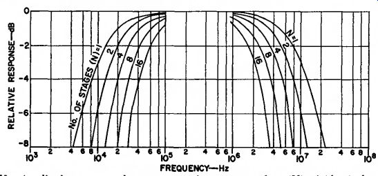
Fig. 73--Amplitude response characteristics of various numbers (N) of
identical uncompensated amplifiers.
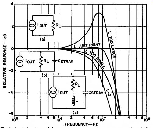
Fig. 74--Equivalent circuits and frequency response of uncompensated
and shunt-peaked amplifiers.
The effects of various high-frequency compensation systems can be demonstrated by consideration of an amplifier consisting of three identical stages. If each of the three stages is down 3 dB at 1 MHz, and if a total gain variation of plus 1 dB and minus 3 dB is allowed, the bandwidth of the amplifier is 0.5 MHz without compensation. Shunt peaking raises the bandwidth to 1.3 MHz. Self-resonant shunt peaking raises it to 1.5 MHz. An in finitely complicated network of shunt peaking techniques could raise it to 2 MHz. If the distribution of capacitance permits it, series peaking alone can provide a bandwidth of about 2 MHz, while a combination of shunt and series peaking can provide a bandwidth of approximately 2.8 MHz. If the capacitance is perfectly distributed, and if an infinitely complex network of shunt and series peaking is employed, the ultimate capability is about 4 MHz.
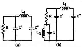
Fig. 75-- Circuits using (a) series peaking, and (b) both self-resonant
shunt peaking and series peaking.
The frequency response of a wide band amplifier is influenced greatly by variations in component values due to temperature effects, variation of tube parameters with voltage and current (normal large-signal excursions), changes of stray capacitance due to relocated lead wires, or other variations.
A change of 20 percent in any of the critical parameters can cause a change of 0.7 dB in gain per stage over the last half-octave of the response for the most simple case of shunt peaking.
As the bandwidth is extended by more complex peaking, a circuit becomes substantially more critical. Measurement probes generally alter circuit performance because of their capacitance; this effect should be considered during frequency-response measurements.
In the design of wideband amplifiers using many stages of amplification, it is necessary to consider time delay variations as well as amplitude variation. When feedback capacitance is a major contributor to response limitation, the more complex compensating networks may produce severe ringing or even sustained oscillation. If feedback capacitance is treated as input capacitance produced by the Miller effect, the added input capacitance Ct ' caused by the feedback capacitor Cf is given by C = C, (1 - VG) where VG is the input-to-output voltage gain. The gain VG, however, has a phase angle that varies with frequency. The phase angle is 180 degrees at low frequencies, but may lead or lag this value at high frequencies; the magnitude of VG then also varies. In the design of very wideband amplifiers (20 MHz or more), the phase of the transconductance g,„ must be considered.
The video amplifier stage in a television receiver usually employs a pentode-type tube specially designed to amplify the wide band of frequencies contained in the video signal and, at the same time, to provide high gain per stage. Pentodes are more useful than triodes in such stages because they have high transconductance (to provide high gain) together with low input and output interelectrode capacitances (to permit the broadband requirements to be satisfied). An approximate "figure of merit" for a particular tube for this application can be determined from the ratio of its transconductance, go,, to the sum of its input and output capacitances, Cm and com, as follows:
Figure of Merit :
C in 4- Com
Typical values for this figure are in the order of 500 x 10' or greater.
A typical video amplifier stage, such as that shown in Fig. 76, is connected between the second detector of the television receiver and the picture tube. The contrast control, R1, in this circuit controls the gain of the video amplifier tube. The inductance, 1-2, m series with the load resistor, RL, maintains the plate load impedance at a relatively constant value with increasing frequency. The inductance L1 isolates the output capacitance of the tube so that only stray capacitance is placed
across the load. As a result, a higher value load resistor is used to provide higher gain without affecting frequency response or phase relations. The decoupling circuit, C1R2, is used to improve the low-frequency response.
Tubes used as video amplifiers include types 6CL6 and 12BY7A, or the pentode sections of types 6AW8A and 6AN8A.
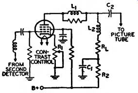
Fig. 76-Typical video amplifier stage.
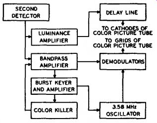
Fig. 77-Block diagram of video-amplifier section of color television
receiver.
The luminance amplifier in a color television receiver is a conventional video amplifier having a bandwidth of approximately 3.5 MHz. In a color receiver, the portion of the output of the second detector which lies within the frequency band from approximately 2.4 to 4.5 MHz is fed to a bandpass amplifier, as shown in the block diagram in Fig. 77. The color synchronizing signal, or "burst," contained in this signal may then be fed to a "burst-keyer" tube. At the same time, a delayed horizontal pulse may be applied to the keyer tube. The output of the keyer tube is applied to the burst amplifier tube and the signal is then fed to the 3.58-MHz oscillator and to the "color-killer" stage.
The color killer applies a bias voltage to the bandpass amplifier in the absence of burst so that the color section, or chrominance channel, of the receiver remains inoperative during black-and white broadcasts. A threshold control varies the bias and controls the burst level at which the killer stage operates.
The output of the 3.58-MHz oscillator and the output of the bandpass amplifier are fed into phase and amplitude demodulator circuits. The output of each demodulator circuit is an electrical representation of a color-difference signal, i.e., an actual color signal minus the black-and-white, or luminance, signal. The two color-difference signals are combined to produce the third color-difference signal; each of the three signals then represents one of the primary colors.
The three color-difference signals are usually applied to the grids of the three electron guns of the color picture tube, in which case the black-and-white signal from the luminance amplifier may be applied simultaneously to the cathodes. The chrominance and luminance signals then combine to produce the color picture. In the absence of transmitted color information, the chrominance channel is cut off by the color killer, as described above, and only the luminance signal is applied to the picture tube, producing a black-and-white picture.
TV Scanning, Sync, and Deflection
For reproduction of a transmitted picture in a television receiver, the face of a cathode-ray tube is scanned with an electron beam while the intensity of the beam is varied to control the emitted light at the phosphor screen. The scanning is synchronized with a scanned image at the TV transmitter, and the black-through-white picture areas of the scanned image are converted into an electrical signal that controls the intensity of the electron beam in the picture tube at the receiver.

Fig. 78-The odd-line interlaced scanning procedure.
Scanning Fundamentals
The scanning procedure used in the United States employs horizontal linear scanning in an odd-line inter laced pattern. The standard scanning pattern for television systems includes a total of 525 horizontal scanning lines in a rectangular frame having an aspect ratio of 4 to 3. The frames are repeated at a rate of 30 per second, with two fields interlaced in each frame. The first field in each frame consists of all odd-number scanning lines, and the second field in each frame consists of all even-number scanning lines. The field repetition rate is thus 60 per second, and the vertical scanning rate is 60 Hz.
The geometry of the standard odd line interlaced scanning pattern is illustrated in Fig. 78. The scanning beam starts at the upper left corner of the frame at point A, and sweeps across the frame with uniform velocity to cover all the picture elements in one horizontal line. At the end of each trace, the beam is rapidly returned to the left side of the frame, as shown by the dashed line, to begin the next horizontal line. The horizontal lines slope downward in the direction of scanning because the vertical deflecting signal simultaneously produces a vertical scanning motion, which is very slow compared with the horizontal scanning speed. The slope of the horizontal line trace from left to right is greater than the slope of the retrace from right to left because the shorter time of the retrace does not allow as much time for vertical deflection of the beam. Thus, the beam is continuously and slowly deflected downward as it scans the horizontal lines, and its position is successively lower as the horizontal scanning proceeds.
At the bottom of the field, the vertical retrace begins, and the beam is brought back to the top of the frame to begin the second or even-number field. The vertical "flyback" time is very fast compared to the trace, but is slow compared to the horizontal scanning speed; therefore, some horizontal lines are produced during the vertical flyback.
All odd-number fields begin at point A in Fig. 78 and are the same.
All even-number fields begin at point C and are the same. Because the be ginning of the even-field scanning at C is on the same horizontal level as A, with a separation of one-half line, and the slope of all lines is the same, the even-number lines in the even fields fall exactly between the odd-number lines in the odd field.
Sync
In addition to picture information, the composite video signal from the video detector of a television receiver contains timing pulses to assure that the picture is produced on the face plate of the picture tube at the right instant and in the right location. These pulses, which are called sync pulses, control the horizontal and vertical scanning generators of the receiver.
Fig. 79 shows a portion of the detected video signal. When the picture is bright, the amplitude of the signal is low. Successively deeper grays are represented by higher amplitudes until, at the "blanking level" shown in the diagram, the amplitude represents a complete absence of light. This "black level" is held constant at a value equal to 75 percent of the maximum amplitude of the signal during transmission.
The remaining 25 percent of the signal amplitude is used for synchronization information. Portions of the signal in this region (above the black level) can not produce light.
In the transmission of a television picture, the camera becomes inactive at the conclusion of each horizontal line and no picture information is transmitted while the scanning beam is retracing to the beginning of the next line. The scanning beam of the receiver is maintained at the black level during this retrace interval by means of the blanking pulse shown in Fig. 79.
Immediately after the beginning of the blanking period, the signal amplitude rises further above the black level to provide a horizontal-synchronization pulse that initiates the action of the horizontal scanning generator. When the bottom line of the picture is reached, a similar vertical-synchronization pulse initiates the action of the vertical scanning generator to move the scanning spot back to the top of the pattern.
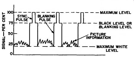
Fig. 79--Detected video signal.
The sync pulses in the composite video signal may be separated from the video information in the output of the second or video detector by means of the triode circuit shown in Fig. 80. In this circuit, the time constant of the network R1C1 is long with respect to the interval between pulses. During each pulse, the grid is driven positive and draws current, thereby charging capacitor G.
Consequently, the grid develops a bias which is slightly greater than the cutoff voltage of the tube.
Because plate current flows only during the sync-pulse period, only the amplified pulse appears in the output.
This sync-separator stage discriminates against the video information. Because the bias developed on the grid is proportional to the strength of the in coming signal, the circuit also has the advantage of being relatively independent of signal fluctuations.
After the synchronizing signals are separated from the composite video signal, it is necessary to filter out the horizontal and vertical sync signals so that each can be applied to its respective deflection generator. This filtering is accomplished by RC circuits designed to filter out all but the desired synchronizing signals. Although the horizontal, vertical, and equalizing pulses are all rectangular pulses of the same amplitude, they differ in frequency and pulse width, as shown in Fig. 81. The horizontal sync pulses have a repetition rate of 15,750 per second (one for each horizontal line) and a pulse width of 5.1 microseconds. The equalizing pulses have a width approximately half the horizontal pulse width, and a repetition rate of 31,500 per second; they occur at half-line intervals, with six pulses immediately preceding and six following the vertical synchronizing pulse. The vertical pulse is repeated at a rate of 60 per second (one for each field), and has a width of approximately 190 microseconds. The serrations in the vertical pulse occur at half-line intervals, dividing the complete pulse into six individual pulses that provide horizontal synchronization during the vertical retrace. (Although the picture is blanked out during the vertical retrace time, it is necessary to keep the horizontal scanning generator synchronized.)
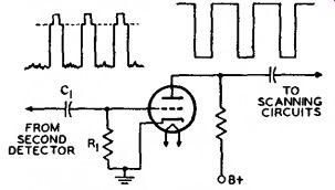
Fig. 80-Sync-separator circuit.

Fig. 81-Waveform of TV synchronizing pulses (H - horizontal line period
of 1/15,750 seconds, or 63.5 u-s).
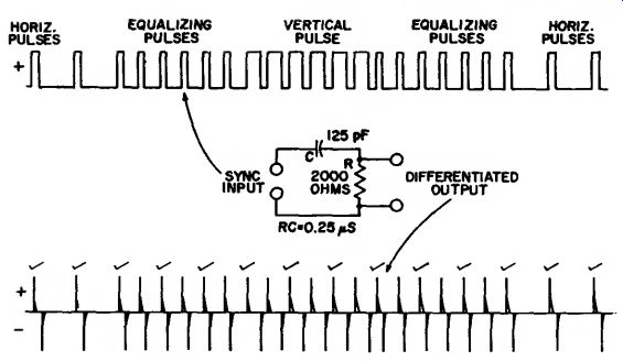
Fig. 82-Separation of the horizontal sync signals from the total sync
by a differentiating circuit.
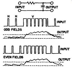
Fig. 83-Separation of vertical sync signals from the total sync for
odd and even fields with no equalizing pulses. (Dashed line indicates
triggering level for vertical scanning generator.)
All the pulses described above are produced at the transmitter by the synchronizing-pulse generator; their waveshapes and spacings are held within very close tolerances to provide the required synchronization of receiver and transmitter scanning.
The horizontal sync signals are separated from the total sync in a differentiating circuit that has a short time constant compared to the width of the horizontal pulses. When the total sync signal is applied to the differentiating circuit shown in Fig. 82, the capacitor charges completely very soon after the leading edge of each pulse, and remains charged for a period of time equal to practically the entire pulse width. When the applied voltage is removed at the time corresponding to the trailing edge of each pulse, the capacitor discharges completely within a very short time. As a result, a positive peak of voltage is obtained for each leading edge and a negative peak for the trailing edge of every pulse.
One polarity is produced by the charging current for the leading edge of the applied pulse, and the opposite polarity is obtained from the discharge current corresponding to the trailing edge of the pulse.
As mentioned above, the serrations in the vertical pulse are inserted to provide the differentiated output needed to synchronize the horizontal scanning generator during the time of vertical synchronization. During the vertical blanking period, many more voltage peaks are available than are necessary for horizontal synchronization (only one pulse is used for each horizontal line period). The check marks above the differentiated output in Fig. 82 indicate the voltage peaks used to synchronize the horizontal deflection generator for one field. Because the sync system is made sensitive only to positive pulses occurring at approximately the right horizontal timing, the negative sync pulses and alternate differentiated positive pulses produced by the equalizing pulses and the serrated vertical information have no effect on horizontal timing. It can be seen that although the total sync signal (including vertical synchronizing information) is applied to the circuit of Fig. 82, only horizontal synchronization information appears at the output.
The vertical sync signal is separated from the total sync in an integrating circuit which has a time constant that is long compared with the duration of the 5-microsecond horizontal pulses, but short compared with the 190-micro second vertical pulse width. Fig. 83 shows the general circuit configuration used, together with the input and output signals for both odd and even fields.
The period between horizontal pulses, when no voltage is applied to the RC circuit, is so much longer than the horizontal pulse width that the ' capacitor has time to discharge almost down to zero. When the vertical pulse is applied, however, the integrated voltage across the capacitor builds up to the value required for triggering the vertical scanning generator. This integrated voltage across the capacitor reaches its maximum amplitude at the end of the vertical pulse, and then declines practically to zero, producing a pulse of the triangular wave shape shown for the complete vertical synchronizing pulse. Although the total sync signal (including horizontal information) is applied to the circuit of Fig. 83, there fore, only vertical synchronization in formation appears at the output.
The vertical synchronizing pulses are repeated in the total sync signal at the field frequency of 60 per second. Therefore, the integrated output voltage across the capacitor of the RC circuit of Fig. 83 can be coupled to the vertical scanning generator to provide vertical synchronization. The six equalizing pulses immediately preceding and following the vertical pulse improve the accuracy of the vertical synchronization for better interlacing.
The equalizing pulses that precede the vertical pulses make the average value of applied voltage more nearly the same for even and odd fields, so that the integrated voltage across the capacitor adjusts to practically equal values for the two fields before the vertical pulse begins. The equalizing pulses that follow the vertical pulse minimize any difference in the trailing edge of the vertical synchronizing signal for even and odd fields.
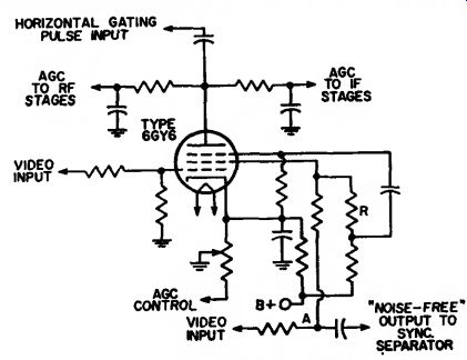
Fig. 84--Typical noise-cancellation circuit.
In fringe areas, two conditions complicate the process of sync separation. First, the incoming signal available at the antenna is weak and susceptible to fading and other variations; second, the receiver is operating at or near maximum gain, which makes it extremely susceptible to interference from pulse-type noise generated by certain types of electrical equipment, ignition systems, switches, or the like. Some type of noise-immunity provision is almost essential for acceptable performance. Noise may be reduced or eliminated from the sync and age circuits by gating or by a combination of gating, inversion, and cancellation. An example, of the latter method is shown in Fig. 84. In this circuit the 6GY6, which has two independent control grids, serves the dual function of age amplifier and noise inverter. Because the sync tips of the video signal at grid No. 1 of the 6GY6 drive the tube near its cutoff region, any noise signal extending above the tip level will appear inverted across the grid-No.2 load resistor R. This inverted noise signal is re-combined with the video signal and fed to the sync separator at point "A" in Fig. 84, where noise cancellation takes place. This process leaves the sync pulses relatively free of disturbing noise and results in a stable picture.
To prevent reduction of receiver gain due to the effect of noise on the age amplifier, a portion of the inverted noise signal is fed to the second control grid, grid No.3, of the 6GY6 to cut off or gate the age amplifier when a noise pulse occurs.
Horizontal Deflection
In the horizontal-deflection stages of a television receiver, a current that varies linearly with time and has a sufficient peak-to-peak amplitude must be passed through the horizontal-deflection-yoke winding to develop a magnetic field adequate to deflect the electron beam of the television picture tube. (This type of deflection is different from that used in a cathode-ray oscilloscope, where the beam is deflected electrostatically.) After the beam is deflected completely across the face of the picture tube, it must be returned very quickly to its starting point. (As explained previously, the beam is extinguished during this retrace by the blanking pulse incorporated in the composite video signal, or in some cases by additional external blanking derived from the horizontal deflection system.)
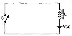
Fig. 85--Simplest form of deflection circuit.
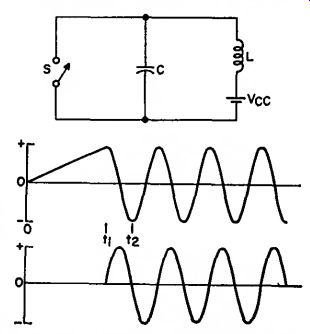
Fig. 86--Addition of capacitor to permit flyback ringing, and yoke-current
(upper) and switch-voltage (lower) waveforms.
The simplest form of a deflection circuit is shown in Fig. 85. In this circuit, the yoke impedance L is assumed to be a perfect inductor. When the switch is closed, the yoke current starts from zero and increases linearly. At any time t, the current i is equal to Et/L, where E is the applied voltage.
When the switch is opened at a later time ti, the current instantly drops from a value of Eti/L to zero.
Although the basic circuit of Fig. 85 crudely approaches the requirements for deflection, it presents some obvious problems and limitations. The voltage across the switch becomes extremely high, theoretically approaching infinity.
In addition, if very little of the total time is spent at zero current, the circuit would require a tremendous amount of dc power. Furthermore, the operation of the switch would be rather critical with regard to both its opening and its closing. Finally, because the deflection field would be phased in only one direction, the beam would have to be centered at the extreme left of the screen for zero yoke current.
If a capacitor is placed across the switch, as shown in Fig. 86, the yoke current still increases linearly when the switch is closed at time t - 0. however, when the switch is opened at time t = ti, a tuned circuit is formed by the parallel combination of L and C.
The resulting yoke currents and switch voltages are then as shown in Fig. 86.
The current is at a maximum when the voltage equals zero, and the voltage is at a maximum when the current equals zero. If it is assumed that there are no losses, the ringing frequency fo.c is equal to 1/(2jt\/LC).
If the switch is closed again at any time the capacitor voltage is not equal to zero, an infinite switch current flows as a result of the capacitive discharge.
However, if the switch is closed at the precise moment t2 that the capacitor voltage equals zero, the capacitor cur- rent effortlessly transfers to the switch, and a new transient condition results.
Fig. 87 shows the yoke-current and switch-voltage waveforms for this new condition.
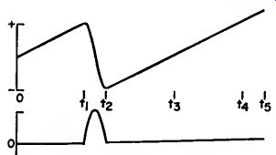
Fig. 87--Yoke-current (upper) and switch voltage (lower) waveforms when
switch is closed at t2.
If the switch is again opened at ti, closed at U, and so on, the desired sweep results, the peak switch voltage is finite, and the average supply current is zero. The deflection system is then lossless and efficient and, because the average yoke current is zero, beam de-centering is avoided. The only fault of the circuit of Fig. 86 is the critical timing of the switch, particularly at time t = U.
However, if the switch is shunted by a damper diode, as shown in Fig. 88, the diode acts as a closed switch as soon as the capacitor voltage reverses slightly. The switch may then be closed at any time between t2 and U.
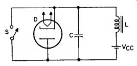
Fig. 88--Incorporation of damper diode.
Fig. 89 shows a typical horizontal output-and-deflection circuit used in television receivers. In addition to supplying the deflection energy required for horizontal deflection of the picture-tube beam, this circuit provides the high dc voltage required for the ultor (anode) of the picture tube and the "boosted" B voltage for other portions of the receiver.
The horizontal-output tube is usually a beam power tube such as the 6JB6A, 6JG6A, or 6LQ6/6JE6C.
In this circuit, a sawtooth voltage from the horizontal-oscillator tube is applied to the grid No. 1 of the horizontal-output tube. When this voltage rises above the cutoff point of the output tube, the tube conducts a sawtooth of plate current which is fed through the auto-transformer to the horizontal-deflecting yoke. At the end of the horizontal-scanning cycle, which lasts for 63.4 microseconds, the sawtooth voltage on the grid suddenly cuts off the output tube. This sudden change sets up an oscillation of about 50 to 70 kHz in the output circuit, which may be considered as an inductor shunted by the stray capacitance of the circuit. During the first half of this oscillation, a positive voltage appears across the transformer. In the second half of the cycle, the voltage swings below the plate supply voltage, and the damper diode conducts, damping out the oscillation. At the same time, the current through the deflecting yoke reverses and reaches its negative peak.
As the damper-diode current decays to zero, the output tube begins to conduct again. The yoke current, therefore, is composed of current resulting from damper-diode conduction followed by output-tube conduction.
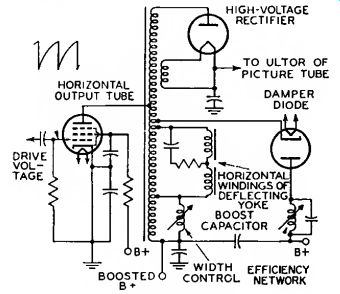
Fig. 89--Typical horizontal-deflection and high-voltage circuit.
When the output tube is suddenly cut off, the high-voltage pulse produced is increased by means of an extra winding on the transformer. This high voltage pulse charges a high-voltage capacitor through the high-voltage rectifier. The output of this circuit is the dc high-voltage supply for the picture tube. The high-voltage rectifier also obtains its filament power through a separate winding on the horizontal-output transformer.
Current flowing through the damper diode charges the "boost" capacitor through the damper portion of the trans former winding. The polarity of the charge on the capacitor is such that the voltage at the low end of the winding is increased above the plate supply voltage, or B-f. This higher voltage or "boost" is used for the output-tube plate supply, and may also supply the deflection oscillators and other low current-drain circuits in the receiver.
Vertical Deflection
The vertical-deflection circuit in a television receiver is essentially a class A audio amplifier with a complex load line, severe low-frequency requirements (much lower than 60 Hz), and a need for controlled linearity. The equivalent low-frequency response for a 10-percent deviation from linearity is 1 Hz.
The required performance can be obtained in a vertical-deflection circuit in any of three ways. The amplifier may be designed to provide a flat response down to 1 Hz. This design, however, requires an extremely large output transformer and immense capacitors. Another arrangement is to design the amplifier for fairly good low-frequency response and pre-distort the generated signal.
The third method is to provide extra gain so that feedback techniques can be used to provide linearity. If loop feedback of 20 or 30 dB is used, tube gain variations and nonlinearities become fairly insignificant. The feedback automatically provides the necessary "pre-distortion" to correct low frequency limitations. In addition, the coupling of miscellaneous signals (such as power-supply hum or horizontal deflection signals) in the amplifying loop is suppressed.
A modified multivibrator in which the vertical-output tube is part of the oscillator circuit is used in the vertical deflection stage of many television receivers. This stage supplies the deflection energy required for vertical deflection of the picture-tube beam. A simplified combined vertical-oscillator output stage is shown in Fig. 90. Wave shapes at critical points of the circuit are included to illustrate the development of the desired current through the vertical-output transformer and deflecting yoke.
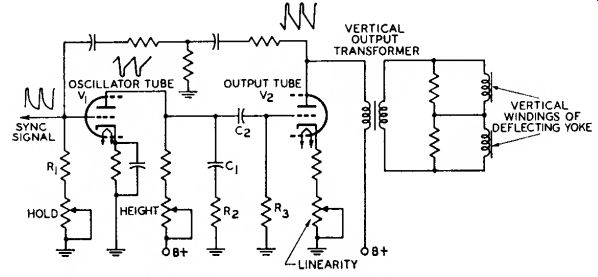
Fig. 90--Simplified combined vertical-oscillator-and-output stage.
The current waveform through the deflecting yoke and output transformer should be a sawtooth to provide the desired deflection. The grid and plate voltage waveforms of the output tube could also be sawtooth except for the effect of the inductive components in the yoke and transformer. The effect of these inductive components must be taken into consideration, however, particularly during retrace. The fast rate of current change during retrace time (which is approximately 1/15 as long as trace time) causes a high-voltage pulse a the plate which could give a trapezoidal waveshape to the plate voltage and cause increased plate current, excess damping, and lengthened retrace time.
However, the grid voltage is made sufficiently negative during retrace to keep the tube close to cutoff, as described below.
The frequency, and the relative deviation of the positive and negative portions of each cycle, are dependent on the values of resistors Rt and R3 and the RC combination R3C2, as explained in the section on multivibrators. The desired trapezoidal waveshape at the grid of V2 is created by capacitor C1 and resistor R2. If R2 were equal to zero, would cause the grid-voltage waveshape to take the form shown in Fig. 91(a). When R2 is sufficiently large, C1 does not discharge completely when Vi conducts. When V1 is cut off, there fore, the voltage on the grid of V2 immediately rises to the voltage across C1. The resulting waveshape is shown in Fig. 91(b). The negative-going pulse of the grid-voltage waveshape prevents the high plate pulse from causing excess conduction, and thereby prevents overdamping.
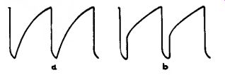
Fig. 91--Waveforms showing effect of R2 in Fig. 90.
This vertical-deflection stage utilizes twin-triode tubes such as the 6DR7 and 6GF7A. The 6GF7A is particularly suitable for this application because it incorporates dissimilar units to provide for the different operating requirements of the oscillator and output sections.
High-Voltage Regulation
In color television receivers, it is very important to regulate the high voltage supply for the picture tube.
Poor regulation of the high voltage can adversely affect the performance of the focusing and convergence circuits so that picture blooming results. In addition, excessive voltage or current may be applied to the high-voltage rectifier, horizontal-output tube, and horizontal output (flyback) transformer so that the useful life of these components is substantially shortened. In modern color television receivers, regulation of the high voltage is accomplished by use of a shunt-type electronic voltage regulator connected across the output of the high voltage power supply or by use of a pulse-type regulator connected in shunt with the flyback transformer.
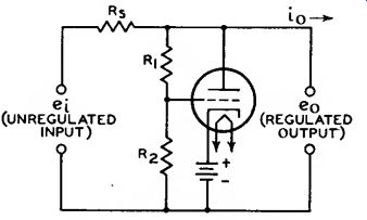
Fig. 92--High-voltage regulator circuit for color television.
Shunt Regulator Circuit
Fig. 92 shows the schematic diagram of a typical shunt regulator circuit. This circuit uses a 6BK4C/6EL4 or 6EN4 sharp cutoff beam triode for the regulator tube and is suitable for regulation of the output of a high-voltage, high impedance supply. The cathode of the regulator beam triode is held at a fixed positive potential with respect to ground. Because the grid potential is kept slightly less positive by the voltage drop across resistor R2, the tube operates in the negative grid region and no grid current is drawn.
When the output voltage, e„, rises as a result of a decrease in load current, a small fraction of the additional voltage is applied to the grid of the tube by the voltage-divider circuit consisting of Ri and R2. This increased grid voltage causes the tube to draw an increased current from the unregulated supply.
The increased current, in turn, causes a voltage drop across the high internal impedance of the unregulated supply, R„ which tends to counteract the original rise of the voltage. If desired, the grid may be connected to a variable point on the voltage divider to allow some adjustment of the output-voltage level.
The grid voltage for the regulator can also be obtained from a tap on the B-boost voltage supply. The use of this lower voltage (about 375 volts) eliminates the need for costly and trouble some high-voltage resistors. In this arrangement, variations in high voltage also vary the tapped-down B-boost voltage at the regulator grid, and the resulting variations in conduction of the regulator increase or decrease the loading of the high-voltage supply so that the total load remains nearly constant.
The shunt regulator circuit, in effect, presents a variable load impedance to the output of the high-voltage rectifier. Because the regulator is connected directly across the output of the rectifier, the regulator tube is required to handle the full amount of the high voltage (approximately 25 kilovolts) applied to the picture tube. The tube area, therefore, must be well shielded to provide adequate X-ray protection, and a relatively large area is required for voltage insulation. In addition, the high-voltage rectifier is required to conduct full-load current continuously. The shunt regulator maintains a constant high voltage by sensing changes in the B Boost voltage, which are indicative of changes in beam current, and increasing or decreasing conduction accordingly.
Pulse Regulator Circuit--In a pulse-regulator system, the regulator circuit is effectively shunted across part of the horizontal winding of the horizontal-output transformer. During operation, the pulse-regulator circuit maintains a substantially constant pulse amplitude in the primary winding of the horizontal-output transformer with changing loads on the high-voltage power supply. A constant-amplitude, stepped-up pulse is then applied to the high-voltage rectifier tube, arid the high voltage developed from this pulse is maintained at a constant value. In the pulse-regulator system, regulator control is achieved by sampling the picture tube current by means of a special winding on the fly-back transformer and use of the resultant voltage drop (across a resistor) to control the grid circuit of the regulator tube.
Fig. 93 shows the schematic diagram and significant waveforms for a circuit that uses a 17KV6A beam-power pentode for the regulator tube. During trace and retrace, the cathode of the 17KV6A is held at B+. During the trace period, the screen grid of the 17KV6A is biased well below the cathode voltage and is unaffected by the beam current drawn by the picture tube. The control-grid bias is determined by the resistive voltage-divider network Rs, R3 , R4, and is directly dependent on the beam current of the picture tube. The damper tube conducts during the trace period and holds the plate potential of the 17KV6A at B+. With the plate-to-cathode potential at zero and the screen grid negative with respect to the cathode, the regulator tube is completely cut off during the trace period. At the start of the retrace period, however, the damper tube be comes reverse-biased, and the voltage on the plate of the regulator tube begins to rise. This increasing voltage is coupled to the screen grid through C1 and R1 and to the control grid through the interelectrode capacitance of the tube.
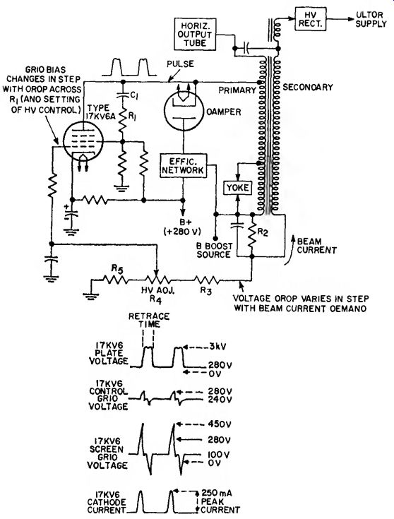
Fig. 93--Schematic diagram and significant waveforms for a typical pulse-regulator
circuit.
The waveforms in Fig. 93 show that at the start of retrace the plate and screen grid of the 17KV6A have both been driven positive with respect to the cathode and the control grid has become less negative with respect to the cathode. The regulator tube then begins to conduct. The pulses impressed on the screen and control grids are short in duration so that the screen grid remains positive with respect to the cathode and the control grid remains near cathode potential for only a short time. The regulator tube is driven into conduction for approximately 2 to 4 microseconds at the start of retrace and is then cut off. As the beam current ' increases or decreases, the voltage developed across the resistive voltage-divider network R2, R3, R4, and R5 tracks these changes and is applied to the control grid of the regulator tube. In this way, the conduction of the regulator tube is increased or decreased as required to maintain a constant high-voltage output. By removal of the energy from the rising edge of the flyback pulse in this fashion, the height of the pulse used to develop the high voltage is controlled.
At the same time interference with the shape of the deflection pulse is held to a minimum.
Color Demodulation
In the transmission of picture signals for color-television receivers, all the color information is contained in three signals, a luminance (black-and white) or monochrome signal and two chrominance signals. The luminance signal, which is called the Y signal, contains brightness information only. The voltage response of the Y signal is made similar to the brightness response of the human eye by use of a composite signal that contains definite proportions of the red, green, and blue signals from the color-television camera (30 percent red, 59 percent green, and 11 percent blue). This Y signal, which includes sync and blanking pulses, provides a correct monochrome picture in a conventional black-and-white television receiver.
For the generation of color-television signals, the Y signal is subtracted from the red, green, and blue signals to provide a new set of color-difference signals, which are designated as R-Y, B-Y, and G-Y. All of the original picture information is contained in the Y signal, the R-Y signal, and the B-Y signal. Therefore, the G-Y signal is not contained in the transmitted signal, but is synthesized in the receiver by proper combination of the R-Y and B-Y signals.
(Color signals transmitted under present color-television standards are not R-Y and B-Y, but a similar pair of signals designated as I and Q. In the color-television receiver, R-Y and B-Y signals are demodulated directly from the I and Q signals with negligible loss of color quality. For purposes of simplicity, only R-Y and B-Y signals are considered in this explanation. In addition, a 90-degree phase-shift network is shown; the phase-shift angle could be, and often is, some other value.)
Because the luminance signal and the two color-difference signals must be transmitted with a standard 6-MHz channel, the two color signals are combined into one signal at the transmitter and are independently recovered at the receiver by proper detection techniques. A color subcarrier of approximately 3.58 MHz is used for transmitting the color information within the 6-MHz spectrum of the television station. As shown in Fig. 94, the 3.58-MHz subcarrier and one of the color-difference signals are applied directly to a balanced AM modulator.
The other color-difference signal is applied directly to a second balanced AM modulator, and the 3.58-MHz subcarrier is applied to this second modulator through a 90-degree phase-shifting net work. The balanced modulators effectively cancel both the individual color difference signals and the subcarrier signal, and the output contains only the sidebands of the combined chrominance signal.

Fig. 94-Formation of combined color signal for transmission.
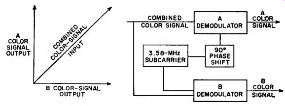
Fig. 95-Separation of combined color signal into two signals at the
receiver.
Recovery of the color information at the receiver involves a process called synchronous detection. In this process, two separate detectors are used to recover the separate color information, just as two separate modulators were used to combine the information at the transmitter. The 3.58-MHz subcarrier, which was suppressed during transmission, must be reinserted at the receiver for recovery of the color information.
The basis of synchronous detection is the phase relationship of this reinserted 3.58-MHz sub-carrier.
For example, the original color in formation is represented in Fig. 94 by the color-difference signals A and B.
At the receiver, the combined color signal is fed to two demodulators A and B, as shown in Fig. 95. At the same time, a 3.58-MHz subcarrier is also fed to the two demodulators, with the same phase relationship that was used in the modulators at the transmitter. This locally generated subcarrier essentially duplicates or replaces the original subcarrier, which was removed at the transmitter.
The local 3.58-MHz oscillator in the color-television receiver is made to function at the proper frequency and phase by means of a synchronizing signal sent out by the transmitter. This synchronizing signal consists of a short burst of 3.58-MHz signals transmitted during the horizontal blanking interval, immediately after the horizontal sync pulse, as shown in Fig. 96.
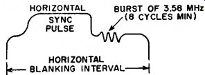
Fig. 96-Waveform for synchronizing signal.
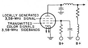
Fig. 97 shows a simplified diagram of a low-level color demodulator
frequently used in color-television receivers. The locally generated
3.58-MHz signal is applied to the grid No. 3 of the pentode. The transmitted
color signal containing the 3.58-MHz side bands is applied to grid No.
1. The phase of the 3.58-MHz color signal constantly changes in accordance
with its color content. For example, the following table shows six variations
in color (hue) as a function of subcarrier phase:
Subcarrier Phase-degrees (with respect to 3.58-MHz local signal in phase with burst) Hue 13 77 119 193 257 299
Yellow Red Magenta Blue Cyan Green
The basic operating principle of the color demodulator shown in Fig. 97 is that plate current from the pentode is zero (or quite low) unless both grid No. 1 and grid No. 3 are simultaneously positive. For example, when the signals applied to the two grids are in phase, plate current can be expected to flow for 180 degrees of each ac cycle. Conversely, when the signals are 180 degrees out of phase, plate current is cut off. The output signal from the detector, therefore, is a function of the phase relationship between the transmitted color signal and the locally generated subcarrier.
In a typical color-television receiver, two color demodulators of the type shown in Fig. 97 are required.

Fig. 97-Low-level color demodulator.
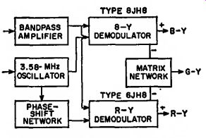
Fig. 98--Block diagram of demodulator circuit used to apply signals
directly to color picture tube.
In one demodulator, the 3.58-MHz subcarrier signal is applied directly to the pentode grid No. 3 from the local "burst" oscillator. In the other demodulator, the 3.58-MHz signal from the burst oscillator is shifted 90 degrees in phase before it is applied to the pentode grid No. 3. As shown previously in Fig. 95, the demodulator B produces R-Y signals. These B-Y and R-Y signals are then combined (matrixed) to produce the G-Y signal, as discussed earlier. The complete luminance signal is then amplified to the required level in a conventional video amplifier circuit.
In some color-television receivers, the demodulators are designed so that the color output signals can be applied directly to the color picture tube. In the diagram shown in Fig. 98, for example, the 6JH8 sheet-beam demodulators produce both positive and negative B-Y and R-Y signals. The positive signals are applied directly to the control grids (grid No. 1) of the blue and red guns of the color picture tube. At the same time, the negative color-difference signals are added (matrixed) in the correct proportions to produce the G-Y signal, which is applied to grid No. 1 of the green gun.
Oscillation
As an oscillator, an electron tube can be employed to generate a continuously alternating voltage. In present day radio broadcast receivers, this application is limited practically to superheterodyne receivers for supplying the heterodyning frequency. Several circuits (represented in Fig. 99) may be utilized, but they all depend on feeding more energy from the plate circuit to the grid circuit than is required to equal the power loss in the grid circuit. Feedback may be produced by electrostatic or electromagnetic coupling between the grid and plate circuits.
When sufficient energy is fed back to more than compensate for the loss in the grid circuit, the tube will oscillate.
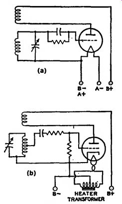
Fig.
99-Tuned-grid triode oscillator circuit: (a) using filament-type tube;
(b) using healer-cathode-type tube.
The action consists of regular surges of power between the plate and the grid circuit at a frequency dependent on the circuit constants of inductance and capacitance. By proper choice of these values, the frequency may be adjusted over a very wide range.
Multivibrators
Relaxation oscillators, which are widely used in present-day electronic equipment, are used to produce non sinusoidal waveshapes such as rectangular and sawtooth pulses. Probably the most common relaxation oscillator is the multivibrator, which may be considered as a two-stage resistance-coupled amplifier in which the output of each tube is coupled into the input of the other tube.
Fig. 100 is a basic multivibrator circuit of the free-running type. In this circuit, oscillations are maintained by the alternate shifting of conduction from one tube to the other. The cycle usually starts with one tube, V1, at zero bias, and the other, V2, at cutoff or beyond.
At this point, the capacitor C1 is charged sufficiently to cut off V2. G then begins to discharge through the resistor R., and the voltage on the grid of V2 rises until V2 begins to conduct. The voltage on the plate of V2 then decreases, causing V1 to conduct less and less. At the same time, the plate voltage of V1 begins to rise, causing V2 to conduct still more heavily.
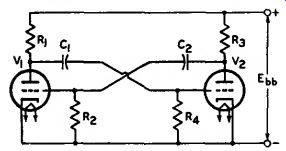
Fig. 100--Basic multivibrator circuit of the free-running type.
Because of the amplification, this cumulative effect builds up extremely fast, and conduction switches from V1 to V2 within a few microseconds, depending on the circuit components.
In this circuit, therefore, conduction switches from V1 to V2 over the interval during which 0 discharges from the voltage across R. to the cutoff voltage for V2 . The actual transfer of conduction does not occur until cutoff is reached. Conduction switches back to V1 through a similar process to complete the cycle. The plate waveform is essentially rectangular in shape, and may be adjusted as to symmetry, frequency, and amplitude by proper choice of circuit constants, tubes, and voltages.
Although this type of multivibrator is free-running, it may be triggered by pulses of a given amplitude and frequency to provide a frequency-stabilized output. Multivibrator circuits may also be designed so that they are not free running, but must be triggered externally to shift conduction from one tube to the other. Depending on the type of circuit, conduction may shift back to the first tube after a given time interval, or the second tube may continue conducting until another trigger signal is applied.
Synchro-guide Circuits
The "synchro-guide" is a controlled type of oscillator used in television receivers to generate and control the synchronized sawtooth voltage necessary for adequate line- or horizontal-frequency scanning. A simplified synchro guide circuit is shown in Fig. 101. This circuit provides stable, noise-free control of a blocking oscillator which generates a horizontal-frequency signal. It permits comparison of the received sync pulses and the generated sawtooth voltages so that properly locked-in horizontal scanning results.
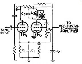
Fig. 101-Simplified synchro-guide circuit.
The triode V2 in Fig. 101 is a conventional blocking oscillator which enables a sawtooth voltage to be developed across the capacitor C2. A portion of this sawtooth is fed back to the grid of the control tube, V1 The positive sync-pulses are also applied to the grid of V1. The waveforms shown in Fig. 102 illustrate the sawtooth and sync pulses (A and B) and their proper "in-sync" combination (C). The sync pulse occurs partly during the portion of the saw tooth voltage in which the triode V, draws current. Any shift in sync pulse as it is superimposed on the sawtooth, therefore, will affect the amount of conduction of the control tube. A change in control-tube conduction ultimately affects the bias on the oscillator tube grid by changing the voltage to which the capacitor G in the cathode circuit may charge. An increase in the positive bias increases the frequency of oscillation.
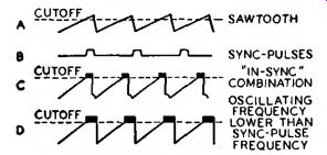
Fig. 102--Sawtooth and sync pulses in synchro-guide circuit.
For example, waveform D in Fig. 102 illustrates a condition in which the sawtooth voltage is advanced in phase with respect to the sync pulses. The widening of the pulse which occurs at the corner of the sawtooth waveform allows the control tube to conduct more current and, consequently, allows the capacitor 0 to charge to a higher voltage. This increased reference voltage also appears in the grid circuit of V2 and makes the grid more positive. The increased grid voltage then speeds up the frequency of oscillations until proper synchronization results.
The blocking oscillator can be made more immune to changes in frequency and noise if Va is brought out of cutoff very sharply. This effect is obtained by sine-wave stabilization. The tuned circuit LaCs in the plate circuit of Fig. 101 superimposes a shock-excited sine wave on the plate and grid waveforms, as shown in Fig. 103.
Automatic Frequency Control
An automatic frequency control (afc) circuit provides a means of correcting automatically the intermediate frequency of a superheterodyne receiver when, for any reason, it drifts from the frequency to which the if stages are tuned. This correction is made by adjusting the frequency of the oscillator.
Such a circuit will automatically compensate for slight changes in rf carrier or oscillator frequency as well as for inaccurate manual or push-button tuning.
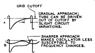
Fig. 103--Waveforms showing effect of tuned circuit L3C3 in Fig. 101.
An afc system requires two sections: a frequency detector and a vari able reactance. The detector section may be essentially the same as the FM detector illustrated in Fig. 30 and discussed under Detection. In the afc system, however, the output is a dc control voltage, the magnitude of which is proportional to the amount of frequency shift. This dc control voltage is used to control the grid bias of an electron tube which comprises the variable reactance section (Fig. 104).
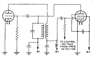
Fig. 104-Automatic-frequency-control (afc) circuit.
The plate current of the reactance tube is shunted across the oscillator tank circuit. Because the plate current and plate voltage of the reactance tube are almost 90 degrees out of phase, the control tube affects the tank circuit in the same manner as a reactance. The grid bias of the tube determines the magnitude of the effective reactance and, consequently, a control of this grid bias can be used to control the oscillator frequency.
Automatic frequency control is also used in television receivers to keep the horizontal oscillator in step with the horizontal-scanning frequency (15,750 Hz) at the transmitter. A widely used horizontal afc circuit is shown in Fig. 105. This circuit, which is often referred to as a balanced-phase-detector or phase-discriminator circuit, is usually employed to control the frequency of a multivibrator-type horizontal-oscillator circuit. The 6AL5 detector supplies a dc control voltage to the grid of the horizontal-oscillator tube which counteracts changes in its operating frequency.
The magnitude and polarity of the control voltages are determined by phase relationships in the afc circuit at a given moment.
The horizontal sync pulses obtained from the sync-separator circuit are fed through a single-triode phase-inverter or phase-splitter circuit to the two diode units of the 6AL5. Because of the action of the phase-inverter circuit, the signals applied to the two diode units are equal in amplitude but 180 degrees out of phase. A reference sawtooth voltage obtained from the horizontal output circuit is also applied simultaneously to both units. Any change in the oscillator frequency alters the phase relationship between the reference sawtooth and the incoming horizontal sync pulses, causing one diode unit of the 6AL5 to con duct more heavily than the other, and thus producing a correction signal. The system remains balanced at all times, therefore, because momentary changes in oscillator frequency are instantaneously corrected by the action of the control voltage.
The diode units of the 6AL5 are biased so that conduction takes place only during the tips of the sync pulses.
The relative position of the sync pulses on the retrace portion of the sawtooth waveform at any given instant determines which diode unit conducts more heavily, and thereby establishes the magnitude and polarity of the control voltage. The network between the diode units and the grid of the horizontal oscillator tube is essentially a low-pass filter which prevents the horizontal sync pulses from affecting the horizontal oscillator performance.
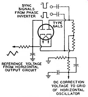
Fig. 105-Balanced phase-detector or phase-discriminator circuit for
horizontal afc.
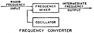
Fig. 106-Block diagram of simple frequency-converter circuit.
Frequency Conversion
Frequency conversion is used in superheterodyne receivers to change the frequency of the rf signal to an inter mediate frequency. To perform this change in frequency, a frequency-converting device consisting of an oscillator and a frequency mixer is employed. In such a device, shown diagrammatically in Fig. 106, two voltages of different frequency, the rf signal voltage and the voltage generated by the oscillator, are applied to the input of the frequency mixer. These voltages beat, or hetero dyne, within the mixer tube to produce a plate current having, in addition to the frequencies of the input voltages, numerous sum and difference frequencies.
The output circuit of the mixer stage is provided with a tuned circuit which is adjusted to select only one beat frequency, i.e., the frequency equal to the difference between the signal frequency and the oscillator frequency The selected output frequency is known as the intermediate frequency, or if.
The output frequency of the mixer tube is kept constant for all values of signal frequency by tuning the oscillator to the proper frequency.
Important advantages gained in a receiver by the conversion of signal frequency to a fixed intermediate frequency are high selectivity with few tuning stages and a high, as well as stable, over all gain for the receiver.
Several methods of frequency con version for superheterodyne receivers are of interest. These methods are alike in that they employ a frequency-mixer tube in which plate current is varied at a combination frequency of the signal frequency and the oscillator frequency.
These variations in plate current produce across the tuned plate load a voltage of the desired intermediate frequency. The methods differ in the types of tubes employed and in the means of supply input voltages to the mixer tube.
A method widely used before the availability of tubes especially designed for frequency-conversion service, and currently used in many FM, television, and standard broadcast receivers, em ploys as mixer tube either a triode, a tetrode, or a pentode, in which oscillator voltage and signal voltage are applied to the same grid. In this method, coupling between the oscillator and mixer circuits is obtained by means of inductance or capacitance.
A second method employs a tube having an oscillator and frequency mixer combined in the same envelope. In one form of such a tube, coupling between the two units is obtained by means of the electron stream within the tube.
Because five grids are used, the tube is called a pentagrid converter.
Grids No. 1 and No. 2 and the cathode are connected to an external circuit to act as a triode oscillator. Grid No. 1 is the grid of the oscillator and grid No. 2 is the anode. Grid No. 2 is connected within the tube to the screen grid (grid No. 4). The combined two grids, Nos. 2 and 4, shield the signal grid (grid No. 3) and act as the composite anode of the oscillator triode. Grid No. 5 acts as the suppressor grid.
Converter tubes of this type are designed so that the space charge around the cathode is unaffected by electrons from the signal grid. Furthermore, the electrostatic field of the signal grid also has little effect on the space charge. The result is that rf voltage on the signal grid produces little effect on the cathode current. There is, therefore, little detuning of the oscillator by avc bias because changes in avc bias produce little change in oscillator transconductance or in the input capacitance of grid No. 1.
Examples of the pentagrid converters discussed in the preceding paragraph are the single-ended types 1R5 and 6BE6. A schematic diagram illustrating the use of the 6BE6 with self excitation is given in Fig. 107. The 6BE6 may also be used with separate excitation. A complete circuit is shown in the Circuits section.
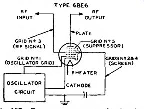
Fig. 107--Frequency-converter circuit using the 6BE6 pentagrid converter
with self excitation.
A further method of frequency conversion employs a tube called a penta grid mixer. This type has two independent control grids and is used with a separate oscillator tube. RF signal voltage is applied to one of the control grids and oscillator voltage is applied to the other. It follows, therefore, that the variations in plate current are due to the combination of the oscillator and signal frequencies.
The tube contains a heater-cathode, five grids, and a plate. Grids Nos. 1 and 3 are control grids. The rf signal voltage is applied to grid No. 1. This grid has a remote-cutoff characteristic and is suited for control by avc bias voltage.
The oscillator voltage is applied to grid No. 3. This grid has a sharp-cutoff characteristic and produces a comparatively large effect on plate current for a small amount of oscillator voltage. Grids Nos. 2 and 4 are connected together within the tube. They accelerate the electron stream and shield grid No. 3 electro statically from the other electrodes.
Grid No. 5, connected within the tube to the cathode, functions similarly to the suppressor grid in a pentode.
In the converter or mixer stage of a television receiver, stable oscillator operation is most readily obtained when separate tubes or tube sections are used for the oscillator and mixer functions.
A typical television mixer-oscillator circuit is shown in Fig. 108. In such circuits, the oscillator voltage is applied to the mixer grid by inductive coupling, capacitive coupling, or a combination of the two. Tubes containing electrically independent oscillator and mixer units in the same envelope, such as the 6EA8 and 6KE8 are designed especially for this application.
OSCILLATOR TUBE OUTPUT MIXER TUBE
Fig. 108--Typical television mixer-oscillator circuit.
Tuning Indication With Electron-Ray Tubes
Electron-ray tubes are designed to indicate visually by means of a fluorescent target the effects of a change in controlling voltage. One application of them is as tuning indicators in radio receivers. Types such as the 6U5 and the 6E5 contain two main parts: (1) a triode which operates as a dc amplifier and (2) an electron-ray indicator which is located in the bulb as shown in Fig. 109. The target is operated at a positive voltage and, therefore, attracts electrons from the cathode. When the electrons strike the target they produce a glow on the fluorescent coating of the tar get. Under these conditions, the target appears as a ring of light.
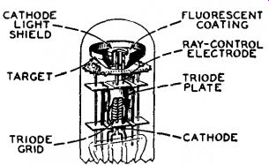
Fig. 109--Structure of electron-ray tube.
A ray-control electrode is mounted between the cathode and target. When the potential of this electrode is less positive than the target, electrons flowing to the target are repelled by the electrostatic field of the electrode, and do not reach that portion of the target behind the electrode. Because the target does not glow where it is shielded from electrons, the control electrode casts a shadow on the glowing target. The extent of this shadow varies from approximately 100 degrees of the target when the control electrode is much more negative than the target to 0 degrees when the control electrode is at approximately the same potential as the target.
In the application of the electron ray tube, the potential of the control electrode is determined by the voltage on the grid of the triode section, as can be seen in Fig. 110. The flow of the triode plate current through resistor R produces a voltage drop which determines the potential of the control electrode. When the voltage of the triode grid changes in the positive direction, plate current increases, the potential of the control electrode goes dawn because of the increased drop across R, and the shadow angle widens. When the potential of the triode grid changes in the negative direction, the shadow angle narrows.
In radio receivers, avc voltage is applied to the grid of the dc amplifier.
Fig. 110--Indicating circuit using an electron-ray tube.
Another type of indicator tube is the 6AF6G. This tube contains only an indicator unit but employs two ray-control electrodes mounted on opposite sides of the cathode and connected to individual base pins. It employs an external dc amplifier. (See Fig. 111.) Thus, two symmetrically opposite shadow angles may be obtained by connecting the two ray-control electrodes together; or, two unlike patterns may be obtained by individual connection of each ray-control electrode to its respective amplifier.
Fig. 111--Indicating circuit using 6AF6G electron-ray tube and external
dc amplifier.
Because avc voltage is at maximum when the set is tuned to give maximum response to a station, the shadow angle is at minimum when the receiver is tuned to resonance with the desired station.
The choice between electron-ray tubes depends on the avc characteristic of the receiver. The 6E5 contains a sharp-cutoff triode which closes the shadow angle on a comparatively low value of avc voltage. The 6U5 has a remote-cutoff triode which closes the shadow on a larger value of avc voltage than the 6E5. The 6AF6G may be used in conjunction with dc amplifier tubes having either remote- or sharp-cutoff characteristics.