THE diversified applications of an electron receiving tube have, within the scope of this section, been treated under seven headings:
Rectification; Detection; Amplification; TV Scanning, Sync, and Deflection; Oscillation: Frequency Conversion; and Tuning Indication with Electron-Ray Tubes.
Although these operations may take place at either radio or audio frequencies and may involve the use of different circuits and different supplemental parts, the general considerations of each kind of operation are basic.
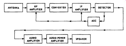
Fig. 14--Simplified block diagram /or a broadcast-band receiver.
General System Functions
When speech, music, or video in formation is transmitted from a radio or television station, the station radiates a modulated radio-frequency (rf) carrier. The function of a radio or television receiver is simply to reproduce the modulating wave from the modulated carrier.
As shown in Fig. 14, a superheterodyne radio receiver picks up the transmitted modulated rf signal, amplifies it, converts it to a modulated intermediate frequency (if) signal, amplifies the modulated if signal, separates the modulating signal from the basic carrier wave (Detection), and amplifies the resulting audio signal to a level sufficient to produce the desired volume in a speaker. In addition, the receiver usually includes some means of producing automatic gain control (age) of the modulated signal before the audio in formation is separated from the carrier.
The transmitted rf signal picked up by the radio receiver may contain either amplitude modulation (AM) or frequency modulation (FM). (These modulation techniques are described later in the section on Detection.) In either case, amplification prior to the detector stage is performed by tuned amplifier circuits designed for the proper frequency and bandwidth. Frequency con version is performed by mixer and oscillator circuits or by a single converter stage which performs both mixer and oscillator functions. Separation of the modulating signal is normally accomplished by one or more diodes in a detector or discriminator circuit. Amplification of the audio signal is then performed by one or more audio amplifier stages.
Audio-amplifier systems for phonograph or tape recordings are similar to the stages after detection in a radio receiver. The input to the amplifier is a low-power-level audio signal from the phonograph or magnetic-tape pickup head. This signal is usually amplified through a preamplifier stage, one or more low-level (pre-driver or driver) audio stages, and an audio power amplifier. The system may also include frequency-selective circuits which act as equalization networks and/ or tone controls.
The operation of a television receiver is more complex than that of a radio receiver, as shown by the simplified block diagram in Fig. 15. The tuner section of the receiver selects the proper rf signals for the desired channel frequency, amplifies them, and converts them to a lower intermediate frequency. As in a radio receiver, these functions are accomplished in rf-amplifier, mixer, and local-oscillator stages. The if signal is then amplified in if-amplifier stages which provide the additional gain required to bring the signal level to an amplitude suitable for detection of the video information.
After detection, the video signal is amplified and separated into sound and picture information. The sound signal is amplified and processed to provide an audio signal which is fed to an audio amplifier system similar to those described above. The picture (video) signal is passed through a video amplifier stage which conveys beam-intensity information to the television picture tube and thus controls instantaneous "spot" brightness. At the same time, deflection circuits cause the electron beam of the picture tube to move the "spot" across the faceplate horizontally and vertically.
Special "sync" signals derived from the video signal assure that the horizontal and vertical scanning are timed so that the picture produced on the receiver exactly duplicates the picture being viewed by the camera or pickup tube.
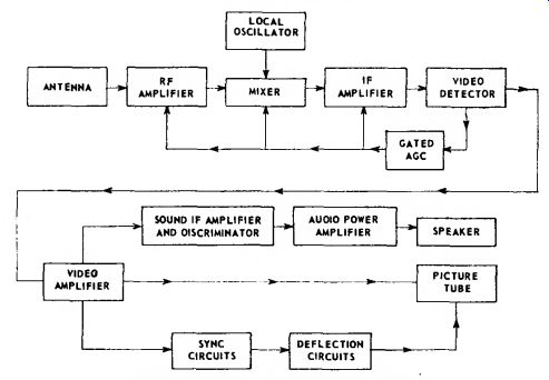
Fig. 15-Simplified block diagram for a black-and-white television receiver.
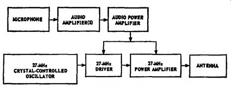
Fig. 16-Simplified block diagram for the transmitter portion of a 27-MHz
communications receiver.
A communications transceiver contains transmitting circuits, as well as receiving circuits similar to those of a radio receiver. The transmitter portion of such a system consists of two sections.
In one section, the desired intelligence (voice, code, or the like) is picked up and amplified through one or more amplifier stages (which are usually common to the receiver portion) to a high level stage called a modulator. In the other section, an rf signal of the desired frequency is developed in an oscillator stage and amplified in one or more rf-amplifier stages. The audio-frequency (af) modulating signal is impressed on the rf carrier in the final rf-power amplifier stage (high-level modulation), in the rf low-level stage (low-level modulation), or in both. Fig. 16 shows a simplified block diagram of the transmitter portion of a citizens-band transceiver that operates at a frequency of 27 MHz (megacycles per second). The transmitting section of a communications system may also include frequency-multiplier circuits which raise the frequency of the developed rf signal as required.
Rectification
The rectifying action of a diode finds important applications in supplying a receiver with dc power from an ac line and in supplying high dc voltage from a high-voltage pulse. A typical arrangement for converting ac to dc includes a rectifier tube, a filter, and a voltage divider. The rectifying action of the tube is explained briefly under Diodes, in the Electrons, Electrodes, and Electron Tubes section. High voltage pulse rectification is described later under Horizontal Output Circuits.
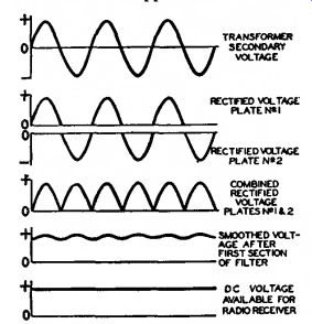
Fig. 17-Voltage waveforms of full-wave rectifier circuit.
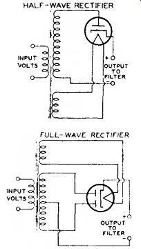
Fig. 18-Half-wave and full-wave rectifier circuits.
The function of a filter is to smooth out the ripple of the tube output, as indicated in Fig. 17, and to increase rectifier efficiency. The action of the filter is explained in the Electron Tube Installation section under Filters.
The voltage divider is used to cut down the output voltage to the values required by the plates and the other electrodes of the tubes in the receiver.
A half-wave rectifier and a full wave rectifier circuit are shown in Fig. 18. In the half-wave circuit, current flows through the rectifier tube to the filter on every other half-cycle of the ac input voltage when the plate is positive with respect to the cathode. In the full wave circuit, current flows to the filter on every half-cycle, through plate No. 1 on one half-cycle when plate No. 1 is positive with respect to the cathode, and through plate No. 2 on the next half-cycle when plate No. 2 is positive with respect to the cathode.
Because the current flow to the filter is more uniform in the full-wave circuit than in the half-wave circuit, the output of the full-wave circuit requires less filtering. Rectifier operating information and circuits are given under each rectifier tube type and in the Circuits section, respectively.
Parallel operation of rectifier tubes furnishes an output current greater than that obtainable with the use of one tube. For example, when two full wave rectifier tubes are connected in parallel, the plates of each tube are connected together and each tube acts as a half-wave rectifier. The permissible voltage and load conditions per tube are the same as for full-wave service but the total load-current handling capability of the complete rectifier is approximately doubled.
When mercury-vapor rectifier tubes are connected in parallel, a stabilizing resistor of 50 to 100 ohms should be connected in series with each plate lead in order that each tube will carry an equal share of the load current. The value of the resistor to be used will depend on the amount of plate current that passes through the rectifier. Low plate current requires a high value; high plate current, a low value. When the plates of mercury-vapor rectifier tubes are connected in parallel, the corresponding filament leads should be similarly connected. Otherwise, the tube drops will be considerably unbalanced and larger stabilizing resistors will be required.
Two or more vacuum rectifier tubes can also be connected in parallel to give correspondingly higher output current and, as a result of paralleling their internal resistances, give some what increased voltage output. With vacuum types, stabilizing resistors may or may not be necessary depending on the tube type and the circuit.
A voltage-doubler circuit of simple form is shown in Fig. 19. The circuit derives its name from the fact that its dc voltage output can be as high as twice the peak value of ac input. Basic ally, a voltage doubter is a rectifier circuit arranged so that the output voltages of two half-wave rectifiers are in series.
The action of a voltage doubler can be described briefly as follows. On the positive half-cycle of the ac input, that is, when the upper side of the ac input line is positive with respect to the lower side, the upper diode passes current and feeds a positive charge into the upper capacitor. As positive charge accumulates on the upper plate of the capacitor, a positive voltage builds up across the capacitor. On the next half-cycle of the ac input, when the upper side of the line is negative with respect to the lower side, the lower diode passes current so that a negative voltage builds up across the lower capacitor.
So long as no current is drawn at the output terminals from the capacitor, each capacitor can charge up to a voltage of magnitude E, the peak value of the ac input. It can be seen from the diagram that with a voltage of +E on one capacitor and -E on the other, the total voltage across the capacitors is 2E. Thus the voltage doubler supplies a no-load dc output voltage twice as large as the peak ac input voltage.
When current is drawn at the output terminals by the load, the output voltage drops below 2E by an amount that depends on the magnitude of the load current and the capacitance of the capacitors. The arrangement shown in Fig. 19 is called a full-wave voltage doubler because each rectifier passes current to the load on each halt of the ac input cycle.
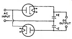
Fig. 19--Full-wave voltage-doubler circuit.
A rectifier type especially designed for use as a voltage doubler is the 25Z6GT. This tube combines two separate diodes in one tube. As a voltage doubler, the tube is used in "transformerless" receivers. In these receivers, the heaters of all tubes in the set are connected in series with a voltage dropping resistor across the line. The connections for the heater supply and the voltage-doubling circuit are shown in Fig. 20.
With the full-wave voltage-doubler circuit in Fig. 20, it will be noted that the dc load circuit cannot be connected to ground or to one side of the ac supply line. This circuit presents certain disadvantages when the heaters of all the tubes in the set are connected in series with a resistance across the ac line.
Such a circuit arrangement may cause hum because of the high ac potential between the heaters and cathodes of the tubes.
The half-wave voltage-doubler circuit in Fig. 20 overcomes this difficulty by making one side of the ac line common with the negative side of the dc load circuit. In this circuit, one half of the tube is used to charge a capacitor which, on the following half cycle, discharges in series with the line voltage through the other half of the tube.
This circuit is called a half-wave voltage doubler because rectified current flows to the load only on alternate halves of the ac' input cycle. The voltage regulation of this arrangement is somewhat poorer than that of the full wave voltage doubler.
Detection

Fig. 20-Full-wave and half-wave voltage-doubler circuits showing heater-supply
connections.

Fig. 21-Waveforms showing effect of amplitude modulation on an rf wove.
When speech, music, or video in formation is transmitted from a radio or television station, the station radiates a radio-frequency (rf) wave which is of either of two general types. In one type, the wave is said to be amplitude modulated when its frequency remains constant and the amplitude is varied.
In the other type, the wave is said to be frequency modulated when its amplitude remains essentially constant but its frequency is varied.
The function of the receiver is to reproduce the original modulating wave from the modulated rf wave. The receiver stage in which this function is performed is called the demodulator or detector stage.
AM Detection
The effect of amplitude modulation on the waveform of the rf wave is shown in Fig. 21. There are three different basic circuits used for the detection of amplitude-modulated waves: the di ode detector, the grid-bias detector, and the grid-resistor detector. These circuits are alike in that they eliminate, either partially or completely, alternate half cycles of the rf wave. With alternate half-cycles removed, the audio variations of the other half-cycles can be amplified to drive headphones or a loud speaker.
A diode-detector circuit is shown in Fig. 22. The action of this circuit when a modulated rf wave is applied is illustrated by Fig. 23. The rf voltage applied to the circuit is shown in light line; the output voltage across capacitor C is shown in heavy line.
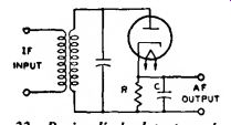
Fig. 22--Basic diode-detector circuit.
Between points (a) and (b) on the first positive half-cycle of the applied rf voltage, capacitor C charges up to the peak value of the rf voltage. Then as the applied rf voltage falls away from its peak value, the capacitor holds the cathode at a potential more positive than the voltage applied to the anode.
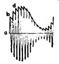
Fig. 23--Waveforms showing modulated rf input (light line) and output
voltage (heavy line) of diode-detector circuit.
The capacitor thus temporarily cuts off current through the diode. While the diode current is cut off, the capacitor discharges from (b) to (c) through the diode load resistor R.
When the rf voltage on the anode rises high enough to exceed the potential at which the capacitor holds the cathode, current flows again and the capacitor charges up to the peak value of the second positive half-cycle at (d). In this way, the voltage across the capacitor follows the peak value of the applied rf voltage and reproduces the AF modulation.
The curve for voltage across the capacitor, as shown in Fig. 23, is some what jagged. However, this jaggedness, which represents an rf component in the voltage across the capacitor, is exaggerated in the drawing. In an actual circuit the rf component of the voltage across the capacitor is negligible. Hence, when the voltage across the capacitor is amplified, the output of the amplifier reproduces the speech or music originating at the transmitting station.
Another way to describe the action of a diode detector is to consider the circuit as a half-wave rectifier. When the rf signal on the plate swings positive, the tube conducts and the rectified current flows through the load resistance R. Because the dc output voltage of a rectifier depends on the voltage of the ac input, the dc voltage across C varies in accordance with the amplitude of the rf carrier and thus reproduces the AF signal. Capacitor C should be large enough to smooth out rf or if variations, but should not be so large as to affect the audio variations. Two diodes can be connected in a circuit similar to a full-wave rectifier to provide full-wave detection. However, in practice, the advantages of this connection generally do not justify the extra circuit complication.
The diode method of detection produces less distortion than other methods because the dynamic characteristics of a diode can be made more linear than those of other detectors.
The disadvantages of a diode are that it does not amplify the signal, and that it draws current from the input circuit and therefore reduces the selectivity of the input circuit. However, because the diode method of detection produces less distortion and because it permits the use of simple avc circuits without the necessity for an additional voltage sup ply, the diode method of detection is most widely used in broadcast receivers.
A typical diode-detector circuit using a diode-triode tube is shown in Fig. 24. Rt is the diode load resistor.
A portion of the AF voltage developed across this resistor is applied to the triode grid through the volume control R3. In a typical circuit, resistor Rt may be tapped so that five-sixths of the total AF voltage across Rt is applied to the volume control. This tapped connection reduces the AF voltage output of the detector circuit slightly, but it reduces audio distortion and improves the rf filtering.
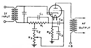
Fig. 24-Typical diode-detector circuit using a twin diode-Mode tube.
DC bias for the triode section is provided by the cathode-bias resistor R2 and the audio bypass capacitor C3. The function of capacitor C2 is to block the dc bias of the cathode from the grid.
The function of capacitor C1 is to by pass any rf voltage on the grid to cathode. A diode-pentode may also be used in this circuit. With a pentode, the AF output should be resistance coupled rather than transformer-coupled.
Another diode-detector circuit, called a diode-biased circuit, is shown in Fig. 25. In this circuit, the triode grid ...
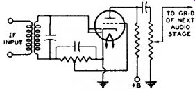
Fig. 25-Diode-biased detector circuit.
... is connected directly to a tap on the diode load resistor. When an rf signal voltage is applied to the diode, the dc voltage at the tap supplies bias to the triode grid. When the rf signal is modulated, the AF voltage at the tap is applied to the grid and is amplified by the triode.
The advantage of the circuit shown in Fig. 25 over the self-biased arrangement shown in Fig. 24 is that the diode-biased circuit does not employ a capacitor between the grid and the diode load resistor, and consequently does not produce as much distortion of a signal having a high percentage of modulation.
However, there are restrictions on the use of the diode-biased circuit. Be cause the bias voltage on the triode depends on the average amplitude of the rf voltage applied to the diode, the average amplitude of the voltage applied to the diode should be constant for all values of signal strength at the antenna. Otherwise there will be different values of bias on the triode grid for different signal strengths and the triode will produce distortion. Because there is no bias applied to the diode biased triode when no rf voltage is applied to the diode, sufficient resistance should be included in the plate circuit of the triode to limit its zero bias plate current to a safe value.
These restrictions mean, in practice, that the receiver should have a separate-channel automatic-volume-control (avc) system. With such an avc system, the average amplitude of the signal voltage applied to the diode can be held within very close limits for all values of signal strength at the antenna.
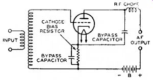
Fig. 26-Grid-bias detector circuit.
The tube used in a diode-biased circuit should be one which operates at a fairly large value of bias voltage. The variations in bias voltage are then a small percentage of the total bias and hence produce small distortion. Tubes taking a fairly large bias voltage are types such as the 6BF6 or 6SR7 having a medium-mu triode. Tube types having a high-mu triode or a pentode should not be used in a diode-biased circuit.
A grid-bias detector circuit is shown in Fig. 26. In this circuit, the grid is biased almost to cutoff, i.e., operated so that the plate current with zero signal is practically zero. The bias voltage can be obtained from a cathode bias resistor, a C-battery, or a bleeder tap. Because of the high negative bias, only the positive half-cycles of the rf signal are amplified by the tube. The signal is, therefore, detected in the plate circuit. The advantages of this method of detection are that it amplifies the signal, besides detecting it, and that it does not draw current from the input circuit and therefore does not reduce the selectivity of the input circuit.
The grid-resistor-and-capacitor method, illustrated in Fig. 27, is somewhat more sensitive than the grid-bias method and gives its best results on weak signals. In this circuit, there is no negative dc bias voltage applied to the grid. Hence, on the positive half-cycles of the rf signal, current flows from grid to cathode. The grid and cathode thus act as a diode detector, with the grid resistor as the diode load resistor and the grid capacitor as the rf bypass capacitor. The voltage across the capacitor then reproduces the AF modulation in the same manner as has been explained for the diode detector. This voltage appears between the grid and cathode and is therefore amplified in the plate circuit. The output voltage thus reproduces the original AF signal.
In this detector circuit, the use of a high-resistance grid resistor increases selectivity and sensitivity. However, improved AF response and stability are obtained with lower values of grid-circuit resistance. This detector circuit amplifies the signal, but draws current from the input circuit and therefore reduces the selectivity of the input circuit.
FM Detection
The effect of frequency modulation on the waveform of the rf wave is shown in Fig. 28. In this type of trans mission, the frequency of the rf wave deviates from a mean value, at an audio frequency rate depending on the modulation, by an amount that is determined in the transmitter and is proportional to the amplitude of the AF modulation signal.
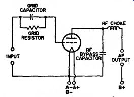
Fig. 27-Detector circuit using grid-resistor and-capacitor bias.
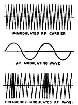
Fig, 28-Waveforms showing effect of frequency modulation on an rf wave.
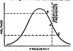
Fig. 29--Resonance curve of a tuned circuit showing desired operating
range for frequency-modulation converter.
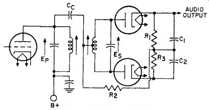
Fig. 30-Balanced phase-shift discriminator circuit.
For this type of modulation, a detector is required to discriminate between deviations above and below the mean frequency and to translate those deviations into a voltage whose amplitude varies at audio frequencies. Since the deviations occur at an audio frequency, the process is one of demodulation, and the degree of frequency deviation determines the amplitude of the demodulated (af) voltage.
A simple circuit for converting frequency variations to amplitude variations is a circuit which is tuned so that the mean radio frequency is on one slope of its resonance characteristic, as at A of Fig. 29. With modulation, the frequency swings between B and C, and the voltage developed across the circuit varies at the modulating rate. In order that no distortion will be introduced in this circuit, the frequency swing must be restricted to the portion of the slope which is effectively straight. Since this portion is very short, the voltage developed is low. Because of these limitations, this circuit is not commonly used but it serves to illustrate the principle.
The faults of the simple circuit are overcome in a push-pull arrangement, such as that shown in Fig. 30, called a balanced phase-shift discriminator. In this detector, the mutually coupled tuned circuits in the primary and secondary windings of the transformer T are tuned to the center frequency. A characteristic of a double-tuned trans former is that the voltages in the primary and secondary windings are 90 degrees out of phase at resonance, and that the phase shift changes as the frequency changes from resonance. Therefore, the signal applied to the diodes and the RC combinations for peak detection also changes with frequency.
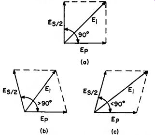
Fig. 31--Diagram illustrating phase shift in double-tuned transformer
(a) at resonance, (b) below resonance, and (c) above resonance.
Because the secondary winding of the transformer T is center-tapped, the applied primary voltage Ep is added to one-half the secondary voltage E, through the capacitor Cc . The addition of these voltages at resonance can be represented by the diagram in Fig. 31(a); the resultant voltage Ei is the signal applied to one peak-detector network consisting of one diode and its RC load.
When the signal frequency decreases (from resonance), the phase shift of E./2 becomes greater than 90 degrees, as shown at (b) in Fig. 31, and E1 be comes smaller. When the signal frequency increases (above resonance), the phase shift of E,/2 is less than 90 degrees as shown at (c), and E1 becomes larger. The curve of E1 as a function of frequency in Fig. 32 is readily identified as the response curve of an FM detector.
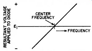
Fig. 32-Diagram showing resultant voltage E1 in Fig. 31 as a function
of frequency.
Because the discriminator circuit shown in Fig. 30 uses a push-pull con figuration, the diodes conduct on alternate half-cycles of the signal frequency and produce a plus-and-minus output with respect to zero rather than with respect to E1. The primary advantage of this arrangement is that there is no output at resonance. When an FM signal is applied to the input, the audio output voltage varies above and below zero as the instantaneous frequency varies above and below resonance. The frequency of this audio voltage is determined by the modulation frequency of the FM signal, and the amplitude of the voltage is proportional to the frequency excursion from resonance. (The resistor R2 in the circuit provides a dc return for the diodes, and also maintains a load impedance across the primary winding of the transformer.) One disadvantage of the balanced phase-shift discriminator shown in Fig. 30 is that it detects audio modulation (AM) as well as frequency modulation (FM) in the if signal because the circuit is balanced only at the center frequency. At frequencies off resonance, any variation in amplitude of the if signal is reproduced to some extent in the audio output.
The ratio-detector circuit shown in Fig. 33 is a discriminator circuit which has the advantage of being relatively insensitive to amplitude variations in the FM signal. In this circuit, EP is added to E./2 through the mutual coupling M. (this voltage addition may be made by either mutual or capacitive coupling). Because of the phase-shift relationship of these voltages, the resultant detected signals vary with frequency variations in the same manner as described for the phase-shift discriminator circuit shown in Fig. 30. However, the diodes in the ratio detector are placed "back-to-back" (in series, rather than in push-pull) so that both halves of the circuit operate simultaneously during one-half of the signal frequency cycle (and are cut off on the other half cycle). As a result, the detected voltages E1 and E2 are in series, as shown for the instantaneous polarities that occur during the conduction half-cycle. When the audio output is taken between the equal capacitors C1 and C2, there fore, the output voltage is equal to (E2-E1)/2 (for equal resistors R1 and R2 ).
The dc circuit of the ratio detector consists of a path through the secondary winding of the transformer, both diodes (which are in series), and resistors R1 and R.. The value of the electrolytic capacitor C> is selected so that the time constant of R1, Rs, and C» is very long compared to the detected audio signal.
As a result, the sum of the detected voltages (E1 + Es) is a constant and the AM components on the signal frequency are suppressed. This feature of the ratio detector provides improved AM rejection as compared to the phase-shift discriminator circuit shown in Fig. 30.
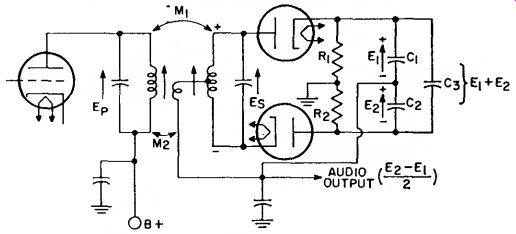
Fig. 33--Ratio-detector circuit.
Amplification
The amplifying action of an electron tube was mentioned under Triodes in the section on Electrons, Electrodes, and Electron Tubes. This action can be utilized in electronic circuits in a number of ways, depending upon the results desired. Four classes of amplifier service recognized by engineers are covered by definitions standardized by the Institute of Electrical and Electronics Engineers. This classification depends primarily on the fraction of input cycle during which plate current is expected to flow under-rated full-load conditions. The classes are class A, class AB, class B, and class C.
The term "cutoff bias" used in these definitions is the value of grid bias at which plate current is very small (i.e., approaches zero).
Classes of Service
A class A amplifier is an amplifier in which the grid bias and alternating grid voltages are such that plate current in a specific tube flows at all times.
A class AB amplifier is an amplifier in which the grid bias and alternating grid voltages are such that plate current in a specific tube flows for appreciably more than half but less than the entire electrical cycle.
A class B amplifier is an amplifier in which the grid bias is approximately equal to the cutoff value, so that the plate current is approximately zero when no exciting grid voltage is applied, and so that plate current in a specific tube flows for approximately one-half of each cycle when an alternating grid voltage is applied.
A class C amplifier is an amplifier in which the grid bias is appreciably greater than the cutoff value, so that the plate current in each tube is zero when no alternating grid voltage is applied, and so that plate current flows in a specific tube for appreciably less than one-half of each cycle when an alternating grid voltage is applied.
The suffix 1 may be added to the letter or letters of the class identification to denote that grid current does not flow during any part of the input cycle. The suffix 2 may be used to denote that grid current flows during part of the cycle.
For radio-frequency (rf) amplifiers which operate into a selective tuned circuit, as in radio transmitter applications, or under requirements where distortion is not an important factor, any of the above classes of amplifiers may be used, either with a single tube or with a push-pull stage. For audio frequency (af) amplifiers in which distortion is an important factor, only class A amplifiers permit single-tube operation. In this case, operating conditions are usually chosen so that distortion is kept below the conventional 5 percent for triodes and the conventional 7 to 10 percent for tetrodes or pentodes. Distortion can be reduced below these figures by means of special circuit arrangements such as that discussed under inverse feedback. With class A amplifiers, reduced distortion with improved power performance can be obtained by using a push-pull stage for audio service. With class AB and class B amplifiers, a balanced stage using two tubes is required for audio service.
Class A Voltage Amplifiers
As a class A voltage amplifier, an electron tube is used to reproduce grid voltage variations across an impedance or a resistance in the plate circuit.
These variations are essentially of the same form as the input signal voltage impressed on the grid, but their amplitude is increased. This increase is accomplished by operation of the tube at a suitable grid bias so that the applied grid input voltage produces plate-current variations proportional to the signal swings. Because the voltage variation obtained in the plate circuit is much larger than that required to swing the grid, amplification of the signal is obtained.
Fig. 34 gives a graphical illustration of this method of amplification and shows, by means of the grid-voltage vs. plate-current characteristics curve, the effect of an input signal (S) applied to the grid of a tube. The output signal (O) is the resulting amplified plate-current variation.
The plate current flowing through the load resistance (R) of Fig. 35 causes a voltage drop which varies directly with the plate current. The ratio of this voltage variation produced in the load resistance to the input signal voltage is the voltage amplification, or gain, provided by the tube. The voltage amplification due to the tube is expressed by the following convenient formulas:
Voltage amplification - -
Ki. + rp gm X fp X R1
0r 1000000 X (rp + R1)
… where n is the amplification factor of the tube, R1 is the load resistance in ohms, rp is the plate resistance in ohms, and gm is the transconductance in micro-mhos.
From the first formula, it can be seen that the gain actually obtainable from the tube is less than the tube amplification factor, but that the gain approaches the amplification factor when the load resistance is large compared to the tube plate resistance. Fig. 36 shows graphically how the gain approaches the amplification factor of the tube as the load resistance is increased.
From the curve it can be seen that a high value of load resistance should be used to obtain high gain in a voltage amplifier.
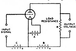
Fig. 35-Triode amplifier circuit.
In a resistance-coupled amplifier, the load resistance of the tube is approximately equal to the resistance of the plate resistor in parallel with the grid resistor of the following stage.
Hence, to obtain a large value of load resistance, it is necessary to use a plate resistor and a grid resistor of large resistance. However, the plate resistor should not be too large because the flow of plate current through the plate resistor produces a voltage drop which reduces the plate voltage applied to the tube. If the plate resistor is too large, this drop will be too large, the plate voltage on the tube will be too small, and the voltage output of the tube will be too small. Also, the grid resistor of the following stage should not be too large, the actual maximum value being dependent on the particular tube type. This precaution is necessary be cause all tubes contain minute amounts of residual gas which cause a minute flow of current through the grid resistor.
If the grid resistor is too large, the positive bias developed by the flow of this current through the resistor decreases the normal negative bias and produces an increase in the plate current. This increased current may overheat the tube and cause liberation of more gas which, in turn, will cause further decrease in bias. The action is cumulative and results in a runaway condition which can destroy the tube.
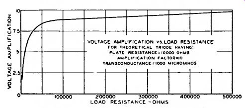
Fig. 36--Gain curve for triode amplifier circuit.
A higher value of grid resistance is permissible when cathode-resistor bias is used than when fixed bias is used. When cathode-resistor bias is used, a loss in bias due to gas or grid-emission effects is almost completely offset by an increase in bias due to the voltage drop across the cathode resistor. Typical values of plate resistor and grid resistor for tube types used in resistance-coupled circuits, and the values of gain obtain able, are shown in the Resistance Coupled Amplifier section.
The input impedance of an electron tube (that is, the impedance between grid and cathode) consists of (1) a reactive component due to the capacitance between grid and cathode, (2) a resistive component resulting from the time of transit of electrons between cathode and grid, and (3) a resistive component developed by the part of the cathode lead inductance which is common to both the input and output circuits. These components are dependent on the frequency of the in coming signal. The input impedance is very high at audio frequencies when a tube is operated with its grid biased negative. In a class A1 or AB1 transformer-coupled audio amplifier, there fore, the loading imposed by the grid on the input transformer is negligible.
As a result, the secondary impedance of a class A1 or class AB1 input trans former can be made very high because the choice is not limited by the input impedance of the tube; however, trans former design considerations may limit the choice.
At the higher radio frequencies, the input impedance may become very low even when the grid is negative, due to the finite time of passage of electrons between cathode and grid and to the appreciable lead reactance. This impedance drops very rapidly as the frequency is raised, and increases input circuit loading. In fact, the input impedance may become low enough at very high radio frequencies to affect the gain and selectivity of a preceding stage appreciably. Tubes such as the "acorn" and "pencil" types and the high-frequency miniatures have been developed to have low input capacitances, low electron-transit time, and low lead inductance so that their input impedance is high even at the ultra high radio frequencies. Input admittance is the reciprocal of input impedance.
A remote-cutoff amplifier tube is a modified construction of a pentode or a tetrode type designed to reduce modulation-distortion and cross-modulation in radio-frequency stages. Cross modulation is the effect produced in a radio or television receiver by an interfering station "riding through" on the carrier of the station to which the receiver is tuned. Modulation-distortion is a distortion of the modulated carrier and appears as audio-frequency distortion in the output. This effect is produced by a radio-frequency amplifier stage operating on an excessively curved characteristic when the grid bias has been increased to reduce volume. The offending stage for cross-modulation is usually the first radio-frequency amplifier, while for modulation-distortion the cause is usually the last intermediate-frequency stage. The characteristics of remote-cutoff types are such as to enable them to handle both large and small input signals with minimum distortion over a wide range of signal strength.
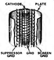
Fig. 37-Structure of remote-cutoff grid.
Fig. 37 illustrates the construction of the grid No. 1 (control grid) in a remote-cutoff tube. The remote-cutoff action is due to the structure of the grid which provides a variation in amplification factor with change in grid bias. The grid No. 1 is wound with open spacing at the middle and with close spacing at the ends. When weak signals and low grid bias are applied to the tube, the effect of the non-uniform turn spacing of the grid on cathode emission and tube characteristics is essentially the same as for uniform spacing. As the grid bias is made more negative to handle larger input signals, the electron flow from the sections of the cathode enclosed by the ends of the grid is cut off. The plate current and other tube characteristics are then dependent on the electron flow through the open section of the grid. This action changes the gain of the tube so that large signals may be handled with minimum distortion due to cross-modulation and modulation-distortion.
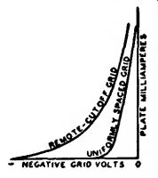
Fig. 38-Plate-current curves for triodes having remote-cutoff and uniformly
spaced grids.
Fig. 38 shows a typical plate-current vs. grid-voltage curve for a remote cutoff type compared with the curve for a type having a uniformly spaced grid. It will be noted that while the curves are similar at small grid-bias voltages, the plate current of the remote-cutoff tube drops quite slowly with large values of bias voltage. This slow change makes it possible for the tube to handle large signals satisfactorily. Because remote-cutoff types can accommodate large and small signals, they are particularly suitable for use in sets having automatic volume control. Remote-cutoff tubes also are known as variable-mu types.
Class A Power Amplifiers
As a class A power amplifier, an electron tube is used in the output stage of a radio or television receiver to sup ply a relatively large amount of power to the loudspeaker. For this application, large power output is of more importance than high voltage amplification; therefore, gain possibilities are sacrificed in the design of power tubes to obtain power-handling capability.
Triodes, pentodes, and beam power tubes designed for power amplifier service have certain inherent features for each structure. Power tubes of the triode type for class A service are characterized by low power sensitivity, low plate-power efficiency, and low distortion. Power tubes of the pentode type are characterized by high power sensitivity, high plate-power efficiency and, usually, somewhat higher distortion than class A triodes. Beam power tubes have higher power sensitivity and efficiency than triode or conventional pentode types.
A class A power amplifier is also used as a driver to supply power to a class AB2 or a class B stage. It is usually advisable to use a triode, rather than a pentode, in a driver stage be cause of the lower plate impedance of the triode.
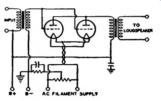
Fig. 39--Power amplifier with tubes connected in parallel.
Power tubes connected in either parallel or push-pull may be employed as class A amplifiers to obtain increased output. The parallel connection (Fig. 39) provides twice the output of a single tube with the same value of grid signal voltage. With this connection, the effective transconductance of the stage is doubled, and the effective plate resistance and the load resistance required are halved as compared with single-tube values.
The push-pull connection (Fig. 40), although it requires twice the grid signal voltage, provides increased power and has other important advantages over single-tube operation. Distortion caused by even-order harmonics and hum caused by plate-voltage-supply fluctuations are either eliminated or decidedly reduced through cancellation.
Because distortion for push-pull operation is less than for single-tube operation, appreciably more than twice single-tube output can be obtained with triodes by decreasing the load resistance for the stage to a value approaching the load resistance for a single tube.
For either parallel or push-pull class A operation of two tubes, all electrode currents are doubled while all dc electrode voltages remain the same as for single-tube operation. If a cathode resistor is used, its value should be about one-half that for a single tube.
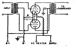
Fig. 40--Power amplifier with lubes connected in push-pull.
If oscillations occur with either type of connection, they can often be eliminated by the use of a non-inductive resistor of approximately 100 ohms connected in series with each grid at the socket terminal.
Operation of power tubes so that the grids run positive is inadvisable except under conditions such as those discussed in this section for class AB and class B amplifiers.
Power-Output Calculations
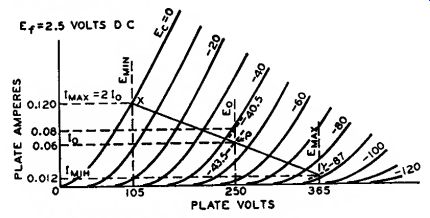
Fig. 41—Graphic calculations for class A amplifier using a power triode.
Calculation of the power output of a triode used as a class A amplifier with either an output transformer or a choke having low dc resistance can be made without serious error from the plate family of curves by assuming a resistance load. The proper plate current, grid bias, optimum load resistance, and per-cent second-harmonic distortion can also be determined. The calculations are made graphically and are illustrated in Fig. 41 for given conditions. The procedure is as follows:
(1) Locate the zero-signal bias point P by determining the zero-signal bias Eco from the formula:
Zero-signal bias (Eco) -(0.68 X Eb)//i
…. where Eb is the chosen value in volts of dc plate voltage at which the tube is to be operated, and p is the amplification factor of the tube. This quantity is shown as negative to indicate that a negative bias is used.
(2) Locate the value of zero-signal plate current, Io, corresponding to point P.
(3) Locate the point 2Io, which is twice the value of I„ and corresponds to the value of the maximum-signal plate current Imax.
(4) Locate the point X on the dc bias curve at zero volts, Ec = 0, corresponding to the value of I ..,.
(5) Draw a straight line XY through X and P.
Line XY is known as the load resistance line. Its slope corresponds to the value of the load resistance. The load resistance in ohms is equal to (E.„ - Emu) divided by (Im.i - In.), where E is in volts and I is in amperes.
It should be noted that in the case of filament types of tubes, the calculations are given on the basis of a dc operated filament. When the filament is ac-operated, the calculated value of dc bias should be increased by approximately one-half the filament voltage rating of the tube.
The value of zero-signal plate current Io should be used to determine the plate dissipation, an important factor influencing tube life. In a class A amplifier under zero-signal conditions, the plate dissipation is equal to the power input, i.e., the product of the dc plate voltage Eo and the zero-signal dc plate current L. If it is found that the plate dissipation rating of the tube is exceeded with the zero-signal bias Eco calculated above, it will be necessary to increase the bias by a sufficient amount so that the actual plate dissipation does not exceed the rating before proceeding further with the remaining calculations.
For power-output calculations, it is assumed that the peak alternating grid voltage is sufficient (1) to swing the grid from the zero-signal bias value Eco to zero bias (Ec = 0) on the positive swing and (2) to swing the grid to a value twice the zero-signal bias value on the negative swing. During the negative swing, the plate voltage and plate current reach values of Emax and Imu; during the positive swing, they reach values of Emm and Im»- Because power is the product of voltage and current, -the power output P0 as shown by a watt-meter is given by:
P. = (ImftS-Imln) X (Emu-Emlp) where E is in volts, I is in amperes, and P. is in watts.
In the output of power-amplifier triodes, some distortion is present. This distortion is due predominantly to second harmonics in single-tube amplifiers.
The percentage of second-harmonic distortion may be calculated by the following formula:
Im«« -fr" Im In
-Io
% distortion = s ; X 100 Imix – im
In where L is the zero-signal plate current in amperes. If the distortion is excessive, the load resistance should be increased or, occasionally, decreased slightly and the calculations repeated.
Example: Determine the load resistance, power output, and distortion of a triode having an amplification factor of 4.2, a plate-dissipation rating of 15 watts, and plate-characteristics curves as shown in Fig. 41. The tube is to be operated at 250 volts on the plate.
Procedure: For a first approximation, determine the operating point P from the zero-signal bias formula, Ea> = -(0.68 X 250) /4.2 = -40.5 volts.
From the curve for this voltage, it is found that the zero-signal plate current is 0.08 ampere and, therefore, the plate dissipation rating is exceeded (0.08 X 250 = 20 watts). Consequently, it is necessary to reduce the zero-signal plate current to 0.06 ampere at 250 volts. The grid bias is then -43.5 volts.
Note that the curve was taken with a dc filament supply; if the filament is to be operated on an ac supply, the bias must be increased by about one half the filament voltage, or to -45 volts, and the circuit returns made to the mid-point of the filament circuit.
Point X can then be determined.
Point X is at the intersection of the dc bias curve at zero volts with Im«, where Im.r = 2I„ = 2 X 0.06 = 0.12 ampere.
Line XY is drawn through points P and X. Emax* E_min, and I_min are then found from the curves. When these values are substituted in the power-output formula, the following result is obtained:
P. = (012 - 0.012) X (365 -105) =^^ The resistance represented by load line XY is (365 - 105) (0.12 - 0.012) - 2410 ohms
When the values from the curves are substituted in the distortion formula, the following result is obtained:
0.12 + 0.012
-0.06
% distortion =
0.12 - 0.012
-X 100 = 5.5%
It is customary to select the load resistance so that the distortion does not exceed five percent When the method shown is used to determine the slope of the load-resistance line, the second-harmonic distortion generally does not exceed five percent. In the example, however, the distortion is excessive and it is desirable, therefore, to use a slightly higher load resistance. A load resistance of 2500 ohms will provide a distortion of about 4.9 percent. The power output is reduced only slightly to 3.5 watts.
Operating conditions for Modes in push-pull depend on the type of operation desired. Under class A conditions, distortion, power output, and efficiency are all relatively low. The operating bias can be anywhere between that specified for single-tube operation and that equal to one-half the grid-bias voltage required to produce plate-current cutoff at a plate voltage of 1.4E0 , where E„ is the operating plate voltage. Higher bias than this value requires higher grid signal voltage and results in class AB1 operation, which is discussed later.
The method for calculating maximum power output for triodes in push pull class A operation is as follows:
Erect a vertical line at 0.6 E„ (see Fig. 42), intersecting the Ec - 0 curve at the point Ira.x. Then, Im, x is determined from the curve for use in the formula Po= (In,.. XEo)/5
If I mix is expressed in amperes and E0 in volts, power output is in watts.
The method for determining the proper load resistance for triodes in push-pull is as follows: Draw a load line through I m„ on the zero-bias curve and through the E„ point on the zero-current axis. Four times the resistance represented by this load line is the plate-to plate load (RpP) for two triodes in a class A push-pull amplifier. Expressed as a formula, RPP = 4 X (Eo - 0.6Eo)/Im«« where E„ is expressed in volts, Im«x in amperes, and Rpp in ohms.
Example:
Assume that the plate voltage (E„) is to be 300 volts, and the plate-dissipation rating of the tube is 15 watts. Then, for class A operation, the operating bias can be equal to, but not more than, one-half the grid bias for cutoff with a plate voltage of 1.4 x 300 = 420 volts.
(Since cutoff bias is approximately - 115 volts at a plate voltage of 420 volts, one-half of this value is -57.5 volts bias.)
At this bias, the plate current is found from the plate family to be 0.054 ampere and, there fore, the plate dissipation is 0.054 x 300 or 16.2 watts. Since -57.5 volts is the limit of bias for class A operation of these tubes at a plate voltage of 300 volts, the dissipation cannot be reduced by increasing the bias and it becomes necessary to reduce the plate voltage.
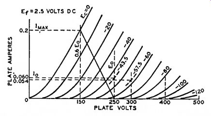
Fig. 42-Graphic calculations for push-pull class A amplifier using a
power Mode.
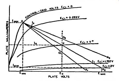
Fig. 43-Graphic calculations for class A amplifier using a pentode or
beam power tube.
If the plate voltage is reduced to 250 volts, the bias will be found to be -43.5 volts. For this value, the plate current is 0.06 ampere, and the plate dissipation is 15 watts. Then, following the method for calculating power output, erect a vertical line at 0.6Eo = 150 volts.
The intersection of thp line wi volts.
The intersection of the line with the curve Ec = 0 is I msl or 0.2 ampere.
When this value is substituted in the power formula, the power output is (0.2 x 250)/ 5 = 10 watts. The load resistance is determined from the load formula:
Plate-to-plate load (Rpp) = 4 X (250 - 150)/0.2 = 2000 ohms.
Power output for a pentode or a beam power rube as a class A amplifier can be calculated in much the same way as for triodes. Calculations can be made graphically from a special plate family of curves, as shown in Fig. 43.
From a point A at or just below the knee of the zero-bias curve, draw arbitrarily selected load lines to inter sect the zero-plate-current axis. These lines should be on both sides of the operating point P, whose position is determined by the desired operating plate voltage, E0, and one-half the maximum-signal plate current. Along any load line, say AA1, measure the distance AO2. On the same line, lay off an equal distance, 01A1. For optimum operation, the change in bias from A to Oi should be nearly equal to the change in bias from 01 to A1. If this condition can not be met with one line, as is the case for the line first chosen, then another should be chosen. When the most satisfactory line has been selected, its resistance may be determined by the following formula:
Load resistance
(R_L) = - Em In
- Imln
The value of R1 may then be substituted in the following formula for calculating power output
P„ = [In... - Imln + 1.41 (Ii - I; ) ]* Rl 32
In both of these formulas, I is in amperes, E is in volts, R_L is in ohms, and P. is in watts. I, and IT are the current values on the load line at bias voltages of Ec, = V - 0.707V = 0.293V and E.i = V + 0.707V = 1.707V, respectively.
Calculations for distortion may be made by means of the following formulas. The terms used have already been defined.
> 2nd-harmonic distortion =
Im.i -f- Imln - 2 Io X 100 X 100
- Imln + 1.41 (Ix - Ijr)
% 3rd-harmonic distortion :
- Imln - 1.41 (I« - IT ) Im.i - Imln + 1.41 (Ii - I,)
% total (2nd and 3rd) harmonic distortion =
V(% 2nd)»+ (% 3rd)'
Conversion Factors
Operating conditions for voltage values other than those shown in the published data can be obtained by use of the nomograph shown in Fig. 44 when all electrode voltages are changed simultaneously in the same ratio. The nomograph includes conversion factors for current (Fi), power output (F,), plate resistance or load resistance (Fr).
and transconductance (F»m) for voltage ratios between 0.5 and 2.0. These factors are expressed as functions of the ratio between the desired or new voltage for any electrode (Ed..) and the published or original value of that voltage (Epub). The relations shown are applicable to triodes and multigrid tubes in all classes of service.
To use the nomograph, simply place a straight-edge across the page so that it intersects the scales for Ed., and Ep»b at the desired values. The desired conversion factor may then be read directly or estimated at the point where the straight-edge intersects the Fi, F, Fr , or F«„ scale.
For example, suppose it is desired to operate two 6L6GC's in class A1 push-pull, fixed bias, with a plate voltage of 200 volts. The nearest published operating conditions for this class of service are for a plate voltage of 250 volts. The operating conditions for the new plate voltage can be determined as follows:
The voltage conversion factor, F., is equal to 200/250 or 0.8. The dashed lines on the nomograph of Fig. 44 indicate that for this voltage ratio Fi is approximately 0.72, Fp is approximately 0.57, Fr is 1.12, and F_gm is approximately 0.892. These factors may be applied directly to operating values shown in the tube data, or to values calculated by the methods described previously.
Because this method for conversion of characteristics is necessarily an approximation, the accuracy of the nomograph decreases progressively as the ratio Ede./Epub departs from unity. In general, results are substantially correct when the value of the ratio Ej../Ep„b is between 0.7 and 1.5. Beyond these limits, the accuracy decreases rapidly, and the results obtained must be considered rough approximations.
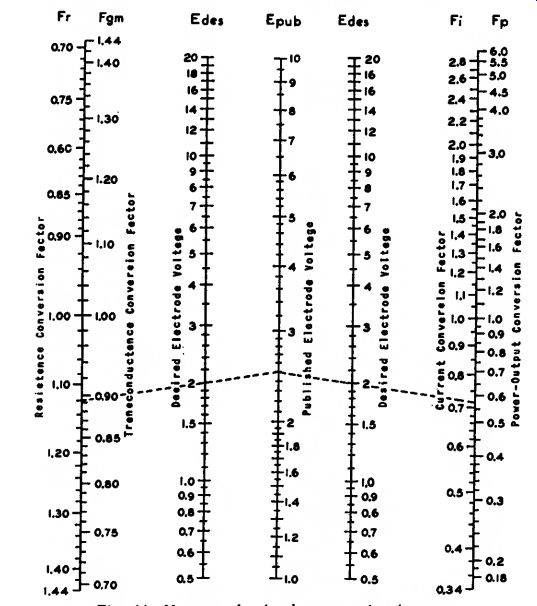
Fig. 44--Nomograph of tube conversion factors.
The nomograph does not take into consideration the effects of contact potential or secondary emission in tubes.
Because contact-potential effects be come noticeable only at very small dc grid-No. 1 (bias) voltages, they are generally negligible in power tubes.
Secondary emission may occur in conventional tetrodes, however, if the plate voltage swings below the grid-No. 2 voltage. Consequently, the conversion factors shown in the nomograph apply to such tubes only when the plate voltage is greater than the grid-No. 2 voltage. Because secondary emission may also occur in certain beam power tubes at very low values of plate current and plate voltage, the conversion factors shown in the nomograph do not apply when these tubes are operated under such conditions.
Class AB Power Amplifiers
A class AB power amplifier em ploys two tubes connected in push-pull with a higher negative grid bias than is used in a class A stage. With this higher negative bias, the plate and screen grid voltages can usually be made higher than for class A amplifiers be cause the increased negative bias holds plate current within the limit of the tube plate-dissipation rating. As a result of these higher voltages, more power output can be obtained from class AB operation.
Class AB amplifiers are subdivided into class AB, and class AB2. In class AB1, there is no flow of grid current.
That is, the peak signal voltage applied to each grid is not greater than the negative grid-bias voltage. The grids therefore are not driven to a positive potential and do not draw current. In class AB: , the peak signal voltage is greater than the bias so that the grids are driven positive and draw current.
Because of the flow of grid current in a class AB, stage, there is a loss of power in the grid circuit. The sum of this loss and the loss in the input trans former is the total driving power required by the grid circuit. The driver stage should be capable of a power output considerably larger than this required power in order that distortion introduced in the grid circuit be kept low. The input transformer used in a class AB. amplifier usually has a step down turns ratio.
Because of the large fluctuations of plate current in a class AB* stage, it is important that the plate power supply have good regulation. Otherwise the fluctuations in plate current cause fluctuations in the voltage output of the power supply, with the result that power output is decreased and distortion is increased. To obtain satisfactory regulation, it is usually advisable to use a low-drop rectifier, such as the 5V4GA, with a choke-input filter. In all cases, the resistance of the choke and trans formers should be as low as possible
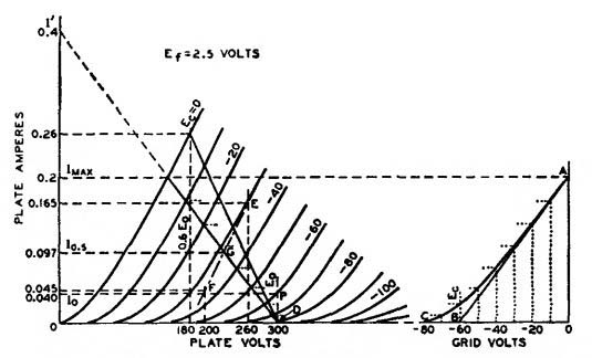
Fig. 45--Graphic calculations for class AB, amplifier F using a power
triode.
Fig. 46--Instantaneous curve for class AB, amplifier.
Class AB1 Power Amplifiers In class AB1 push-pull amplifier service using triodes, the operating conditions may be determined graphically by means of the plate family if Eo, the desired operating plate voltage, is given. In this service, the dynamic load line does not pass through the operating point P as in the case of the single-tube amplifier, but through the point D in Fig. 45. Its position is not affected by the operating grid bias provided the plate-to-plate load resistance remains constant.
Under these conditions, grid bias has no appreciable effect on the power output. Grid bias cannot be neglected, however, since it is used to find the zero-signal plate current and, from it, the zero-signal plate dissipation. Be cause the grid bias is higher in class AB1 than in class A service for the same plate voltage, a higher signal voltage may be used without grid current being drawn and, therefore, higher power output is obtained.
In general, for any load line through point D, Fig. 45, the plate-to plate load resistance in ohms of a push pull amplifier is:
Rp, = 4Eo/I', where I' is the plate-current value in amperes at which the load line as projected intersects the plate-current axis, and E, is in volts. This formula is an other form of the one given under push pull class A amplifiers, Rpp = 4(Eo - 0.6E„)/Im«I, but is more general.
Power output = (Im.x/V^)' X Rp»/4,
... where Im.r is the peak plate current at zero grid volts for the load chosen. This formula simplified is (In..*) 5 X Rpp /8.
The maximum-signal average plate current is 2Imu/ir or 0.636 the maximum-signal average power input is
0.636 I„„ X Eo.
It is desirable to simplify these formulas for a first approximation. This simplification can be made if it is assumed that the peak plate current, Im.i, occurs at the point of the zero-bias curve corresponding approximately to 0.6 Eo, the condition for maximum power output. The simplified formulas are:
Po (for two tubes) = (Im.i X Eo)/5 Rpp = 1.6Eo/Imax
... where Eo is in volts, Im.x is in amperes, Rpp is in ohms, and P» is in watts.
It may be found during subsequent calculations that the distortion or the plate dissipation is excessive for this approximation; in that case, a different load resistance must be selected, using the first approximation as a guide, and the process repeated to obtain satisfactory operating conditions.
Example: Fig. 45 illustrates the application of this method to a pair of power triodes operated at E„ = 300 volts. Each tube has a plate-dissipation rating of 15 watts. The method is to erect a vertical line at 0.6E_o, or at 180 volts, which intersects the E« = 0 curve at the point Im.« = 0.26 ampere. Using the simplified formulas, the following values are obtained: (0.26 X 300)/5 = 15.6 watts
At this point, it is well to determine the plate dissipation and to compare it with the maximum rated value.
From the average-plate-current formula (0.636 Im.x) mentioned previously, the maximum-signal average plate current is 0.166 ampere. The product of this current and the operating plate voltage is 49.8 watts, the average input to the two tubes. From this value, subtract the power output of 15.6 watts to obtain the total dissipation for both tubes, which is 34.2 watts. Half of this value, 17 watts, is in excess of the 15-watt rating of the tube and it is necessary, therefore, to assume another and higher load resistance so that the plate-dissipation rating will not be exceeded.
It will be found that at an operating plate voltage of 300 volts the tubes require a plate-to-plate load resistance of 3000 ohms. From the formula for RPP, the value of I' is found to be 0.4 ampere. The load line for the 3000 ohm load resistance is then represented by a straight line from the point I' = 0.4 ampere on the plate-current ordinate to the point E„ = 300 volts on the plate-voltage abscissa. At the inter section of the load line with the zero bias curve, the peak plate current, lm.«, can be read at 0.2 ampere.
Then Po = (Im.i/ V2)2 X Rpp/4
= (0.2/1.41) 2 X 3000/4
= 15 watts
Proceeding as in the first approximation, it is found that the maximum signal average plate current, 0.636Im«x, is 0.127 ampere, and the maximum signal average power input is 38.1 watts.
This input minus the power output is 38.1 - 15 = 23.1 watts. This value is the dissipation for two tubes; the value per tube is 11.6 watts, a value well within the rating of this tube type.
The operating bias and the zero signal plate current may then be found by use of a curve which is derived from the plate family and the load line. Fig. 46 is a curve of instantaneous values of plate current and dc grid-bias voltages taken from Fig. 45. Values of grid bias are read from each of the grid-bias curves of Fig. 45 along the load line and are transferred to Fig. 46 to produce the curved line from A to C. A tangent to this curve, starting at A, is drawn to intersect the grid-voltage abscissa. The point of intersection, B, is the operating grid bias for fixed-bias operation. In the example, the bias is -60 volts. Refer back to the plate family at the operating conditions of plate volts = 300 and grid bias = -60 volts; the zero-signal plate current per tube is seen to be 0.04 ampere.
This procedure locates the operating point for each tube at P. The plate current must be doubled, of course, to obtain the zero-signal plate current for both tubes. Under maximum-signal conditions, the signal voltage swings from zero-signal bias voltage to zero bias for each tube on alternate half cycles.
Hence, in the example, the peak of signal voltage per tube is 60 volts, or the grid-to-grid value is 120 volts.
As in the case of the push-pull class A amplifier, the second-harmonic distortion in a class AB! amplifier using triodes is very small and is largely canceled by virtue of the push-pull connection. Third-harmonic distortion, however, which may be larger than permissible, can be found by means of composite characteristic curves. A complete family of curves can be plotted, but for the present purpose only the one corresponding to a grid bias of one-half the peak grid-voltage swing is needed.
In the example, the peak grid voltage per tube is 60 volts, and the half value is 30 volts. The composite curve, since it is nearly a straight line, can be constructed with only two points (see Fig. 45). These two points are obtained from deviations above and below the operating grid and plate voltages.
In order to find the curve for a bias of -30 volts, a deviation of 30 volts from the operating grid voltage of -60 volts is assumed. Next assume a deviation from the operating plate voltage of, say, 40 volts. Then at 300 -40 = 260 volts, erect a vertical line to intersect the (-60) - (-30) = -30 volt bias curve and read the plate current at this intersection, which is 0.167 ampere; likewise, at the intersection of a vertical line at 300 + 40 = 340 volts and the (-60) + (-30) = -90 volt bias curve, read the plate current.
In this example, the plate current is estimated to be 0.002 ampere. The difference of 0.165 ampere between these two currents determines the point E on the 300 - 40 = 260-volt vertical.
Similarly, another point F on the same composite curve is found by assuming the same grid-bias deviation but a larger plate-voltage deviation, say, 100 volts.
These steps provide points at 260 volts and 0.165 ampere (E), and at 200 volts and 0.045 ampere (F). A straight line through these points is the composite curve for a bias of -30 volts, shown as a long-short dash line in Fig. 45. At the intersection of the composite curve and the load line, G, the instantaneous composite plate current at the point of one-half the peak signal swing is determined. This current value, designated I_ and the peak plate current, I_max, are used in the following formula to find the peak value of the third harmonic component of plate current.
I ha = (2 I0.5-Imax.)/3
In the example, where I 0.5 is 0.097 ampere and Im»i is 0.2 ampere, Iu = (2 X 0.097 - 0.2)/3 = (0.194 - 0.2)/3 = -0.006/3 = -0.002 ampere.
(The fact that I _h3 is negative indicates that the phase relation of the fundamental (first harmonic) and third-harmonic components of the plate current is such as to result in a slightly peaked wave form. I ha is positive in some cases, indicating a flattening of the waveform.)
The peak value of the fundamental or first-harmonic component of the plate current is found by the following formula:
Ih1 = 2/3 x (I max + I 0.5)
In the example, IM = 2/3 x (0.2 –f 0.097) = 0.198 ampere.
Thus, the percentage of third-harmonic distortion is ( W Im) X 100 = (0.002/0.198) X 100 = 1 percent approx.
Class AB2 Power Amplifiers
A class AB2 amplifier employs two tubes connected in push-pull as in the case of class AB, amplifiers. It differs in that it is biased so that plate current flows for somewhat more than half the electrical cycle but less than the full cycle, the peak signal voltage is greater than the dc bias voltage, grid current is drawn, and, consequently, power is consumed in the grid circuit.
These conditions permit high power output to be obtained without excessive plate dissipation.
The sum of the power used in the grid circuit and the losses in the input transformer is the total driving power required by the grid circuit. The driver stage should be capable of a power output considerably larger than this required power in order that distortion introduced in the grid circuit be kept low. In addition, the internal impedance of the driver stage as reflected into or as effective in the grid circuit of the power stage should always be as low as possible in order that distortion may be kept low. The input transformer used in a class AB, stage usually has a step down ratio adjusted for this condition.
Load resistance, plate dissipation, power output, and distortion determinations are similar to those for class AB1.
These quantities are interdependent with peak grid-voltage swing and driving power; a satisfactory set of operating conditions involves a series of approximations. The load resistance and signal swing are limited by the permissible grid current and power and the distortion. If the load resistance is too high or the signal swing is excessive, the plate-dissipation rating will be exceeded, distortion will be high, and the driving power will be unnecessarily high.
Class B Power Amplifiers
A class B amplifier employs two tubes connected in push-pull, so biased that plate current is almost zero when no signal voltage is applied to the grids.
Because of this low value of no-signal plate current, class B amplification has the same advantage as class AB2, i.e., large power output can be obtained without excessive plate dissipation.
Class B operation differs from class AB2 in that plate current is cut off for, a larger portion of the negative grid swing, and the signal swing is usually larger than in class AB2 operation.
Because certain triodes used as class B amplifiers are designed to operate very close to zero bias, the grid of each tube is at a positive potential during all or most of the positive half cycle of its signal swing. In this type of triode operation, considerable grid current is drawn and there is a loss of power in the grid circuit. This condition imposes the same requirement in the driver stage as in a class AB2 stage; i.e., the driver should be capable of delivering considerably more power output than the power required for the grid circuit of the class B amplifier so that distortion will be low. Similarly, the interstage transformer between the driver and the class B stage usually has a step-down turns ratio. Because of the high dissipations involved in class B operation at zero bias, it is not feasible to use tetrodes or pentodes in this type of class B operation.
Determination of load resistance, plate dissipation, power output, and distortion is similar to that for a class AB2 stage.
Power amplifier tubes designed for class A operation can be used in class AB» and class B service under suitable operating conditions. There are several tube types designed especially for class B service. The characteristic common to all of these types is a high amplification factor. With a high amplification factor, plate current is small even when the grid bias is zero. These tubes, there fore, can be operated in class B service at a bias of zero volts so that no bias supply is required. A number of class B amplifier tubes consist of two triode units mounted in one tube. The two units can be connected in push-pull so that only one tube is required for a class B stage.
Cathode-Drive Circuits
The preceding text has discussed the use of tubes in the conventional grid-drive type of amplifier-that is, where the cathode is common to both the input and output circuits. Tubes may also be employed as amplifiers in circuit arrangements which utilize the grid or plate as the common terminal.
Probably the most important of these amplifiers are the cathode-drive circuit, which is discussed below, and the cathode-follower circuit, which will be discussed later in connection with inverse feedback.
A typical cathode-drive circuit is shown in Fig. 47. The load is placed in the plate circuit and the output voltage is taken off between the plate and ground as in the grid-drive method of operation. The grid is grounded, and the input voltage is applied across an appropriate impedance in the cathode circuit. The cathode-drive circuit is particularly useful for vhf and uhf applications, in which it is necessary to obtain the low-noise performance usually associated with a triode, but where a conventional grid-drive circuit would be unstable because of feedback through the grid-to-plate capacitance of the tube. In the cathode-drive circuit, the grounded grid serves as a capacitive shield between plate and cathode and permits stable operation at frequencies higher than those in which conventional circuits can be used.
The input impedance of a cathode drive circuit is approximately equal to I/gm when the load resistance is small compared to the r_p of the tube. A certain amount of power is required, there fore, to drive such a circuit. However, in the type of service in which cathode drive circuits are normally used, the advantages of the grounded-grid connection usually outweigh this disadvantage.
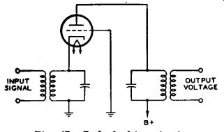
Fig. 47-Cathode-drive circuit.
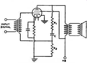
Fig. 48-Power-output stage using constant voltage inverse feedback.
Inverse Feedback
An inverse-feedback circuit, some times called a degenerative circuit, is one in which a portion of the output voltage of a tube is applied to the input of the same or a preceding tube in opposite phase to the signal applied to the tube. Two important advantages of feedback are (1) reduced distortion from each stage included in the feedback circuit and (2) reduction in the variations in gain due to changes in line voltage, possible differences between tubes of the same type, or variations in the values of circuit constants included in the feed back circuit.
Inverse feedback is used in audio amplifiers to reduce distortion in the output stage where the load impedance on the tube is a loudspeaker. Because the impedance of a loudspeaker is not constant for all audio frequencies, the load impedance on the output tube varies with frequency. When the output tube is a pentode or beam power tube having high plate resistance, this variation in plate load impedance can, if not corrected, produce considerable frequency distortion. Such frequency distortion can be reduced by means of inverse feedback. Inverse-feedback circuits are of the constant-voltage type and the constant-current type.
The application of the constant voltage type of inverse feedback to a power-output stage using a single beam power tube is illustrated in Fig. 48. In this circuit, R1, R2, and C are connected as a voltage divider across the output of the tube. The secondary winding of the grid-input transformer is returned to a point on this voltage divider. Capacitor C blocks the dc plate voltage from the grid. However, a portion of the tube AF output voltage, approximately equal to the output voltage multiplied by the fraction R./(R1 + R2), is applied to the grid. This voltage reduces the source impedance of the circuit and a decrease in distortion results which is explained in the curves of Fig. 49.
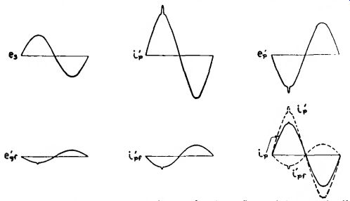
Fig. 49-Voltage and current waveforms showing effect of inverse feedback.
Consider first the amplifier without the use of inverse feedback. Suppose that when a signal voltage e, is applied to the grid the AF plate current i'p has an irregularity in its positive half-cycle.
This irregularity represents a departure from the waveform of the input signal and is, therefore, distortion. For this plate-current waveform, the AF plate voltage has a waveform shown by e',..
The plate-voltage waveform is inverted compared to the plate-current wave form because a plate-current increase produces an increase in the drop across the plate load. The voltage at the plate is the difference between the drop across the load and the supply voltage; thus, when plate current goes up, plate voltage goes down; when plate current goes down, plate voltage goes up.
Now suppose that inverse feedback is applied to the amplifier. The voltage fed back to the grid has the same wave form and phase as the plate voltage, but is smaller in magnitude. Hence, with a plate voltage of waveform shown by e'p , the feedback voltage appearing on the grid is as shown by e' S f. This voltage applied to the grid produces a component of plate current i'„r. It is evident that the irregularity of the waveform, of this component of plate current would act to cancel the original irregularity and thus reduce distortion.
After inverse feedback has been applied, the relations are as shown in the curve for i P . The dotted curve shown by i'pf is the component of plate current due to the feedback voltage on the grid.
The dotted curve shown by i'p is the component of plate current due to the signal voltage on the grid. The algebraic sum of these two components gives the resultant plate current shown by the solid curve of ip . Since i'P is the plate current that would flow without inverse feedback, it can be seen that the application of inverse feedback has reduced the irregularity in the output current.
In this manner inverse feedback acts to correct any component of plate current that does not correspond to the input signal voltage, and thus reduces distortion.
From the curve for ip , it can be seen that, besides reducing distortion, inverse feedback also reduces the amplitude of the output current. Consequently, when inverse feedback is applied to an amplifier there is a decrease in gain or power sensitivity as well as a decrease in distortion. Hence, the application of inverse feedback to an amplifier requires that more driving voltage be applied to obtain full power output, but this output is obtained with less distortion.
Inverse feedback may also be applied to resistance-coupled stages, as shown in Fig. 50. The circuit is conventional except that a feedback resistor, B-C+ ...
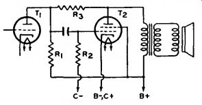
Fig. 50-Resistance-coupled stages using feedback resistor.
... R3 , is connected between the plates of tubes T1 and T2. The output signal voltage of T1 and a portion of the output signal voltage of T2 appear across R2.
Because the distortion generated in the plate circuit of Ts is applied to its grid out of phase with the input signal, the distortion in the output of T2 is comparatively low. With sufficient inverse feedback of the constant-voltage type in a power-output stage, it is not necessary to employ a network of resistance and capacitance in the output circuit to reduce response at high audio frequencies. Inverse-feedback circuits cap also be applied to push-pull class A and class AB1 amplifiers.
Constant-current inverse feedback is usually obtained by omitting the by pass capacitor across a cathode resistor.
This method decreases the gain and the distortion but increases the source impedance of the circuit. Consequently, the output voltage rises at the resonant frequency of the loudspeaker and accentuates hangover effects.
Inverse feedback is not generally applied to a triode power amplifier be cause the variation in speaker impedance with frequency does not produce much distortion in a triode stage having low plate resistance. It is sometimes applied in a pentode stage, but is not always convenient. As has been shown, when inverse feedback is used in an amplifier, the driving voltage must be increased in order to provide full power output. When inverse feedback is used with a pentode, the total driving voltage required for full power output may be inconveniently large, although still less than that required for a triode. Because a beam power tube gives full power output on a comparatively small driving voltage, inverse feedback is especially applicable to beam power tubes. By means of inverse feedback, the high efficiency and high power output of beam power tubes can be combined with freedom from the effects of varying speaker impedance.
Cathode-Follower Circuits
Another important application of inverse feedback is in the cathode-follower circuit, an example of which is shown in Fig. 5 1. In this application, the load has been transferred from the plate circuit to the cathode circuit of the tube.
The input voltage is applied between the grid and ground, and the output voltage is obtained between the cathode and ground. The voltage amplification (V.A.) of this circuit is always less than unity and may be expressed by the following convenient formulas.
For a triode:
For a pentode:
In these formulas, fi is the amplification factor, R1 is the load resistance in ohms, r„ is the plate resistance in ohms, and g,„ is the transconductance in mhos.
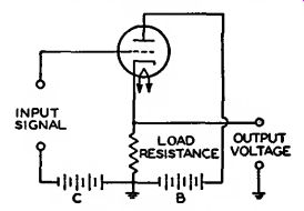
Fig. 51-Cathode-follower circuit.
The use of the cathode follower permits the design of circuits which have high input resistance and high output voltage. The output impedance is quite low and very low distortion may be obtained. Cathode-follower circuits may be used for power amplifiers or as impedance transformers designed either to match a transmission line or to produce a relatively high output voltage at a low impedance level.
In a power amplifier which is transformer coupled to the load, the same output power can be obtained from the tube as would be obtained in a conventional grid-drive type of amplifier. The output impedance is very low and provides excellent damping to the load, with the result that very low distortion can be obtained. The peak-to-peak signal voltage, however, approaches Wi times the plate supply voltage if maximum power output is required from the tube. Some problems may be encountered, therefore, in the design of an adequate driver stage for a cathode follower output system.
When a cathode-follower circuit is used as an impedance transformer, the load is usually a simple resistance in the cathode circuit of the tube. With relatively low values of cathode resistor, the circuit may be designed to supply significant amounts of power and to match the impedance of the device to a transmission line. With somewhat higher values of cathode resistor, the circuit may be used to decrease the output impedance sufficiently to permit the transmission of audio signals along a line in which appreciable capacitance is present.
The cathode follower may also be used as an isolation device to provide extremely high input resistance and low input capacitance as might be required in the probe of an oscilloscope or vacuum-tube voltmeter. Such circuits can be designed to provide effective impedance transformation with no significant loss of voltage.
Selection of a suitable tube and its operating conditions for use in a cathode-follower circuit having a specified output impedance (Z„) can be made, in most practical cases, by the use of the following formula to determine the approximate value of the required tube transconductance.
Required gm (/tmhos) :
1.000,000 Zo (ohms) from the technical data given in the Technical Data section. The tube selected should have a value of transconductance slightly lower than that obtained from the above expression to allow for the shunting effect of the cathode load resistance. The conversion nomograph given in Fig. 44 may be used for calculation of operating conditions for values of transconductance not included in the tabulated data. After the operating conditions have been determined, the approximate value of the required cathode load resistance may be calculated from the following formulas.
For a triode:
Zo X rP rp - [Zo X (1 + A)l
Cathode Rr. =
For a pentode:
Cathode Rr. = , ^ - 1 - (gm X Zo)
Resistance and impedance values are in ohms; transconductance values are in mhos.
If the value of the cathode load resistance calculated to provide the required output impedance does not provide the required operating bias, the basic cathode-follower circuit can be modified in a number of ways. Two of the more common modifications are shown in Figs. 52 and 53.
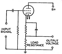
Fig. 52--Cathode-follower circuit modified for increased bias.
In Fig. 52 the bias is increased by adding a bypassed resistance between Once the required transconductance is obtained, a suitable tube and its operating conditions may be determined the cathode and the unbypassed load resistance and returning the grid to the low end of the load resistance. In Fig. 53 the bias is reduced by adding a by passed resistance between the cathode and the unbypassed load resistance but, in this case, the grid is returned to the junction of the two cathode resistors so that the bias voltage is only the dc voltage drop across the added resistance The size of the bypass capacitor should be large enough so that it has negligible reactance at the lowest frequency to be handled. In both cases the B-supply should be increased to make up for the voltage taken for biasing.
LOAD OUTPUT RESISTANCE VOLTAGE
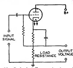
Fig. 53--Cathode-follower circuit modified for reduced bias.
Example: Select a suitable tube and determine the operating conditions and circuit components for a cathode follower circuit having an output impedance that will match a 500-ohm transmission line.
Procedure: First, determine the approximate transconductance required.
1 .000,000 500
Required gm = : 2000 /imhos
A survey of the tubes that have a transconductance in this order of magnitude shows that type 12AX7A is among the tubes to be considered. Referring to the characteristics given in the technical data section for one triode unit of high mu twin triode 12AX7, we find that for a plate voltage of 250 volts and a bias of -2 volts, the transconductance is 1600 micromhos, the plate resistance is 62500 ohms, the amplification factor is 100, and the plate current is 0.0012 ampere. When these values are used in the expression for determining the cathode load resistance, the following result is obtained:
Cathode Ri.=
500 X 62500
=2600 ohms "62500-500XOOO+ 1)"
The voltage across this resistor for a plate current of 0.0012 ampere is 2600 x 0.0012 = 3.12 volts. Because the required bias voltage is only - volts, the circuit arrangement given in Fig. 53 is employed. The bias is furnished by a resistance that will have a voltage drop of 2 volts when it carries a current of 0.0012 ampere. The required bias resistance, therefore, is 2/0.0012 = 1670 ohms. If 60 Hz is the lowest frequency to be passed, 20 microfarads is a suitable value for the bypass capacitor. The B-supply, of course, is increased by the voltage drop across the cathode resistance which, in this example, is approximately 5 volts.
The B-supply, therefore, is 250 + 5 = 255 volts.
Because it is desirable to eliminate, if possible, the bias resistor and bypass capacitor, it is worthwhile to try other tubes and other operating conditions to obtain a value of cathode load resistance which will also provide the required bias. If the triode section of twin diode-high-mu triode 6AT6 is operated under the conditions given in the technical data section with a plate voltage of 100 volts and a bias of -1 volt, it will have an amplification factor of 70, a plate resistance of 54000 ohms, a transconductance of 1300 micromhos, and a plate current of 0.0008 ampere.
Then, Cathode R1 =500 X 54000
54000 - 500 X (70 + 1) = 1460 ohms
The bias voltage obtained across this resistance is 1460 X 0.0008 = 1.17 volts. Since this value is for all practical purposes close enough to the required bias, no addition bias resistance will be required and the grid may be returned directly to ground. There is no need to adjust the B-supply voltage to make up for the drop in the cathode resistor. The voltage amplification (V.A.) for the cathode-follower circuit utilizing the triode section of type 6AT6 is 70 X 1460 V.A. = 0.65 54000 + 1460 X (70 + 1 For applications in which the cathode follower is used to isolate two circuits--for example, when it is used between a circuit being tested and the input, stage of an oscilloscope or a vacuum-tube voltmeter-voltage output and not impedance matching is the primary consideration. In such applications it is desirable to use a relatively high value of cathode load resistance, such as 50,000 ohms, in order to get the maximum voltage output. In order to obtain proper bias, a circuit such as that of Fig. 53 should be used. With a high value of cathode resistance, the voltage amplification will approximate unity.
Corrective Filters
A corrective filter can be used to improve the frequency characteristic of an output stage using a beam power tube or a pentode when inverse feed back is not applicable. The filter consists of a resistor and a capacitor connected in series across the primary of the output transformer. Connected in this way, the filter is in parallel with the plate load impedance reflected from the voice coil by the output transformer. The magnitude of this reflected impedance increases with increasing frequency in the middle and upper audio range. The impedance of the filter, however, decreases with increasing frequency. It follows that, by use of the proper values for the resistance and the capacitance in the filter, the effective load impedance on the output tubes can be made practically constant for all frequencies in the middle and upper audio range. The result is an improvement in the frequency characteristic of the output stage.
The resistance to be used in the filter for a push-pull stage is 1.3 times the recommended plate-to-plate load resistance; or, for a single-tube stage, is 1.3 times the recommended plate load resistance. The capacitance in the filter should have a value such that the voltage gain of the output stage at a frequency of 1000 Hz or higher is equal to the voltage gain at 400 Hz.
A method of determining the proper value of capacitance for the filter is to make two measurements of the output voltage across the primary of the output transformer: first, when a 400-Hz signal is applied to the input, and second, when a 1000-Hz signal of the same voltage as the 400-Hz signal is applied to the input. The correct value of capacitance is the one which gives equal output voltages for the two signal inputs. In practice, this value is usually found to be in the order of 0.05 microfarad.

Fig. 54--Simple RC frequency-compensation network.
The dynamic range of an amplifier is a measure of its signal-handling capability. The dynamic range expresses in dB the ratio of the maximum usable output signal (generally for a distortion of about 10 percent) to the minimum usable output signal (generally for a signal-to-noise ratio of about 20 dB). A dynamic range of 40 dB is usually acceptable; a value of 70 dB is exceptional for any audio system.
Phonograph and Tape Preamplifiers
The frequency range and dynamic range which can be recorded on a phonograph record or on magnetic tape depend on several factors, including the composition, mechanical characteristics, and speed of the record or tape, and the electrical and mechanical characteristics of the recording equipment. To achieve wide frequency and dynamic ranges, manufacturers of commercial recordings use equipment which introduces a nonuniform relationship between amplitude and frequency. This relationship is known as a "recording characteristic." To assure proper reproduction of a high-fidelity recording, therefore, some part of the reproducing system must have a frequency-response characteristic which is the inverse of the recording characteristic. Most manufacturers of high-fidelity recordings use the RIAA characteristic for discs and the NARTB characteristic for magnetic tape.
The simplest type of equalization network is shown in Fig. 54. Because the capacitor C is effectively an open circuit at low frequencies, the low frequencies must be passed through the resistor R and are attenuated. The capacitor has a lower reactance at high frequencies, however, and bypasses high-frequency components around R so that they receive negligible attenuation.
Thus the network effectively "boosts" the high frequencies. This type of equalization is called "attenuative." Some typical preamplifier stages are shown in the Circuits section. The location of the frequency-compensating network or "equalizer" in the reproducing system will depend on the types of recordings which are to be reproduced and on the pickup devices used.
A ceramic high-fidelity phonograph pickup is usually designed to provide proper compensation for the RIAA recording characteristic when the pickup is operated into the load resistance specified by its manufacturer. Because this type of pickup also has relatively high output (0.5 to 1.5 volts), it does not require the use of either an equalizer network or a preamplifier, and can be connected directly to the input of a tone-control amplifier and/or power amplifier.
A magnetic high-fidelity phono graph pickup, on the other hand, usually has an essentially flat frequency-response characteristic and very low output (1 to 10 millivolts). Because a pickup of this type merely reproduces the recording characteristic, it must be followed by an equalizer network, as well as by a preamplifier having sufficient voltage gain to provide the input voltage required by the tone-control amplifier and /or power amplifier. Many designs include both the equalizing and amplifying circuits in a single unit.
A high-fidelity magnetic-tape pick up head, like a magnetic phonograph pickup, reproduces the recording characteristic and has an output of only a few millivolts. This type of pickup device, therefore, must also be followed by an equalizing network and preamplifier, or by a preamplifier which provides "built-in" equalization for the NARTB characteristic.
Feedback networks may also be used for frequency compensation and for reduction of distortion. Basically, a feedback network returns a portion of the output signal to the input circuit of an amplifier. The feedback signal may be returned in phase with the input signal (positive or regenerative feed back) or 180 degrees out of phase with the input signal (negative, inverse, or degenerative feedback). In either case, the feedback can be made proportional to either the output voltage or the output current, and can be applied to either the input voltage or the input current.
A negative feedback signal proportional to the output current raises the output impedance of the amplifier; negative feedback proportional to the output voltage reduces the output impedance.
A negative feedback signal applied to the input current decreases the input impedance; negative feedback applied to the input voltage increases the input impedance. Opposite effects are produced by positive feedback.

Fig. 55-Negative-feedback frequency-compensation network.
A simple negative or inverse feed frequency boost is shown in Fig. 55.
back network which provides high This network provides equalization comparable to that obtained with Fig. 54, but is more suitable for low-level amplifier stages because it does not require the first amplifier stage to provide high-level low frequencies. In addition, the inverse feedback improves the distortion characteristics of the amplifier.
Some preamplifier or low-level audio amplifier circuits include variable resistors or potentiometers which function as volume or tone controls. Such circuits should be designed to minimize the flow of dc currents through these controls so that little or no noise will be developed by the movable contact during the life of the circuit. Volume controls and their associated circuits should permit variation of gain from zero to maximum, and should attenuate all frequencies equally for all positions of the variable arm of the control. Several examples of volume controls and tone controls are shown in the Circuits section.
Tone Controls
A tone control is a variable filter (or one in which at least one element is adjustable) by means of which the user may vary the frequency response of an amplifier to suit his own taste. In radio receivers and home amplifiers, the tone control usually consists of a resistance capacitance network in which the resistance is the variable element.
The simplest form of tone control is a fixed tone-compensating or "equalizing" network such as that shown in Fig. 56. This type of network is often used to equalize the low- and high-frequency response of a crystal phono graph pickup. At low frequencies the attenuation of this network is 20.8 dB.
As the frequency is increased, the 100-picofarad capacitor serves as a bypass for the 5-megohm resistor, and the combined impedance of the resistor capacitor network is reduced. Thus, more of the crystal output appears across the 0.5-megohm resistor at high frequencies than at low frequencies, and the frequency response at the grid is reasonably flat over a wide frequency range. Fig. 57 shows a comparison between the output of the crystal (curve A) and the output of the equalizing network (curve B). The response curve can be "flattened" still more if the attenuation at low frequencies is increased by changing the 0.5-megohm resistor to 0.125 megohm.
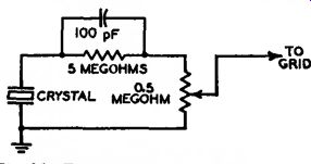
Fig. 56-Tone-control circuit for fixed tone compensation or "equalizing".
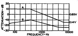
Fig. 57-Curve showing output from crystal phonograph pickup (A) and
from equalizing network (B).
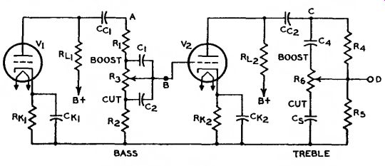
Fig. 58-Two-stage tone-control circuit incorporating separate bass and
treble controls.
The tone-control network shown in Fig. 58 has two stages with completely separate bass and treble controls. Fig. 59 shows simplified representations of the bass control of this circuit when the potentiometer is turned to its extreme variations (usually labeled "Boost" and "Cut"). In this network, as in the crystal-equalizing network shown in Fig. 56, the parallel RC combination is the controlling factor. For bass "boost," the capacitor Cs bypasses resistor R« so that less impedance is placed across the output to grid B at high frequencies than at low frequencies. For bass "cut," the parallel combination is shifted so that C1 bypasses Ra, causing more high frequency than low-frequency output Essentially, the network is a variable- frequency voltage divider. With proper values for the components, it may be made to respond to changes in the R > potentiometer setting for only low frequencies (below 1000 Hz).
BASS BOOST
A R| I %1 B CWW^-*-vW O R3 J R2
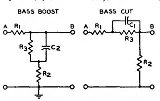
Fig. 59--Simplified representations of bass control circuit at extreme
ends of potentiometer.
Fig. 60 shows extreme positions of the treble control. The attenuation of the two circuits is approximately the same at 1000 Hz. The treble "boost" circuit is similar to the crystal-equalizing network shown in Fig. 56. In the treble "cut" circuit, the parallel RC elements serve to attenuate the signal voltage further because the capacitor by passes the resistance across the output.
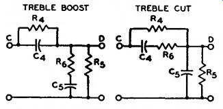
Fig. 60--Simplified representations of treble-control circuit at extreme
ends of potentiometer.
The effect of the capacitor is negligible at low frequencies; beyond 1000 Hz, the signal voltage is attenuated at a maximum rate of 6 dB per octave.
The location of a tone-control net work is of considerable importance. In a typical radio receiver, it may be inserted in the plate circuit of the power tube, the coupling circuit between the first AF amplifier tube and the power tube, or the grid circuit of the first tube. In an amplifier using a beam power tube or pentode power amplifier without negative feedback, it is desirable to connect a resistance capacitance filter across the primary of the output transformer. This filter may be fixed, with a supplementary tone control elsewhere, or it may form the tone control itself. If the amplifier incorporates negative feedback, the tone control may be inserted in the feedback network or else should be connected to a part of the amplifier which is external to the feedback loop. The over all gain of a well designed tone-control network should be approximately unity.