Introduction
WE have so far discussed the use of transistors as amplifiers and we shall now consider transistor oscillators, detectors and frequency changers. We shall then have described all the operations necessary in a receiver and can consider the design of complete transistor superheterodyne receivers.
OSCILLATORS
Oscillators have two main sections: a frequency-determining section and a maintaining section. The frequency-determining section commonly consists of an LC circuit or RC network. The maintaining section is commonly a valve or transistor amplifier which must have sufficient gain to make up for losses in the frequency-determining section to give rise to the positive feedback which causes oscillation.
In one type of oscillator the amplifier is used purely as a switch, the valves or transistors being in a state of conduction or of non conduction (i.e. cut off) for most of the period of oscillation. The changes of state are very rapid and the shape of the input-output characteristic of the amplifier (which is of great importance in class-A amplification) is unimportant in this application. Such oscillators are termed relaxation oscillators and their period of oscillation is usually determined by the time constants of RC or RL networks.
The output waveform of such oscillators is largely made up of linear and exponential sections. Typical of such oscillators are multivibrators and blocking oscillators.
In a second type of oscillator, the maintaining section is used as a linear amplifier and is in operation for the whole or a substantial fraction of each cycle of oscillation. The output waveform is sinusoidal and the frequency-determining system is commonly, though not invariably, an LC circuit. Hartley and Colpitts oscillators are of this type.
In general, transistor oscillators are of the same basic types as thermionic-valve oscillators and their circuits can be deduced by analogy with the valve circuits. It may, however, be necessary to modify the circuit to suit the input and output resistances of the transistors where these differ markedly from those of a valve.
In this chapter we are primarily concerned with the application of junction transistors in sinusoidal oscillators, particularly those
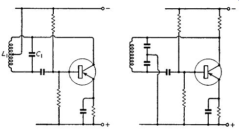
Fig. 11.1. One possible circuit for a transistor Hartley oscillator
Fig. 11.2. One possible circuit for a transistor Colpitts oscillator used in receivers. Some information about the use of junction transistors in relaxation oscillators is given in Chapter 12.
When a signal is momentarily induced in an LC circuit, it gives rise to an oscillation which is at the resonance frequency of the circuit and dies away exponentially due to dissipation in the resistance of the circuit. To maintain the oscillation at constant amplitude the loss of power must be made good: this may be achieved by connecting the LC circuit to a source of power such as an amplifier. This source can be regarded as having a negative input resistance which neutralizes the positive resistance of the tuned circuit. In the Hartley, Colpitts and Reinartz circuits the negative input resistance is achieved by positive feedback, i.e., by establishing a connection between the input and output circuits of the maintaining amplifier. It is characteristic of these forms of oscillator that at least three connections must be made to the LC circuit to obtain the required positive feedback.
Fig. 11.1 gives the circuit diagram of a Hartley transistor oscillator.
The steady component of the transistor collector current is stabilized by the potential divider method and, except for the components associated with the stabilization, the circuit is similar to that of a ...
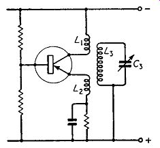
Fig. 11.3. One possible circuit for a transistor Reinartz oscillator
... thermionic-valve Hartley oscillator. The frequency-determining section L1C1 is connected between collector (anode) and base (grid). The emitter (cathode) is effectively connected to the centre tap of the inductor because both these points are at zero r.f. potential. The circuit illustrated is a series-fed type in which the collector current flows through part of the inductor. There is an alternative shunt-fed circuit in which the transistor has a resistive collector load and the collector is connected to the top end of the inductor by a fixed capacitor.
Fig. 11.2 gives the circuit diagram for a Colpitts oscillator, also d.c.-stabilized by the potential-divider method.
The circuit diagram for a Reinartz-type transistor oscillator is given in Fig. 11.3: this circuit is of interest because it is frequently used in transistor receivers. Regeneration in this circuit is obtained by coupling the collector circuit to the emitter circuit via the mutual inductance between L1 and L2. Both inductors are also coupled to the frequency-determining circuit L3C3. This circuit is also d.c.-stabilized by the potential-divider method. It could, of course, be simplified by omitting the components L3 and C3 and connecting a tuning capacitance across L1 or L2, but the form illustrated here enables the moving vanes of the tuning capacitor to be earthed. Moreover, this helps frequency stability by isolating L3C3 to some extent from variations in transistor parameters.
A.M. DETECTORS
The purpose of the detector in a receiver is to derive from a modulated carrier a substantially-undistorted copy of the modulation waveform. Frequently an a.m. detector also has to produce an output signal, proportional to the carrier amplitude, which can be used for automatic gain control and in a transistor receiver appreciable power is necessary for a.g.c. Point-contact diodes are often used for detection in transistor receivers: they are satisfactory in providing the a.f. output and the provision of a.g.c. is not difficult.
Transistors can be used for a.m. detection also and they have the advantage over point-contact diodes that they give substantial gain ( e.g. 20 dB) and can readily supply the power necessary for a.g.c, The circuit of a common-emitter transistor a.m. detector is given in Fig. 11.4. The potential divider method of d.c. stabilization is again used and the value of Re must be chosen to give the required value of collector and emitter current. The value of the emitter current
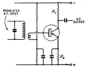
Fig. 11.4. One circuit for a common-emitter transistor a.m. detector is
particularly important in an a.m. detector and its value must be a compromise
between the following two conflicting requirements:
(1) The emitter-base junction must be biased to a point on the dynamic characteristic where the curve has a sharp knee.
It is essential to use an r.f. type of transistor because the input is r.f. and the emitter current is usually low when optimum bias is applied.
(2) The transistor also operates as an a.f. amplifier and for maximum gain from such an amplifier the collector current (and hence the emitter current) must be of the order of 1 mA. Low emitter currents give good demodulation but poor a.f. gain; high emitter currents good a.f. gain but poor demodulation. It is not surprising, therefore, that there is an optimum value of emitter current which gives maximum a.f. output for a given modulated r.f. input, and for germanium transistors this is commonly of the order of 50 µA. A suitable value for the collector load resistance is 15 k-ohm and the voltage drop across this for a collector current of:
50 µA is 50 x 10^-6 x 15 x 10^3
= 750 x 10^-3
= 0.75 volt
This is the voltage across Re when there is no input signal. When an input signal is applied the mean collector current rises causing an increased voltage drop across Re. The collector potential thus becomes less negative, i.e., more positive, the polarity required in one type of a.g.c. circuit. Such a.g.c. is more effective than that obtainable from a simple diode detector because of the amplification available.
The input resistance of a common-emitter amplifier is commonly quoted as approximately 1 k-ohm. This applies when the emitter current is approximately 1 mA. In the common-emitter detector, however, the emitter current is much smaller than this and the input resistance is therefore much higher, commonly greater than 10 k-ohm. The damping imposed by the detector on the tuned circuit feeding it is thus not as heavy as might be feared. Nevertheless it is usually necessary to feed the detector from a tapping point on the inductor or, as shown in Fig. 11.4, from a small coil closely coupled to the tuning inductor to avoid too great a reduction in the Q. value.
AUTOMATIC GAIN CONTROL
A.g.c. is used in radio receivers for two main reasons:
(1) It combats fading. Fading is experienced quite generally in radio reception but it is particularly troublesome during medium-wave reception after nightfall.
(2) It helps to prevent overloading of later stages. In transistor receivers without a.g.c. overloading of the final i.f. stage would occur on strong signals.
A.g.c. is achieved by feeding back to pre-detector stages (usually i.f. stages) a control voltage proportional to the carrier amplitude at the detector. This control voltage has the effect of reducing the gain of the controlled stages. Strong signals give a large control voltage and low i.f. gain; weak signals give a small control voltage and high i.f. gain.
The control voltage must reduce the gain of the i.f. stages and there are two methods by which the gain of a transistor amplifier can be controlled:
(1) By reducing the emitter current, keeping the collector voltage constant. For germanium transistors the gain tends to be proportional to the square root of the emitter current, provided this is below approximately 500 µA.
(2) By reducing the collector voltage, keeping the emitter current constant. For germanium transistors the gain tends to be proportional to the square root of the collector voltage, provided this is below approximately 500 m V. Both methods of gain control reduce the signal-handling capacity of the amplifier and to avoid distortion due to peak clipping the controlled stages must at all times have small input signals. It is not advisable therefore to control the final i.f. amplifier, for this has to deliver a reasonably large signal to the detector, particularly if this is a diode which has to supply the control voltage. The reduction of signal-handling capacity of the controlled transistors contrasts with the behavior of automatic-gain-controlled valves: the application of negative bias to the control grid of a variable-mu pentode lengthens the grid base and improves signal-handling capacity.
Gain control by adjustment of emitter current is rarely achieved directly, i.e., by control of the emitter voltage of a common-base amplifier. This is because the input resistance of the emitter circuit is so low (50 ohms is typical) that considerable power input is necessary to produce appreciable change in current and thus in gain.
It is usual to control the emitter current indirectly, e.g., by control of the base potential in a common-emitter amplifier. In this way the current gain of the transistor is utilized for a.g.c. purposes. Moreover the input resistance of a common-emitter amplifier is higher (1 k-O is typical) than for a common-base amplifier.
A typical circuit diagram for an amplifier with base injection of a.g.c. voltage is given in Fig. 11.5. The voltage must be positive going in order to reduce emitter current in a pnp transistor and ...
R.F. OR I.F. AMPLIFIER DETECTOR
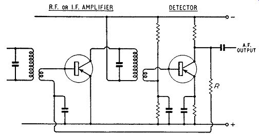
Fig. 11.5. An a.g.c. circuit using emitter-current control
... such a polarity can be obtained from a common-emitter detector as shown in this diagram. The resistance R should be so adjusted that, in the absence of an input signal, the controlled stage has a collector current of approximately 500 µA. A larger collector current gives an effective delay to the a.g.c. because little reduction in gain occurs until the collector current has fallen below approximately 500 µA. For the sake of simplicity, neutralizing is omitted from the diagram and no means is indicated of preventing thermal runaway of the r.f. or i.f. amplifier.
A.g.c. by control of collector voltage is also achieved indirectly and a typical circuit is given in Fig. 11.6. This shows a common emitter stage with the control voltage applied to the base. The collector circuit decoupling resistor R1 is an essential feature of this circuit. The control voltage must be negative-going in this circuit to increase the collector current on strong signals. The value of the decoupling resistor is so chosen that the collector-emitter voltage is approximately 500 m V in the absence of a signal. Any increase in base current due to a.g.c. action increases emitter current and hence collector current, decreasing collector voltage and gain. A typical value for the decoupling resistance is 15 k-O. The required polarity of a.g.c. voltage is obtained in this circuit by taking the control voltage from the emitter of a common-emitter detector.
The circuit is again simplified by the omission of neutralizing and the means of preventing thermal runaway.
Attention must be paid in the design of a.g.c. circuits to the effects on receiver performance of the inevitable variations in transistor input and output impedances brought about by the changes in d.c. conditions. The input and output impedances of a transistor both have resistive and reactive components. The resistive component causes damping of the input and output tuned circuits and the capacitive component causes mistuning of these circuits. The severity of the damping and the extent of the mistuning both depend on the emitter current and both therefore change with alterations in a.g.c. voltage. The mistuning effect can be minimized by so designing the circuit that the variations ...
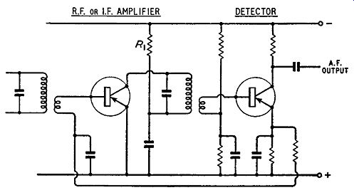
Fig. 11.6. An a.g.c. circuit using collector-voltage control
... in transistor capacitance are small compared with that already present in the input and output tuned circuits. The variations in damping are, however, more difficult to minimize, and some decrease in damping is probably inevitable as emitter current is reduced.
However, the variations in damping need not always be undesirable. For example, in an a.g.c. circuit using collector-voltage control the emitter current increases when a strong signal is received.
This causes increased damping and hence a wider i.f. passband.
This is an advantage in receiving a strong local signal because it permits better quality of reproduction on a signal which is large enough to swamp any interference. When the receiver is tuned to a weak signal, the damping is reduced and the passband narrowed.
In the alternative a.g.c. circuit using emitter-current control the emitter current is reduced when a strong signal is tuned in, giving minimum passband on stronger signals. However, this method gives less mistuning than the other and, in general, emitter-current control is preferred.
F.M. DETECTORS
The function of an f.m. detector is to derive from a frequency modulated signal a substantially-undistorted copy of the modulated waveform impressed on the signal. There are many types of f.m. detector but only two are in common use in f.m. receivers: these are the Foster-Seeley discriminator and the ratio detector. The method of operation of these detectors is complex and only a brief summary of it is given below: for a more complete description the reader is referred to other books*.
Foster-Seeley Discriminator
This discriminator contains two diode detectors so arranged that their outputs are connected in series opposition. The diodes are fed from a double-tuned transformer, the primary and secondary windings of which are resonant at the centre frequency of the pass band to be covered. An essential feature of the circuit is that a fraction of the primary voltage is fed to the centre point of the secondary winding. In Fig. 11. 7 this is achieved by a connection between the centre point of L2 and a tapping point on L1 but the secondary connection could be to the junction of two equal capacitors across L2 (they could together constitute the tuning capacitance) and the primary connection could be to an inductor closely coupled to L1 or to a capacitive potential divider across L1 (formed by two capacitors which may also provide the tuning capacitance).
[*For example, B. S. Carnies" Principles of Frequency Modulation" I, Books Ltd.]
For signals at the centre frequency, diodes D1 and D2 receive equal inputs and the voltages generated across R1 and R2 are equal, giving zero resultant voltage across (R1 + R2). The effect of the interconnection between primary and secondary windings is that for signals displaced from the centre value one diode receives a bigger input than the other. The voltages across R1 and R2 are then no longer equal and there is a net output across (R1 + R2), ...
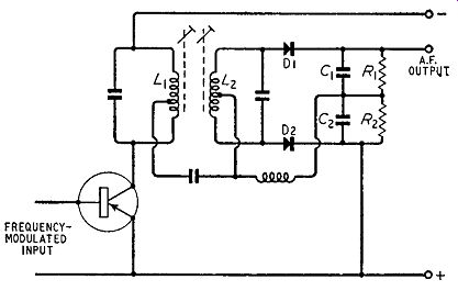
Fig. 11.7. One circuit for a Foster-Seeley discriminator
... the polarity depending on the direction of the frequency displacement and the magnitude depending on the extent of the displacement. If, therefore, a frequency-modulated signal is applied to the discriminator, a copy of the modulation waveform is generated across (R1 + R2).
The Foster-Seeley discriminator gives zero output at the centre frequency and at this frequency the output is independent of the magnitude of the signal input to the detector. At other frequencies the output of the discriminator is proportional both to frequency displacement and to signal input. Ideally the output of an f.m. detector should be proportional to the frequency displacement but independent of the signal input. If this can be achieved the full advantages of frequency modulation are realised and the receiver is to a large extent immune from interference due to a.m. signals and from the distortion due to multi-path reception. The Foster Seeley discriminator thus has poor ability to reject a.m. signals and is normally used with a separate limiter stage in order to obtain a satisfactory performance.
Ratio Detector
The ratio detector has much better a.m. rejection than a Foster Seeley circuit and nearly all commercial receivers employ a ratio detector.
The circuit diagram of one form of ratio detector is given in Fig. 11.8. It has two diodes and a double-tuned transformer with a primary-secondary connection similar to that employed ...
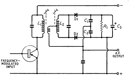
Fig. 11.8. One circuit for a ratio detector.
... in the Foster-Seeley circuit but the diodes are connected in a series-aiding arrangement and supply a common load resistor.
This resistor has a low value to give the heavy damping of the secondary tuned circuit on which the limiting properties of the detector depend. The load resistor is bypassed by a high-value capacitor giving a load time constant of 0.1 second. The diodes conduct continuously when a signal is applied to the detector and give a voltage across the load circuit proportional to the carrier input: the maximum value of this voltage gives an indication of the correct tuning point. The inputs to the two diodes vary with frequency displacement (as in the Foster-Seeley circuit) and the voltages generated across the reservoir capacitors C1 and C2 vary also although the total voltage across (C1 + C2) is independent of input frequency, being stabilized at a value proportional to carrier input amplitude by the long time constant R1C3. One end of the capacitor C3 is earthed usually and the a.f. output is taken from the junction of C1 and C2. Practical ratio detector circuits commonly employ additional resistors in series with the diodes: by choosing suitable values for these resistors, the a.m. rejection of the detector can be significantly improved.
MIXERS In a superheterodyne receiver the carrier and sidebands constituting the received signal are in effect translated in frequency to give a new signal with a carrier at the intermediate frequency. This is achieved in a mixer stage in which the received signal is combined with the output of a local oscillator, thereby producing a resultant signal at the sum or difference of the received carrier and oscillator frequencies.
In general, there are two basic principles which can be applied to produce an output with a frequency equal to the difference between the frequencies of two input signals. In one method the two input signals are simply connected in series or in parallel and applied between two electrodes such as the grid and cathode of a valve or the base and emitter of a transistor. If the input-output relationship for the valve or transistor is linear, these two signals are amplified independently and there is no output at any frequency other than frequencies of the two input signals. To produce interaction between the two original signals, thus obtaining an output at the difference frequency, it is essential that the valve or transistor should have a non-linear characteristic, i.e., should behave as a detector.
For this reason the mixers of early superheterodyne receivers were known as first detectors. Stages of this type are known as additive mixers and they are usually biased near the point of anode or collector-current cut off to achieve the non-linearity essential for their action.
In another, more modern, type of mixer the received signal and the local oscillator output are in effect multiplied together. This is achieved by applying the two inputs to separate electrodes of a valve or transistor which is so designed that a signal applied to one electrode controls the gain of a signal applied to the other electrode. Two such electrodes are the control grid and suppressor grid of a pentode. In a mixer of this type there is no need for any non-linearity, the output at the difference frequency being produced directly from the effective multiplication of the two input signals. Such mixers are termed multiplicative, and most modern mixers are of this type. Clearly it is wrong therefore to refer to such mixers as first detectors because they can be linear devices.
A multiplicative type of mixer requires a valve or transistor with two input electrodes, and mixer valves commonly have a total of at least six electrodes. It is possible that transistors of an analogous type may in time be developed, but at the moment most transistors are triodes with which it is difficult if not impossible to construct a multiplicative type of mixer; transistor mixers must
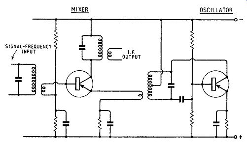
Fig. 11.9. One possible circuit for a two-transistor frequency changer operate
therefore on the additive principle and this can be achieved by applying
both input signals between base and emitter. Most transistor receivers employ
an additive mixer of this type and one possible circuit is given in Fig.
11.9. This also gives the circuit of the oscillator stage; the combination
of the two constitutes a frequency-changer stage.
In this circuit the mixer operates in the common-emitter mode and the two input signals are connected in series and applied to the base-emitter circuit. The operating point is swept over the characteristic by the local oscillation, and the efficiency of the mixing process depends on the amplitude of oscillation injected into the emitter circuit. For small oscillation amplitudes the conversion
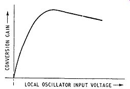
Fig. 11.10. Variation of conversion gain with local-oscillator input voltage
gain, i.e., the ratio of i.f. signal output to r.f. signal input, increases
linearly with oscillation amplitude but levels off at a particular amplitude
and then falls as shown in Fig. 11.10.
Increase in oscillator amplitude beyond this point causes little change in gain.
In a receiver in which the oscillator has to operate over a range of frequency, some variation in oscillator amplitude is inevitable.
In order to prevent such variations causing large changes in conversion gain the oscillator amplitude is usually designed so that it is greater than the minimum critical value which gives maximum gain.
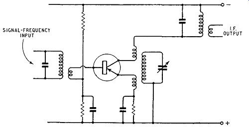
Fig. 11.11. One possible circuit for a self-oscillating mixer
Self-oscillating Mixers It is quite possible to arrange for a single transistor to perform the functions of mixing and of oscillation, and the conversion gain of such a circuit is little short of that available from circuits in which separate transistors are used for the two purposes. One circuit for a self-oscillating mixer is given in Fig. 11.11. This may be regarded as a Reinartz oscillator of the type shown in Fig. 11.3 in which the base circuit is tuned to accept the signal-frequency input and the output circuit is tuned to select the difference frequency output. The oscillator signal and the signal-frequency input are connected in series between base and emitter to enable the transistor to operate as an additive mixer. Circuits of this type are commonly employed in transistor superheterodyne receivers for a.m. reception.
Fig. 11.12 shows a form of self-oscillating mixer suitable for use in v.h.f. receivers: part of the preceding r.f. stage is shown on the left of the diagram. The transistor operating conditions are set

Fig. 11.12. A self-oscillating mixer of the Colpitts' type suitable for
use in v.h.f receivers at a value suitable for a self-oscillating mixer by
the potential divider R5R6 which determines the base potential and by the
resistor R4 which determines the emitter current. The transistor circuit
is based on that of a Colpitts' oscillator, the two fundamental capacitors
C9 and C13 being connected in series between collector and base with the
centre point connected to emitter. C12 is the oscillator tuning capacitor
and C11 a trimmer. C12 is ganged with C5 which tunes the signal-frequency
inductor L3 in the collector circuit of the r.f. amplifier. It is desirable
to earth the moving vanes of C6 and C12 but if this is done the base of the
oscillator is at zero r.f. potential. The emitter cannot also be at zero
r.f. potential (as in many Colpitts' oscillators) because C9 would be short-circuited
and oscillation would be impossible. Some reactance is therefore provided
in the emitter circuit by the inclusion of inductor Ls. The signal-frequency
input to the mixer can now be injected into the emitter circuit via C7 to
enable mixing to take place in the base-emitter diode of the frequency changer.
The inclusion of Ls in the emitter circuit of the frequency changer provides
negative feedback which reduces the gain of the stage at the intermediate
frequency. The feedback is therefore reduced to a minimum by arranging that
Ls resonates with C8 at the inter mediate frequency. Ls is made variable
to permit this adjustment.
The i.f. output of the frequency changer is selected by the transformer L 1L 9, both primary and secondary windings of which are tuned to the intermediate frequency, usually 10·7 Mhz. The primary winding is tuned by the 110-pF capacitor C14 which is connected in series with L6 and C15 across L7. Both L6 and C1s have negligible reactance at 10.7 Mhz and thus C14 is effectively in parallel with L7 ....
COMPLETE A.M. RECEIVER
Fig. 11.13 gives the circuit diagram of a complete single-waveband superheterodyne receiver using six transistors. The first operates as a self-oscillating mixer, the second and third are i.f. amplifiers, the fourth is an a.f. amplifier and the final two are a push-pull class-B output stage. The detector is a point-contact diode which applies a.g.c. to the first i.f. amplifier. Such a receiver can operate quite satisfactorily from a 6-volt or 9-volt battery and the sensitivity and output power are the equal of (and are sometimes superior to) those of a conventional 4-valve battery-operated receiver. The capacitors can be very small physically because of their low working voltage, and such a receiver can be made very compact. Models using miniature loudspeakers can be made small enough to go into the pocket of a jacket.
To be self-contained, miniature receivers of this type use a Ferrite core aerial consisting of a signal-frequency tuned circuit L1 wound on a rod or strip of Ferrite. Aerials of this type have now replaced the frame aerials formerly used in portable receivers.
Ferrite aerial windings may have a Q value as high as 250 but this is often halved by the proximity of nearby metalwork: such a value is an embarrassment when, as is usual, a 2-gang capacitor is used for tuning the aerial and oscillator circuits. The two circuits can be accurately in step at three frequencies in the band …
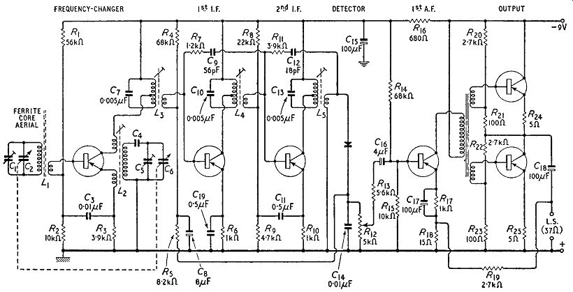
Fig. 11.13. Circuit diagram of complete single-waveband superheterodyne
transistor receiver
... but at all other frequencies there is a loss in sensitivity due to mistuning of the aerial circuit and this loss is the greater the higher the Q. value. On the other hand if the Q. is made too low there is a danger of second-channel interference. A working Q. of 100 is a reasonable compromise. The aerial coil is coupled to the base circuit of the frequency-changer by means of a secondary winding, and the inductance of this winding can be so chosen that the damping due to the frequency changer gives a working Q. of this value.
The frequency-changer circuit is similar to that shown in Fig. 11.3 but the capacitors C4 and C5 are included to permit adjustment of the frequency range covered by the receiver and to give the required 3-point tracking. With the tuning capacitors at minimum capacitance C5 is adjusted to give the required high-frequency tuning limit. With the tuning capacitors at maximum capacitance L2 is adjusted to give the required low-frequency tuning limit.
These adjustments are repeated until no further adjustment is necessary. If the value of C4 is correctly chosen, the alignment of the receiver will also be perfect at a frequency near the centre of the waveband.
In aligning the receiver the trimmer C1 is adjusted to give maximum sensitivity near the high-frequency end of the waveband and the inductance L1 is adjusted to give maximum sensitivity near the low-frequency end. The inductance can be adjusted by sliding the winding along the Ferrite rod or strip.
The remainder of the receiver is conventional, comprising i.f., detector and a.f. stages of types described earlier. One point meriting description is the decoupling network R16C15. This is particularly necessary in a receiver such as this which has a class-B output stage. The collector current of a class-B output stage is not steady but has a strong component at the second harmonic of the frequency of audio output. This current, in flowing through the internal resistance of the battery, sets up a voltage which is impressed on the collector voltage for all other stages. This can cause distortion if it affects the gains of these stages. This is particularly likely when the internal resistance of the battery rises due to ageing. The network R16C15 reduces distortion due to this cause by attenuating such voltages, the reactance of C15 being small compared with R16 at audio-frequencies.
Another interesting feature of the receiver is the small forward bias of the detector by the network R4R5R12. This is deliberately introduced to improve the performance of the detector. The characteristic of a point-contact (and a junction) diode is almost straight where it passes through the origin and detection efficiency is therefore poor for small applied voltages. The bias provided can be chosen to give maximum detector efficiency for small input signals, thus improving receiver sensitivity. Alternatively the bias can be chosen to minimize the peak-clipping which occurs for large signal inputs as a result of the difference in value of the d.c. and a.c. detector loads: this adjustment improves the quality of reproduction from local transmissions.
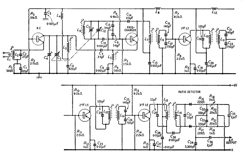
Fig. 11.14. Circuit diagram of a transistorized f.m. receiver up to the
af. output from the detector
F.M. RECEIVER
We have now discussed f.m. detectors and the use of transistors in a.f. amplifiers, i.f. amplifiers and frequency changers: we can now consider the design of a transistorized f.m. receiver.
In the first-class service area of an f.m. transmitter the field strength is greater than I m V /meter: in the second-class service area (where there may be slight interference from car ignition systems) the signal strength is between 250 µ. V /meter and 1 m V /meter.
The signal delivered to the input terminals of a receiver from a half-wave dipole aerial via a properly-matched feeder is approximately equal to half the field strength, i.e., is 125 µ.Vat the edge of the second-class service area. These signal strengths are however measured using an elevated dipole in the open air. A band-II dipole is 5 feet long and in a portable receiver (such as a transistorized receiver is likely to be) a much smaller aerial must be used: this inevitably gives a smaller signal than an elevated resonant dipole. Moreover portable receivers are likely to be used inside buildings or on the ground where the signal strength can easily be 30 dB below the values measured with an elevated resonant aerial.
Thus under unfavorable conditions the signal delivered to the aerial terminals of a portable f.m. receiver can be less than 5 µ-V. To obtain good results from an input signal as small as this, a superheterodyne receiver must be used. It is advisable, too, to employ an r.f. stage before the frequency changer: this improves signal-to-noise ratio and helps to minimize oscillator reradiation.
The r.f. stage and frequency changer are unlikely to provide a voltage gain of more than 15 and the minimum signal to be expected from the frequency changer is 75 µ.V. For reasons given earlier a ratio detector is the most likely choice and for adequate a.m. rejection this requires an input to the diodes of not less than 0.5 volt. The i.f. amplifier thus requires a gain of 7,000 and this determines the number of i.f. stages required. We have already shown that a 10.7-Mhz i.f. stage using a non-uni-lateralized drift transistor gives a voltage gain of about 10 when working into a following transistor and about 65 when working into a ratio detector. A total of three i.f. stages will therefore provide the required gain and the receiver circuit diagram up to the a.f. output from the ratio detector can take the form illustrated in Fig. 11.14.
In this the circuit arrangements of frequency changer, i.f. amplifier and ratio detector are all identical with those given earlier. The r.f. stage is a common-base amplifier which at frequencies around 100 Mhz gives as much gain as a common-emitter type. The input tuned circuit L2C1 is heavily damped by the low input resistance of the amplifier and gives so low an effective Q, value that there is no advantage in having variable tuning. If the tuning is fixed at the centre of the band to be received the loss due to this input circuit at the ends of the band is negligible.
The a.f. output from the ratio detector is small enough, when the receiver is tuned to a weak signal, to require the use of a three-stage audio amplifier. This may consist of a gain stage followed by a driver stage which in turn feeds a push-pull class-B output stage.
The receiver thus includes a total of nine transistors (five drift types and four uniform-base types) and two point-contact diodes.
Alignment
The receiver should be aligned in the following manner. With the tuning capacitors at minimum capacitance trimmer C11 is adjusted to tune in a signal at the high-frequency end of the band say at 100 Mhz. Then with the tuning capacitors at maximum capacitance L6 is adjusted to tune in a signal at the low-frequency end of the band-say at 87.5 Mhz. The adjustment of C11 is now repeated at 100 Mhz with the tuning capacitors at minimum capacitance. The adjustment of L6 is next repeated at 87.5 Mhz with the tuning capacitors at maximum capacitance and these two adjustments are repeated until no further adjustment is required.
The receiver now covers the required band. C4 is adjusted to provide maximum gain at the high-frequency end of the band and L3 to provide maximum gain at the low-frequency end of the band.
These adjustments too, are repeated until no further improvement in gain is obtainable. Finally L2 is adjusted to give maximum gain at the centre of the band-say at 94 Mhz.