Introduction
TRANSISTORS can be successfully employed in practically all thermionic-valve circuits which use triodes. For example, there are transistor discharger circuits, transistor Miller-integrators, transistor bootstrap circuits and transistor multivibrator circuits to name only a few. We cannot describe all such circuits in one short chapter but we shall describe the transistor multivibrator in some detail.
BI-STABLE MULTIVIBRATOR
The basic circuit of a bi-stable multivibrator using transistors is given in Fig. 12.1. In such a circuit, as in all relaxation oscillator circuits, the transistors are at all times in one or other of two states, that is to say either fully conducting (with collector-emitter potential nearly zero) or completely cut off (with collector current zero except for the inevitable leakage current Ic0'). The dissipation in the transistors is low in either state and there is no need for protective circuits to avoid excessive dissipation as in class-A amplifiers. The circuit of Fig. 12.1 is so arranged that when one transistor is conducting, its collector potential ensures that the other transistor is cut off. Thus the circuit has only two possible states:
(1) TR1 conducting and TR2 cut off
(2) TR2 conducting and TR1 cut off
... and the circuit is termed bi-stable because without a stimulus from an external source it will remain indefinitely in either state.
If the circuit is initially in state (1), an external signal will cause it to enter state (2) and the change of state is accomplished with great rapidity. The speed of transition is due to the positive feedback inherent in the circuit: this feedback is obvious if the circuit is regarded as that of a two-stage direct-coupled amplifier with the output voltage returned to the input. A second external signal applied to the circuit will cause it to return to state (1) again.
During these changes of state the collector potentials of TR1 and TR2 alternate between a maximum negative value when the transistor is cut off and a minimum when it is fully conducting.
If a recurrent triggering signal is applied to the circuit, the voltage waveform generated at each collector is approximately rectangular in form. Moreover, the frequency of the rectangular signal is half that of the triggering signal, enabling such circuits to be used in frequency dividers or binary counters.
Speed-up Capacitors
In the simple form illustrated in Fig. 12.1 the waveforms generated at the collectors during changes of state have poor rise times. This is because the circuit coupling each collector to the other base consists of a series resistor feeding into the parallel RC combination of the transistor input impedance. Such a network has a response which falls as frequency rises and thus the positive feedback in the circuit is more marked at low than at high frequencies. To achieve steep edges (small rise times) in the output signals the degree ...
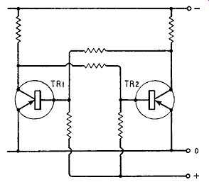
Fig. 12.1. Basic circuit of bistable multivibrator using transistors
... of feedback should be independent of frequency: thus the coupling circuits should not have a high-frequency loss. The coupling circuits can be made aperiodic (i.e. non-frequency-discriminating) by shunting the series resistors with capacitors as shown in Fig. 12.2 and the condition for an aperiodic response is that the time constant of the coupling resistor-coupling capacitor combination should equal that of the transistor input impedance. If a smaller value of capacitor is used the rise time of the multivibrator output signals is not improved as much as is possible: if a larger value of capacitor is used the negative-going changes in the collector potentials have a poorer rise time as shown by the dotted curve at the bottom centre of Fig. 12.6.
To avoid the necessity for the separate positive supply for the emitters shown in Fig. 12.1, the two emitters may be bonded and ...
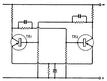
Fig. 12.2. Transistor
bi-stable multivibrator with speed-up capacitors
... connected to the earth line as shown in Fig. 12.2. In this circuit the emitter current of the conductive transistor ensures that the other is cut off by making its emitter potential more negative than its base potential. It is advisable to decouple the common emitter resistance to preserve steep edges in the output waveform.
Triggering signals applied to a bi-stable transistor circuit to interchange the states of conduction or non-conduction can be applied to the base or the emitter circuit. It is preferable, however, to apply signals to the base because this takes advantage of the ex' of the transistors to amplify the triggering signals. If pnp transistors are used, a positive-going signal is required to cut off a conductive transistor or a negative-going signal to make a cut-off transistor conductive. Of these two alternatives the first is in general preferable because it requires a smaller voltage signal, there being no large bias to overcome. Moreover, a triggering signal applied to a conductive transistor is amplified by the transistor causing a much larger triggering signal to be applied to the second transistor.
In counter circuits it is usual to inject a series of unidirectional pulses into a bi-stable circuit and some means is required of directing the pulses alternately to the base circuits of the two transistors.
One method of achieving this is by the use of the diode gate circuit illustrated in Fig. 12.3. The input signals are applied to the two capacitors C1 and C2 and then to the two base circuits via diodes DI and D2. The switching action of the diodes can be followed from the following section.
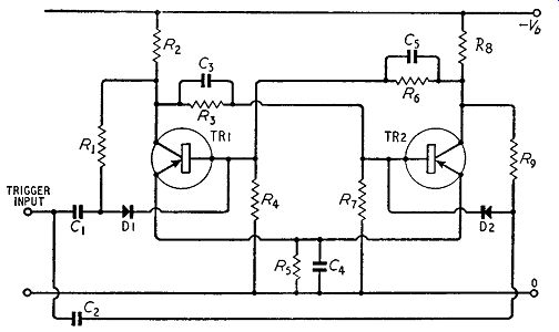
Fig. 12.3. The circuit of Fig. 12. 2 with diode triggering gate
Diode Gate Circuit
Suppose TR1 is conductive. The collector current is a maximum and the collector potential is very low (in practice commonly within 0· 1 volt of the emitter potential). The base-emitter voltage is always small and thus there is little difference between the collector and base potentials. The diode D1 is connected between collector and base (via R1) and there is little potential difference across the diode. The diode is so connected that any positive going edge applied to capacitor C1 makes the diode conduct, i.e., low-resistance and the edge is conducted to the base of TR1.
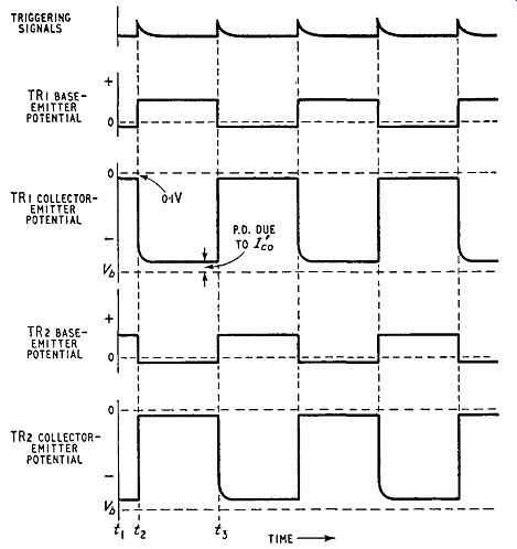
Fig. 12.4. Base and collector waveforms for the bi-stable multivibrator
of Fig. 12.3
The edge cannot, however, reach the base of TR2: this transistor is cut off and its collector current is a minimum ( consisting of leakage current Ic0' only). The collector potential of TR2 is very high and, except for the voltage drop across R8 due to leakage current would be equal to the supply voltage. There is thus a maximum potential difference across the diode D2 which is connected between collector and base (via R9 ). Moreover this potential difference biases D2 in the reverse direction so that it does not conduct when a positive-going edge is applied to C2 unless this edge has sufficient voltage to offset the static bias (and the amplitude of the edge must be controlled to avoid this). A positive-going edge applied to C1 and C2 thus reaches the base of TR1 but not that of TR2. This edge initiates the regenerative change of state characteristic of multivibrators which ends with TR1 cut off and TR2 conducting. A second positive-going edge applied to the circuit is now conducted to the base of TR2 but not to that of TR 1. This triggers off a second change of state, hastened by regeneration, which ends with TR2 cut off and TR1 conductive.
This is the state originally postulated.
Waveforms The waveforms for a triggered bi-stable multivibrator are given in Fig. 12.4. At the time t1 TR1 is conductive, the base-emitter...
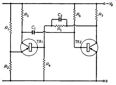
Fig. 12.5. Transistor monostable multivibrator
...potential being zero and the collector-emitter potential a minimum.
At the same instant TR2 is cut off, the base-emitter potential being positive and the collector-emitter potential a maximum. When t = t2 a triggering pulse is received by TR1 and interchanges the states. At t = t3 a second triggering edge is received (by TR2 this time) and interchanges the states again. Two triggering signals are thus required to produce one complete rectangular wave from TR1 or TR2 collector circuit.
MONOSTABLE MULTIVIBRATOR
If a coupling resistor is removed from a bi-stable multivibrator, the resulting circuit has one direct and one capacitance inter transistor coupling. Such a circuit is illustrated in Fig. 12.5. TR1 is biased by the potential divider R1R2 but TR2 has no bias components other than R6 which is returned to the negative supply line from the base.
The mode of operation of a circuit of this type is quite different from that of a bi-stable circuit and will be illustrated by reference to the waveforms given in Fig. 12.6.
At a time t1 TR2 is assumed conductive: the d.c. conditions in the circuit are such that TR1 is cut off. The circuit will remain in this state indefinitely unless it is compelled to leave it by an externally-applied signal.
Thus this state (TR2 conductive and TR1 cut off) is a stable one and is similar in nature to either of the states of a bi-stable multi vibrator.
At t2 TR1 is made conductive by applying a negative-going edge to its base or preferably (as shown in Fig. 12.6) by applying a positive-going edge to TR2 base. The collector potential of TR1 makes a positive excursion (AB in Fig. 12.6). The voltage across a capacitor cannot be changed instantaneously and this edge is transferred without loss in amplitude by C1 to the base of TR2 (ab), cutting TR2 off. The circuit is now in the second of its two possible states (TR1 conductive and TR2 cut off) but it cannot remain in it permanently because C1 begins immediately to discharge through R8 and the output circuit of TR1. As the discharge proceeds the potential at the base of TR2 becomes less positive (be) until a point (c) is reached at which TR2 begins to conduct. As soon as TR2 is conducting strongly enough for the overall gain of the two transistor stages to exceed unity, regeneration occurs and the circuit changes state rapidly leaving TR2 conducting and TR1 cut off. The circuit is now back in its stable state again.
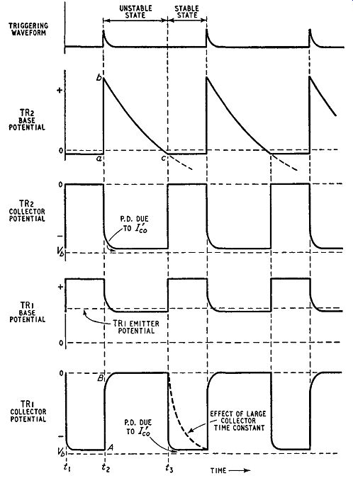
Fig. 12.6. Base and collector waveforms for the monostable multivibrator
of Fig. 12.5.
The state in which TR1 is conducting and TR2 cut off is thus an unstable state because the circuit cannot remain indefinitely in it. It will automatically revert to the stable state after an interval without the aid of external triggering signals. External signals are needed to bring about the change from the stable to the unstable state but not to accomplish the reverse change. The duration of the unstable state can be given any desired value within certain limits by appropriate choice of circuit constants.
Circuits such as this which have one stable and one unstable state are termed monostable. Their chief application is in producing accurately timed delays.
The delay is equal to the period of the unstable state and we thus need to be able to calculate the component values needed to produce a wanted delay. This can be achieved in the following manner.
Duration of Unstable State
The duration of the unstable state is equal to the time taken for the potential at the base of the non-conductive transistor to fall almost to zero.
First consider the conditions in the circuit in the stable state: TR1 is cut off and TR2 conductive. If TR1 were an ideal transistor its collector potential would be equal to that of the supply
-Vi. In practice there is a voltage drop across R3 due to the leakage current lc0' in TRI. However, provided we are prepared to accept an approximate answer we can neglect the voltage drop due to Ic0' and assume that the collector potential is - Vb. TR2 is conductive and its base potential is slightly negative with respect to earth potential: again we can take this potential as being equal to earth potential to obtain an approximate answer. Thus the voltage across C1 is equal to Vi, the right-hand plate being positive with respect to the other.
The unstable period begins when TR1 is suddenly switched on.
The collector current rises at this instant to a value which is sufficient with proper design to bring the collector potential almost to zero. This excursion is handed on to TR2 by C1 and the base potential immediately becomes + Vi. C1 now begins to discharge through Ra (and the output circuit of TR1 but the resistance of this circuit is normally small compared with Ra and will be neglected) and if the discharge were completed the base potential of TR2 would fall exponentially with time from + Vb to -Vi.
However, as soon as the base potential reaches zero (the halfway point in the discharge) TR2 begins to conduct and the unstable period is abruptly terminated.
Thus the duration of the unstable state is given approximately by the time taken for the voltage in a circuit of time constant RaC1 to fall to half its initial value. The fall in voltage is given by the equation where Vt is the voltage after an interval t and V0 is the initial voltage. This may be written in the form, from which: t = RsC1 loge Vo/Vi
The time taken for the voltage to fall to half its initial value is obtained by putting V0 /Ve equal to 2 in the above expression. We then have
t = RsC1 log0 2 = 0.6931RsC1
Thus to obtain a duration of say 1 millisecond
Any values of R6 and C1 would thus appear to be suitable provided their product (time constant) is I -44 milliseconds. In fact, if a good approximation to rectangular output signals is required, there are limitations to the values of Rs and C1 which can be used.
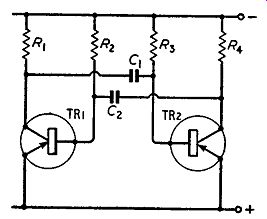
Fig. 12.7. Transistor astable multivibrator
When TR1 is cut off at the end of the unstable period, its collector potential tends to go negative. This tends to drive the base of TR2 negative but as soon as TR2 starts to conduct its input resistance becomes very low and the base potential is effectively stabilized near zero. Thus the collector potential of TR1 can go negative only by charging C1 through the load resistor Ra, The time constant RaC1 in fact determines the rise time of the voltage edge generated at TR1 collector and this edge may be used for triggering other circuits when the monostable circuit is used as a delay generator.
This edge must thus be steep and this requires a small value of time constant RaCl' (The effect of a large value of RaC1 is shown in dotted lines in Fig. 12.6.) Ra cannot be made less than a certain value, otherwise an abnormally-high value of collector current will be required to reduce the collector potential to near zero when TR1 is conducting. If the supply is -6 volts Ra can be 3 k-ohm and a collector current of 2 mA is required-a reasonable value. This is the minimum value of Ra and a short rise time can be achieved only by using small values of C1, If, however, C1 is made small, Rs must be large to give the desired value of time constant RsC1 on which the duration of the unstable period depends. Rs supplies the base current to TR2 when TR2 is conductive and this sets an upper limit to the value of Rs which can be used. For example if TR2 is to take 2 mA collector current and if 1 if 50, the base current is given by 2/50 mA, i.e. 40 µA. If the supply voltage is 6 volts R6 is given by 6/(40 x 10^-6), i.e., 150 k-O. This is the maximum permissible value and it is advisable to use a smaller value, say, 100 k-O to ensure that the collector potential is near zero when TR2 conducts. Thus the minimum value of C1 which can be used is given by
1.44 X 10^-3 C1 = -------- R6
= 1.44 X 10 3 F 100 X 10^3
= 0.014 µF
The time constant governing the positive edge developed at the collector of TR1 is given by R3C1
= 3 x 10^3 x 0.014 x 10^-6 second
= 0.042 millisec
The rise time is approximately twice the time constant and is thus less than 0.1 millisecond.
ASTABLE MULTIVIBRATORS
If both the coupling resistors are removed from a bi-stable multivibrator, the resulting circuit has two capacitance couplings.
Such a circuit has two unstable states and automatically switches from one to the other continuously without need for external triggering signals. Circuits of this type are termed astable and are free-running relaxation oscillators. They can, however, readily be synchronized at the frequency of a recurrent signal applied to them.
Fig. 12.7 gives the circuit diagram of an astable multivibrator.
No emitter bias is used and both bases are returned via resistors to the negative supply line. The behavior of the circuit will be illustrated by the waveforms shown in Fig. 12.8. At t1 TR1 is cut off by a positive signal at the base and the collector potential is a negative maximum. At the same time TR2 is conducting, having a slightly negative base potential, the collector potential being nearly zero. TR2 is in a stable state but TR1 is not, because the potential at its base is moving negatively as C2 discharges through R2. At t2 the potential at TR1 base is sufficiently negative for TR1 ...
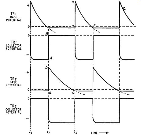
Fig. 12.8. Base and collector waveforms for the astable multivibrator of
Fig. 12.7.
... to start conducting. As explained for the monostable multivibrator, this starts a regenerative action which causes TR1 to become abruptly conductive. The resultant steep positive voltage (AB) at TR1 collector is transferred by C1 to the base of TR2 (ab), cutting TR2 off. There now follows the exponential change in base potential (be) previously described. It keeps TR2 cut off for a period given approximately by 0.69R3C1 seconds which terminates at time t3 when TR2 becomes abruptly conductive. TR2 is now in a stable state but TR1 is not, being cut off by a positive edge (de) which decays exponentially (ef). This keeps TR1 cut off for a period given approximately by 0.69R2C2. This is the circuit condition assumed initially. Thus the cycle continues, the period of oscillation being equal to the sum of the durations of the two unstable periods:
T = 0.69(R3C1 + R2C2)
If R1
= R3
=R and C1
= C2
= C the multivibrator is symmetrical and generates square waves ( equal mark space ratio) at both collectors.
The period of oscillation is given by
T = 1.38RC
The free-running frequency of such a multivibrator is given by
f=!_ T 1
--- 1.38RC
A multivibrator required to be synchronized at the line frequency (approximately 10 khz) of the British Television System would be designed to have a natural frequency somewhat lower than this say 7 khz. We have already seen that suitable values for the load resistors and base resistors are 3 k-ohm and 100 k-ohm: we have now to determine a suitable value for the coupling capacitors. From the above expression we have.
C= 11.38Rf 1
- 1.38 x 10^5 x 7 X 10^3 F
= 0.001 µF approximately
SYNCHRONIZING OF MULTIVIBRATORS
Bi-stable and monostable multivibrators are triggered by signals which cause the circuit to leave a stable state. Such a technique cannot be applied to astable circuits because these have no stable states. The synchronizing signals injected into an astable circuit are designed to terminate the unstable periods earlier than would occur naturally. It follows that the natural frequency of the circuit must be lower than the frequency of the synchronizing signals.
To terminate the unstable periods unnaturally early the synchronizing signals can take the form of negative-going pulses applied to one or both of the bases of the transistors. The amplitude of the edges is important. If the natural frequency of the multivibrator is small compared with the frequency of the synchronizing signals, a small-amplitude signal may cause the multivibrator to run at a simple fraction, say 1/5th of the sync frequency. Increase in the amplitude of the synchronizing signal may cause the multivibrator frequency to jump to ¼ of the synchronizing frequency. Further increase may cause the frequency to jump to ¼ the synchronizing frequency, etc. Thus a synchronized multivibrator can be used as a frequency divider but close control of the synchronizing signal amplitude is necessary to obtain a consistent division ratio.
HOLE STORAGE
The voltage step generated at the collector of a transistor is steeper when the transistor is abruptly turned on than when it is turned off. One reason for this has already been suggested: when a transistor is cut off the collector potential can only change at the rate determined by the time constant of the collector load resistance and the following coupling capacitor. When the transistor is turned on, however, the state of charge of the coupling capacitor is not altered and the step can thus be very steep.
There is, however, another effect which tends still further to degrade the rise time when the transistor is cut off. This is an effect, internal to the transistor, which causes the collector current to persist for a few microseconds after the emitter current has been cut off. This occurs in transistors which have been driven hard into conduction so that the collector-emitter potential is nearly zero.
In these circumstances the emitter injects more current carriers (holes in a pnp transistor) into the base region than are required to give the collector current and the excess carriers are stored ready to be swept into the collector region to prolong the collector current for a short period after the emitter current has been cut off. This hole-storage effect can be avoided by so designing the circuits that the collector-emitter potential does not approach zero but is limited to a value such as 1 volt: this can be achieved by use of diodes.