Introduction
THE small-signal amplifiers described in Chapter 7 are designed to produce a voltage or a current output. When a voltage output is wanted, the magnitude of the current output is usually of little consequence provided the final transistor can supply it without distortion. Similarly if the amplifier is designed to supply a current output, the magnitude of the voltage output is of secondary importance provided it is not sufficient to cause overloading and consequent distortion. In general the output, whether of voltage or of current, is small compared with the maximum that the transistor could supply and there is little danger of overloading.
In this chapter we shall discuss large-signal amplifiers and here the design principles are quite different. A power output is now required and the voltage swing and the current swing of the amplifier are both of importance. Moreover there is a very real danger of overloading and a major problem is how to obtain the maximum output from a given transistor without distortion.
The final stage of a large signal amplifier may operate in class A or class B and can give an efficiency much higher than is obtainable from a large-signal valve amplifier.
CLASS-A AMPLIFIERS
The circuit of a class-A output stage is given in Fig. 10.1. For maximum efficiency full advantage must be taken of the available collector-current and collector-voltage swing: that is to say, the load resistance and input-signal amplitude must be so chosen that the collector voltage and collector-current swing between zero and twice the quiescent (no-signal) value.
Suppose the battery voltage is Vb and the steady collector current in the absence of an input signal is fc. Then the power taken from the battery is Vb_Ic and most of this is dissipated as heat in the transistor. This static dissipation must not exceed the maximum value quoted by the manufacturers. If a sinusoidal input signal is applied to the transistor, power is supplied to the load but the power taken from the battery remains constant because no change…
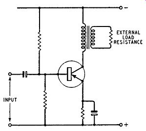
Fig. 10.1. Essential features of a single-ended class-A transistor output
stage.
… has taken place in the average or d.c. component of the collector current.
It follows that the power dissipated in the transistor becomes less when the input signal is applied. If, therefore, the transistor does not become too hot in the absence of an input signal, there will be no danger at all of damaging it by heat when the signal is applied.
When the transistor is delivering its maximum undistorted power, the peak value of the collector voltage is nearly equal to Vb and the peak collector current is le, The output power is obtained by multiplying the r.m.s. collector voltage by the r.m.s. collector current: for a sinusoidal output signal these are Vb __/2 and Ie/__/2 and thus:
. vb le
maximum power output = V2
. V2
_ V~e
--2
The power taken from the battery is V~e and thus the efficiency is 50 percent.
This is the theoretical maximum and in practice a transistor class-A stage can approach it very closely. This efficiency applies only for sinusoidal signals and when the transistor is driven to the limit of its output power. For smaller input signals the efficiency is less.
The amplitude of an a.f. signal varies over a range depending on the nature of the signal. For orchestral music the range between the maximum and minimum amplitudes may be as much as 40 dB. For jazz and speech the range is much less.
It can therefore be seen that the efficiency of a class-A amplifier with an a.f. input varies from instant to instant and the average efficiency is in actual practice much less than the theoretical maximum of 50 percent.
As can be seen from Fig. 10.2 the slope of the load line for maximum power output is given by Vb/le: this is then the value of the optimum load resistance.
As a numerical example, consider a transistor rated for 100 mW maximum collector dissipation and operating as a class-A output stage from a 6-volt supply.
The maximum undistorted output power is 50 mW and the mean collector current le is given by le X 6 100 X 10^-3 le 100 X 10^-3 A 6 17 mA Rz Vb
- le 6 17 X 10^-3 ohms
= 350 ohms
One practical point is that the battery voltage must exceed 6 volts to give a 6-volt swing of collector potential. This is because the steady voltage across the emitter resistor, the primary resistance and the transistor knee voltage must be subtracted from the battery voltage to give the effective collector-emitter voltage.
The output transformer must match the optimum load to the load resistance. Therefore, if the load resistance is 3 ohms,
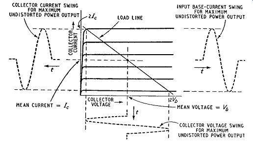
Fig. 10.2. Conditions in a class-A transistor output stage.
the transformer must have a ratio of:
__/(350/3): 1 = _/117: 1
= 11 : 1, approximately
The primary inductance determines the low-frequency response which is 3 dB down at the frequency for which the inductive reactance is equal to the optimum load. In an a.f. amplifier the 3 dB loss frequency may be 50 hz and we have:
2 pi f L = R
R L= 2Trj 350
- H 6·28 X 50
= l·l H
The transformer should have a primary inductance of this value with 17 mA direct current flowing.
Two transistors may be operated in class-A push-pull and a typical circuit is given in Fig. 10.3. The collector-to-collector optimum load is twice that for a single class-A transistor and the output transformer needs twice the primary inductance. Its design is simpler, however, because it is not polarised, the d.c. components of the collector currents flowing in opposite directions in the two halves of the primary winding.
CLASS-B AMPLIFIERS
In a class-B amplifier the base is biased almost to the point of collector current cut-off. In the absence of an input signal, therefore, very little collector current flows but the current increases ...
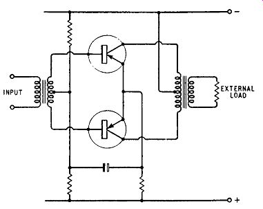
Fig. 10.3. Circuit for a push-pull class-A transistor output stage.
... as the amplitude of the input signal increases. This leads to economy in running costs because the current taken from the battery tends to be proportional to the signal amplitude and not independent of it as in a class-A amplifier. Positive half-cycles of the input signal are, however, not reproduced in a single class-B amplifier and it is essential to use two transistors in push-pull.
Such a pair of transistors can give a power output of 2·5 times the maximum permissible collector dissipation of the two transistors: this is 5 times that available from the same two transistors operating in class-A push-pull. This may be shown in the following way.
Let the peak collector current of each transistor be Ip and the battery voltage Vb. Then the peak collector-voltage swing Vp is equal to Vb. The power output from a push-pull stage is given by the product of the r.m.s. collector current (/p/,V2) and the r.m.s. collector voltage (Vp/y2) and is thus given by I_p V_p / 2.
If the input signal is sinusoidal, the combined collector current is sinusoidal in waveform as pictured in Fig. 10.4. Such a wave form has a mean value, or d.c. component, equal to 2/ pi of the peak value (I_p) and the power taken from the battery is thus equal to 2V_b l_p/ pi , giving the efficiency as:
This is the maximum efficiency of which the stage is capable and to obtain it the optimum load per transistor must be equal to…
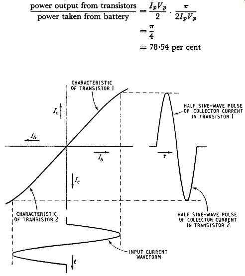
Fig. 10.4. Operation of a push-pull class-B transistor amplifier (peak voltage)/(peak
current). For a class-B push-pull the collector to-collector load is given
by 4Vp/lp.
If the load and battery voltage are kept constant and the input signal amplitude is reduced, the efficiency falls linearly due to the increasing failure to make use of the voltage swing available. This is easily shown. Suppose the input voltage is reduced to a times the value which gives maximum output. Then the collector current swing falls to alp and (since the load is constant) the collector-voltage swing falls to a Vp, giving the power output per pair of transistors as a2IpVp/2. The mean value of the collector current is now 2alp/1T and the power taken from the battery is 2alp Vp/1T. The efficiency for the reduced input signal is given by:
power output from transistors_ a2IpVp 1T power taken from battery - --2- 2alpVp 1T
=a. – 4
The efficiency is thus directly proportional to the input signal amplitude.
In transistor amplifiers we are particularly interested in the power Pt dissipated in the transistors themselves, for it is this which causes heating of the junctions and can damage them.
Now power dissipated in transistors i.e., Pt
Differentiating this:
power taken from battery 2alpVp 1T dPt = 2IpVp _ alpVp da 1T
Equating this to zero to find the maximum,
2 a= 1T power output
The heat in the transistors is thus a maximum when the signal amplitude is 2/7T (approximately 0·63) times that giving maximum output power. Substituting this particular value of a in the general expression given above we have a21 V power output from amplifier = ____E__£ 2
_ 2IpVp
-~ power taken from battery = 2alpVp Tr
By subtraction, d
. . d. . 2lpVp power dissipate m transistors= - 7r2
These results show that this particular value of a makes the power output one-half that taken from the battery: in other words it coincides with an efficiency of 50 percent. The maximum power output from the class-B pair is lpVp/2. The maximum power dissipated in the transistors is 2lp Vp/Tr 2.
The ratio of these two quantities is Tr 2/4, approximately 2.5 : 1, showing that it is possible to obtain an undistorted output of 2.5 times the rated maximum collector dissipation of the two transistors, i.e., 5 times the maximum collector dissipation of one of them. This applies only for a sinusoidal input.
As a numerical example, consider two transistors each with a maximum collector dissipation of 100 mW. In class-B push-pull it is possible to obtain from these an output power of 500 mW. If the battery supply is 6 volts, this is also the peak value of the collector voltage, and the peak current is given by Ip where:
1 P = 2 Vplp 2P lp= Vp
= 2 X 500 mA 6
= 170 mA
approximately
The collector-to-collector load is given by Ri = 4Vp Ip 4 X 6
----- 170 X 10^-3 ohms
= 140 ohms approximately
Driver Stage
The transistor feeding a class-B output stage may be regarded as a large-signal amplifier because it must supply appreciable power to the base circuits of the output stage. The design of the driver stage and the transformer coupling it to the output stage depends on the input resistance of the output stage.
We have so far assumed the input resistance of a common emitter amplifier to have a value determined by the transistor parameters and the output load resistance. For small input signals this is a reasonable assumption, and the input resistance is commonly taken as 1 k-O. A class-B stage, however, does not satisfy these conditions: it is biased almost to collector-current cut off and, in the absence of an input signal, has an input resistance higher than that of a class-A amplifier. A class-B stage requires a large input signal to swing the collector current to its maximum limit and for such signals the input resistance is less than that of a class-A amplifier.
Thus the input resistance is no longer a constant but varies with the input signal amplitude, decreasing as the input signal increases. The variation may be from, say, 2 k-O for small signals to 200 ohms for large signals. This variation of input resistance can be anticipated from inspection of the current-input voltage characteristic for a junction transistor (Fig. 1.12). The slope is small near the origin but increases as the input voltage is increased.
The input resistance is measured by the reciprocal of the slope and decreases as signal amplitude increases.
These variations in input resistance can, unless precautions are taken, cause serious distortion. For example, suppose the output stage is driven from a signal source having an output resistance small compared with the minimum input resistance of the output stage. This means that the signal voltages applied to the bases of the output stage are nearly equal to that of the signal source and are therefore substantially undistorted. If the input resistance of the output stage were constant and independent of signal amplitude the input current would also be undistorted. The input resistance does, however, vary with signal amplitude. Thus the input current is not linearly related to the signal voltage and must be distorted.
Transistors are, of course, current-operated devices and if the input current is distorted, the output current must also be distorted.
The distortion obtained in this mode of operation (called constant voltage operation) is most unpleasant: for small signals the input resistance is large and the input current is smaller than required for distortionless amplification. Thus a sine-wave input voltage is reproduced with a waveform similar to that shown in Fig. 10.5.
This is known as cross-over distortion because it occurs when one transistor is being cut off and the other turned on, i.e. when the
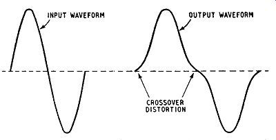
Fig. 10.5. Input and output waveforms for an amplifier giving cross-over
distortion state of conduction is being handed over from one transistor to
the other.
To reduce cross-over distortion, the input current for the output stage must be undistorted. The variations in input resistance must therefore have no effect on the input current. To achieve this the output stage must be driven from a high-resistance signal source.
Ideally the source resistance should be large compared with the highest value of input resistance likely to occur: we then have constant-current operation. If, however, the driver transformer is designed to satisfy this requirement, the gain of the driver stage is low. This difficulty can be reduced by arranging that the output transistors are not biased to cut off in the absence of a signal but take a small collector current. Thus the transistors operate in class A for small input signals and the variations in input resistance are reduced. It is now possible to use a smaller value of source resistance while still avoiding the worst effects of cross-over distortion and reasonable gain is possible from the driver stage.
For transistors rated for 100 mW maximum collector dissipation, the input resistance falls to approximately 100 ohms at minimum and is probably around 1 k-O for a standing collector current of 2 mA, a typical value for a class B output stage. If high gain is essential from the driver stage and a little distortion can be tolerated, the driver transformer can be designed to match the output resistance of the driver stage (say 30 kO) to the maximum value of the input resistance (1 k-O). The turns ratio (primary to each secondary winding) required is thus:
,v(30,000/l,000) : 1 = \130 : 1
= 5.5: 1
When better quality is required and a little gain can be sacrificed, this ratio is sometimes decreased to 3 :1 or even 2:1 to give a better approximation to constant-current input for the class B stage.
Symmetrical Class-B Amplifier
The circuit of the driver stage and class-B output stage of an amplifier is given in full in Fig. 10.6. The driver stage operates in class A and the collector current is stabilized at, say, 3 mA by ...
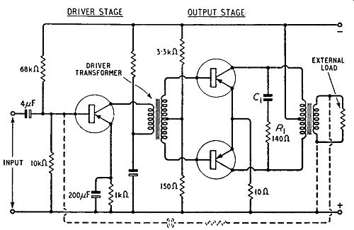
Fig. 10.6. Circuit for a driver and a symmetrical class-B output stage.
Dotted lines show how negative feedback can be applied when the driver stage
has a current input.
... the potential-divider method. A similar technique is applied to the output stage which has a common emitter resistance, the potential divider being adjusted to give the required standing collector current. The emitter resistance of a class-B amplifier cannot be decoupled because the mean emitter current is not constant (as in a class-A amplifier) but varies over a wide range depending on the instantaneous amplitude of the input signal.
A capacitor in parallel with the emitter resistor would acquire charge on current peaks and discharge in the intervals between peaks, thus introducing unwanted exponential signals into the amplifier. The emitter resistance must therefore be kept small to minimize the negative feedback which would reduce the gain of the output stage.
The emitter resistance is commonly as low as 5 ohms: nevertheless, it gives some measure of stabilization of the standing collector current and it helps to equalize differences in parameters of the two output transistors. Another resistance which must be small is the lower arm of the potential divider feeding the bases of the output transistors. The input currents of the output stage flow in this resistor and a large value would severely reduce the signal input to the output stage: a value as low as 120 ohms is commonly used. It is not advisable to decouple this resistance by a low reactance capacitor because on large input signals the capacitor becomes charged by the unidirectional input current flow for the output stage and on small input signals it discharges through the resistance, this also superimposing unwanted exponential signals on the input to the output stage.
Class-B output stages tend to give unwanted ripples on the output signal: these are caused by ringing of the secondary winding of the driver transformer when the associated transistor is cut off.
This tendency can be reduced by so constructing the transformer that the two secondary windings are closely coupled, e.g., by winding the secondaries in a bifilar manner. This discourages ringing because the undamped secondary winding is effectively damped by its close coupling to the damped winding. The net work R1C1 is included to attenuate unwanted high-frequency components such as harmonics of the input signal or oscillations due to ringing. This network together with the leakage inductance L of the output transformer and the resistance Ri of the external load form an LCR combination. Such a network can give an input resistance independent of frequency if the product R1 Ri is made equal to L/C. Distortion introduced by the class-B output stage can be reduced by negative feedback. The feedback voltage can be taken from the secondary winding of the output transformer and applied to the driver stage. It should be applied to the base if the driver stage is required to operate with a current input, and to the emitter if the driver stage is required to operate with a voltage input.
The latter alternative is preferable if the driver stage directly follows a detector, as may occur in a receiver. The degree of feedback which can be applied is limited by the phase shifts introduced by the driver and output transformers at the extremes of the passband and in l practice rarely exceeds 6 dB: even this small degree halves the harmonic distortion of the amplifier.
Asymmetric Class-B Amplifier
An interesting variant of the class-B push-pull circuit is the so-called single-ended or asymmetric circuit illustrated in Fig. 10.7.
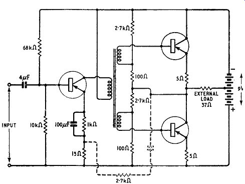
Fig. 10.7. Circuit for a driver and asymmetric class-B output stage. Dotted
lines show how negative feedback can be applied when the driver stage has
a voltage input.
The output transistors are connected in series across the collector supply battery and the load resistance is connected between their junction and a centre tap on the battery. Separate secondary windings are required for the two bases because there is now a difference in the steady voltage of the two. The load resistance equals (peak collector voltage swing)/(peak collector current swing), and for output transistors operating from a 4.5-volt supply and taking a peak collector-current of 120 mA may be as low as 37 ohms. A loudspeaker speech coil can readily be wound to have an impedance of this value and thus there is no need for a loudspeaker matching transformer: this is one of the great advantages of this circuit. It does, however, require a collector supply of higher voltage than a symmetrical circuit and the input transformer must have isolated secondary windings. The elimination of the output transformer is a great asset, however, and makes this circuit particularly suitable for miniature receivers. The use of a centre-tapped battery (as in Fig. 10.7) is not essential. The external load may alternatively be returned to the positive battery terminal (usually at earth potential) provided a capacitor is connected in series with the load to avoid disturbance of d.c. conditions. In an a.f. amplifier employing a 37-ohm load, the capacitance should be not less than 100 µ-F to avoid loss of bass.