Introduction
IN the two previous chapters we have discussed the mechanism of operation of junction transistors. We have shown that they can be used to amplify signals and have calculated the voltage gain and power gain of which they are capable. These quantities were calculated in terms of the emitter-base input resistance, the collector base output resistance and the current amplification factor. however, in designing practical transistor amplifiers and in calculating the gain likely to be achieved, we must know the electrical characteristics of the transistor in greater detail.
In this chapter we shall discuss the parameters of a transistor and will derive an equivalent circuit which can be used to calculate the input and output resistances and the gain of the various types of transistor amplifier.
COMMON-BASE, COMMON-EMITTER AND COMMON-COLLECTOR AMPLIFIERS
A transistor has three terminals, one connected to the emitter, another to the base and the third to the collector. When the transistor is used as an amplifier, the input signal is applied between one pair of terminals and the output signal is taken from another pair.
It follows that one terminal must be common to the input and output circuits.
For example in the transistor amplifiers discussed in the previous chapter it was assumed that the input signal is applied between emitter and base and that the output signal is generated between collector and base. A simplified circuit illustrating a pnp junction transistor used in such an amplifier is given in Fig. 3.1 (a). The base terminal is common to input and output circuits and such amplifiers are referred to as common-base or less correctly earthed-base amplifiers.
The common-base amplifier is, however, not the only possible arrangement. Alternatively, with the input signal still applied between the emitter and the base, the output signal can be taken between collector and emitter as shown in Fig. 3.1 (b). This illustrates the common-emitter oc earthed-emitter circuit, probably the most widely used of all transistor amplifier circuits.
A third possible arrangement is that illustrated in Fig. 3.1 (c) which shows the input signal applied between base and collector
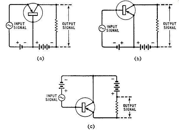
Fig. 3.1. The three basic forms of transistor amplifier: (a) common-base,
( b) common-emitter, and ( c) common-collector and the output signal generated
between collector and emitter.
This is the common-collector or earthed-collector circuit.
EQUIVALENT CIRCUIT OF A TRANSISTOR
The calculations on the common-base amplifier in the previous chapter were carried out in terms of the emitter-base input resistance Ti, the collector-base output resistance r0, and the current amplification factor o:. The input and output resistance values and the current amplification factor assumed for these calculations do not apply to the common-emitter or the common-collector amplifiers and to perform calculations on these amplifier types we need to know their values of input resistance, output resistance and current amplification factor.
Alternatively, the performance of any kind of transistor circuit, not only the three basic amplifier circuits but other circuits such as those of oscillators and trigger circuits, can be carried out by first deriving the constants of a network which has a behavior similar to that of the transistor. By applying Kirchhoff's laws or other network theorems to this equivalent circuit we can calculate the performance of the circuit.
A number of equivalent networks for a transistor have been suggested and several different parameters for expressing transistor properties have been developed including the so-called h or hybrid parameters and the r parameters (which include the input and output resistances used earlier) but in this book we shall represent the transistor as a T-network of resistances as shown in Fig. 3.2.
The transistor cannot, however, be perfectly represented by three resistances only because such a network cannot generate power (as a transistor can) but can only dissipate power. In other words the network illustrated in Fig. 3.2 is a passive network and to be accurate the equivalent network must include a source of power, i.e. must be active.
The source of power could be shown as a constant-current source connected in parallel with the collector resistance Tc as in Fig. 3.3 (a) ...
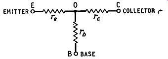
Fig. 3.2. A three-terminal passive network which can be used to build an
equivalent circuit for a transistor
... and the current so supplied is, as we have already seen, equal to a_ie, where a is the current amplification factor of the transistor and ie is the current in the emitter circuit, i.e. in the emitter resistance re. Alternatively-and this is more convenient for calculation purposes-the source of power can be represented as a constant-voltage generator connected in series with re as shown in Fig. 3.3 (b). Such a voltage has precisely the same effect as the constant current generator, provided the voltage is given the correct value, and the value required is equal to alpha_ierc as can be shown by applying Thevenin's theorem to Fig. 3.3 (a). In some books on transistors the voltage generator is given as rmie, where rm is known as the mutual or transfer resistance*

Fig. 3.3. A three-terminal active network which can be used as an equivalent
circuit for a transistor (a) including a constant-current generator, and
(b) a constant-voltage generator.
... and is equal to alpha_rc. The mutual resistance may be defined as the ratio of the e.m.f. in the collector circuit to the signal current in the emitter circuit which gives rise to it. This may be regarded as the dual of the mutual conductance gm of a thermionic valve which is defined as the ratio of the current in the anode circuit to the signal voltage in the grid circuit which causes it.
This comparison is useful because it again reminds us that the transistor is a device operated by an input current rather than an input voltage.
This network is quite satisfactory for calculating the performance of transistor amplifiers at low frequencies such as audio amplifiers because the reactances of the internal capacitances have in general negligible effects on performance.
At higher frequencies, however, and in particular at radio frequencies, it is necessary to include such capacitances in the T-network to obtain accurate answers.
Values of re, Tb, and re for Junction Transistors
The values of re, rb and re, the three resistances constituting the equivalent network of a transistor, cannot be measured directly because it is impossible to obtain a connection to the centre point 0
* The word " transistor" is, in fact, derived from " transfer resistance".
(Fig. 3.3), but their values can be deduced from measurements made at the terminals. Typical values for these resistances and also for the current amplification factor for junction transistors are as follows:
25 ohms
300 ohms
emitter resistance re
base resistance r_b collector resistance
r c current amplification
factor alpha megohm 0.98
These resistance values are those which apply when the transistor is handling a small alternating signal. They are differential or a.c. quantities and depend on the d.c. conditions in the transistor.
If the steady emitter bias current or the collector bias current are changed, the values of re, r_b and re will, in general, also change.
COMMON-BASE AMPLIFIER
A simplified circuit of a transistor common-base amplifier is given in Fig. 3.4 (a) in which R8 represents the internal resistance of the signal source and Ri represents the collector load for the ...
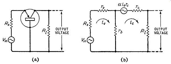
Fig. 3.4. Simplified circuit of a common-base amplifier (a), and its electrical
equivalent ( b)
... amplifier. For the sake of simplicity, methods of applying bias are not indicated.
Fig. 3.4 (b) represents the same circuit in which the transistor is represented by its equivalent T-section network. The directions of the currents in the two meshes of this network can be determined by considering the physical processes occurring in a transistor.
From Chapter 2 we know that the emitter current ie is equal to the sum of the collector current ic and the base current ib, If, therefore, ie and ic are given clockwise directions as shown in Fig. 3.4 (b), then the current in rb is (ie - ic) which is equal to ib: all conventions are therefore satisfied in this diagram. By applying Kirchhoff's laws to this circuit we can calculate the performance of the amplifier. The features of the amplifier in which we are principally interested are the following:
(a) input resistance
(b) output resistance
( c) voltage gain.
Input Resistance
Applying Kirchhoff's laws to the circuit of Fig. 3.4 (b) we have:

.... (1)
.... (2)
To obtain an expression for the input resistance we can eliminate ic between these two equations to obtain a relationship between ie and Vin.
From (2)
Substituting for ic in ( 1)
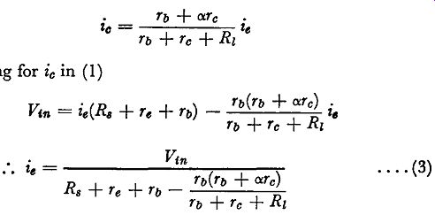
(3)
If we represent the input resistance of the transistor by Tf the circuit of Fig. 3.4 (b) takes the form shown in Fig. 3.5.
For this circuit we have:

.... (4)
Comparing expressions (3) and (4)

.... (5)
.... (6)
Expressions (5) and (6) give the value of the input resistance in terms of the emitter resistance, base resistance, collector resistance, load resistance and current amplification factor. One respect in which the transistor differs from the valve is that the input resistance depends on the load resistance, this bearing out the internal Fig. 3.5. Circuit illustrating the meaning of input resistance feedback of the transistor mentioned earlier. For a given transistor operating under constant d.c. conditions, r b, Te, Tc and o: are constant, and rt therefore depends solely on R1, increasing as R1 increases.
The range of input resistance can be calculated from expression (5). First consider expression (5) when R1 is made vanishingly small
+ Tb(Tb + O'.Tc)
rt = re rb - ---- Tb + Tc
Now for junction transistors re and alpha_rc are both large compared with rb and the input resistance is approximately given by
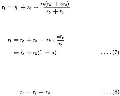
.... (7)
and this gives the value of the input resistance of the common-base amplifier when the output terminals are short-circuited.
Now consider the input resistance when Ri is made very large.
The final term in expression (5) vanishes leaving
.... (8)
which gives the value of the input resistance when the output terminals are open-circuited.
Input Resistance for a Junction Transistor as Common-base Amplifier
To obtain an estimate of practical values of input resistance for a junction transistor we can substitute re = 25 ohms, rt, = 300 ohms and ex= 0·98 and from (7) we find that the input resistance for short-circuited output terminals is given by:
r, = 25 + 300 (1 – 0.98)
=25 +6
= 31 ohms
From (8) the input resistance for open-circuited output terminals is given by re= 25 + 300
= 325 ohms
Thus the input resistance of a junction transistor used as a common-base amplifier varies between a minimum value for 350
LOAD RESISTANCE (OHMS)
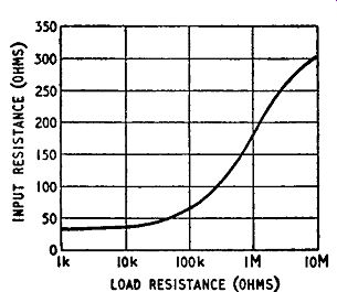
Fig. 3.6. Variation of input resistance with load resistance for a common-base
amplifier short-circuited output terminals to a maximum value for open circuited
terminals. The dependence of input resistance on output load is illustrated
in Fig. 3.6.
Output Resistance
To obtain an expression for the output resistance of the common base amplifier we can eliminate ie between equations (1) and (2)
to obtain a relationship between ic and Vin-
From (2)
Substituting for i, in ( 1)

.... (9)
If we represent the output resistance of the transistor amplifier by r O the circuit of Fig. 3.4 (b) has the form shown in Fig. 3.7.
For this circuit we have
. V Z2 =-- Rz + To

.... (10)
Comparing expressions (9) and (10) we have that V, the e.m.f.
effectively acting in the output circuit, is given by and the output resistance is given by

.... ( 11)
.... (12)
This expression shows that the output resistance depends on the source resistance R8 as well as on the base resistance, emitter resistance, collector resistance and current amplification factor. For a given transistor operating with fixed d.c. conditions, rb, re, re and o: are fixed and r O then depends on Ra, increasing as Ra is increased.
The range over which r0 varies can be estimated as follows.
First let Ra = 0. Expression (12) then becomes
re - reo: ro = re + Tb . -- re+ rb which, if the relatively small term rbre/re is neglected, gives

.... (13)

Now let Ra approach infinity. The final term in expression (11)
then vanishes, leaving the output resistance as ro =re+ Tb .... (14)
Output Resistance of a Junction Transistor as Common-base Amplifier
To obtain a numerical estimate of the range of output resistance for a junction transistor letre= 25 ohms, rb= 300 ohms, re= 1 megohm and alpha = 0.98. Substituting these values in expression (13) we iz Fig. 3. 7. Circuit illustrating the meaning of output resistance find the output resistance for short-circuited input terminals 1s given by:
The output resistance for open-circuited input terminals is, from (14), given by:
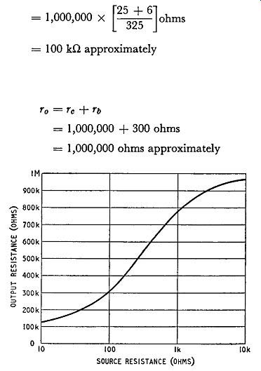
Fig. 3.8. Variation of output resistance with source resistance for a common-base
amplifier.
The variation of output resistance with source resistance for a common-base amplifier is illustrated in Fig. 3.8.
Voltage Gain
From Fig. 3.4 (b) we can see that the output voltage is given by ieRz. The voltage gain Vout/Vin is hence equal to icRi/Vin
From (9)
ic is given by
----------
Hence:

(15)
which shows how the gain is related to Ri, R,, Te, Tb, Tc and o:. The dependence of the voltage gain on the value of Ri is illustrated in Fig. 3.9, which shows gain increasing with Ri, linearly for small:
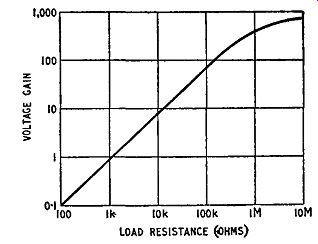
Fig. 3.9. Variation of voltage gain with load resistance for a common-base
amplifier values of Rl but becoming asymptotic to a limiting value of gain
as Rl becomes large. The shape of the curve is, in fact, the same as that
relating gain to load resistance for a thermionic valve.
For a junction transistor Tc is normally large compared with all other resistances in the expression, and it is possible to simplify expression (15) as follows :
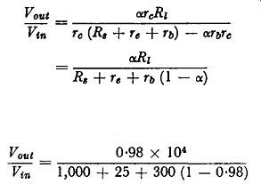
.... (16)
As a numerical example suppose …
Substituting r, for re + rb ( 1 -alpha_) in expression (16) (see Equation 7) we have for small values of Rl:
V out o:Rz Vin - R, + r, and if R8 = 0 we have Void Ri
-=ex. Vin r, which confirms the result used in Chapter 2.
To obtain an impression of the limiting value of voltage gain available from a junction transistor, suppose Ri is made large compared with re, With a few other simplifications expression (15) now reduces to the form:
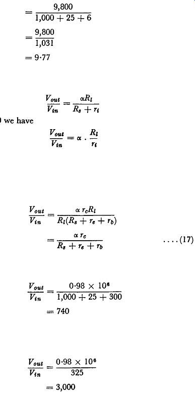
.... (17)
Substituting alpha = 0·98, Tc = 1 Mn, Rs = 1 kn, Tz = 25 ohms and Tb = 300 ohms we have that the maximum stage gain is given by:
Vout _ 0·98 X 101 Vin - 1,000 + 25 + 300
= 740
Expression ( 17) shows the importance of the source resistance R, in such determinations. If this could be reduced to negligible pro portions relative to the values of Te and Tb, the stage gain rises to:
Vout _ 0.98 X 10^6 Vin - 325
= 3,000
PRACTICAL CIRCUIT FOR A COMMON-BASE AMPLIFIER
Fig. 3.10 gives the circuit of a small-signal amplifier using a pnp junction transistor as a common-base amplifier. The base is earthed and two batteries are employed, one of 6 volts to bias the collector negatively and the other of l ·5 volts to bias the emitter positively.
Approximate values for the components used may be calculated in the following way. A suitable value for the collector voltage
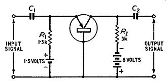
Fig. 3.10. Circuit for small-signal common-base transistor amplifier in
the absence of an input signal is -3 volts, for this permits excursions of
collector voltage during amplification up to 3 volts in peak value. Under
quiescent conditions there is a 3 volt drop in voltage across the collector
load resistor. A suitable value of steady collector current is 1 mA and from
Ohm's law the value of the load resistance is given by 3 / ( 1 x 10^-3),
i.e. 3 k-ohm.
The steady emitter current in the absence of an input signal will be just over 1 mA but can be taken as 1 mA to give an approximate value for the emitter bias resistor. The emitter bias voltage is 1.5 and from Ohm's law the resistance of the emitter circuit to give a current of 1 mA is 1.5/(1 x I0-3), i.e., 1.5 k-o. The d.c. emitter-base input resistance will contribute a few hundred ohms towards this and an emitter bias resistance of 1.3 k-ohm will be suitable.
The capacitance C1 depends on the lowest frequency it is required to amplify. For an audio-frequency amplifier this may be 50 hz.
The a.c. emitter-base input resistance shunts R1 giving an effective input resistance of say 40 ohms (see Fig. 3.6). If the reactance of the capacitor is made equal to 40 ohms at 50 hz, there is a loss of 3 dB at this frequency. The capacitance C1 necessary is given by:
I C1=- 2 pi fX
where X 1s the reactance.
Substituting f = 50 and X = 40 we have:
C1= 2 X 1 3 · 142 X 50 X 40 F
= 80 µ.F
In practice the source of input signal will have some resistance and this will permit the use of a lower capacitance for C1.
The capacitance C2 depends on the resistance which is to be connected across the output terminals.
COLLECTOR CURRENT - COLLECTOR VOLTAGE CHARACTERISTICS FOR COMMON-BASE CONNECTION
The operation of a circuit such as that of Fig. 3.10 can be illustrated by means of collector current - collector voltage characteristics.
These are usually obtained by plotting the collector current against the collector voltage for a fixed value of emitter current and the resulting curves have the form shown in Fig. 3.11. The curves are plotted in terms of input current because the transistor is a ...
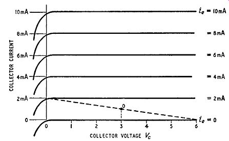
Fig. 3.11. Typical collector current-collector voltage characteristics for
a junction transistor.
... current-operated device, and the curves show that the collector current is always slightly less than the emitter current.
The characteristics have a shape similar to that of the anode current - anode voltage curves for a pentode, the horizontal portions indicating the high collector a.c. resistance of the junction transistor. However, they represent a better approximation to the ideal characteristic than those of a pentode because the transistor characteristics have no knee to limit the swing of collector potential during amplification. The collector voltage can swing the whole extent of the collector supply voltage, giving the transistor an efficiency equal to the theoretical maximum. The load line shown superimposed on the curves illustrates operation of the amplifier of Fig. 3.10. The quiescent point O corresponds to half the collector supply voltage. The position of O relative to the characteristics gives the emitter current: the bias voltage together with the external emitter resistance (R1 in Fig. 3.10) must be chosen to give this value of current.
Power Gain
The current gain alpha for a common-base amplifier is nearly equal to unity and the power gain is thus nearly equal to the voltage gain as shown on p. 31. A typical value for the voltage gain is 100 and this is also a typical value for the power gain (20 dB).
COMPARISON BETWEEN COMMON-BASE TRANSISTOR AMPLIFIER AND COMMON-GRID THERMIONIC-VALVE AMPLIFIER
An increase in the positive bias applied to the emitter (Fig. 3.10) gives a larger emitter current and hence a larger collector current.
This increases the voltage drop across the collector load resistor.
The collector bias is negative and this increased voltage drop makes the collector voltage less negative, i.e. more positive. Thus a positive voltage applied to the emitter results in a magnified positive pulse appearing at the collector: there is hence no phase inversion in a common-base transistor amplifier.
The behavior of the transistor amplifier is in fact similar to that of a common-grid thermionic-valve amplifier. The input signal is applied to the cathode circuit, which presents a low input resistance, and the output signal is taken from the anode circuit which has a much higher output resistance. The relative resistances are hence of the same order as those of the common-base transistor amplifier. A positive pulse at the cathode of the valve reduces the anode current causing the anode voltage to rise: thus there is no phase inversion in a common-grid amplifier.