Introduction
IN the previous chapter we examined the common-base amplifier, a circuit arrangement characterized by very low input resistance, very high output resistance and less than unity current gain. Input resistances vary from 30 ohms to 300 ohms; output resistances range from 100 k-ohm to 1 megohm. A noteworthy feature of the common-base amplifier is that the output signal is in phase with the input signal.
The majority of transistor amplifiers are, however, of the common emitter type and we shall now analyze the performance of this...
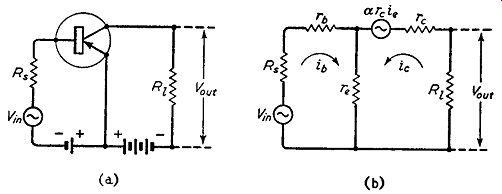
Fig. 4.1. Basic form of common-emitter amplifier (a), and its equivalent
circuit (b)
...circuit to account for its popularity. As before we shall do this by deriving expressions for the input resistance, output resistance and voltage gain.
The basic circuit for a common-emitter amplifier is given in Fig. 4.1 (a), in which R8 is the resistance of the signal source and Rz is the collector load resistance. Fig. 4.1 (b) gives the equivalent circuit in which the transistor is represented by the T-network of resistances re, rb and re introduced in the previous chapter. If the base current ib is shown acting in a clockwise direction and the collector current ic in an anticlockwise direction as indicated in Fig. 4.1 (b), then the current in the common emitter resistance re is the sum (ib + ic)- From Chapter 2 we know that the sum of these two currents is the emitter current ie: all conventions are therefore satisfied in this diagram.
Input Resistance
Applying Kirchhoff's laws to the circuit of Fig. 4.1 (b) we have
.... (1)
.... (2)
Now ie = ib + ic and equation (2) may therefore be written in the form
(3)
As in the analysis of the common-base amplifier, we can obtain an expression for the input resistance of the amplifier by eliminating ic between equations (I) and (3) to obtain a relationship between ib and Vin- From (3)
Substituting for ic in (I)
Now IY.Tc is large compared with Te and the fourth term m the denominator is best reversed in sign thus:
(4)
If the input resistance of the amplifier is represented by r_i the input current i1 can be expressed
(5)
Comparing this with expression (4) we have
(6)
a useful expression because it shows that T, increases as Ri decreases.
Expression (6) can be simplified thus:
The denominator can be simplified by neglecting re in comparison with the other terms which are much larger in practice.
We then have the final result
(7)
When Rz is small compared with Tc and (1 - alpha) Tc the input resistance has a value given by:
.... (8)
When Rz is large compared with Tc and (1 - alpha )
To the input resistance has a value given by
.... (9)
Input Resistance of a Junction Transistor as Common-emitter Amplifier
To illustrate the range of values of input resistance likely to be encountered in practice in a common-emitter junction transistor amplifier, let us assume that re = 25 ohms, Tb = 300 ohms and rb = 0.98. Substituting in expression (8) to find the input resistance for short-circuited output terminals we have:
= 300 + 1,250 ohms
= 1,550 ohms
Substituting in expression (9) to obtain the input resistance for open-circuited output terminals we have:
r, = r1, + re
= 300 + 25 ohms
= 325 ohms
These numerical examples show that the common-emitter amplifier has a higher input resistance than the common-base amplifier and varies with change in load resistance in the opposite way.
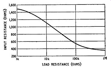
Fig. 4.2. Variation of input resistance with load resistance for a common-emitter
amplifier The vanat1on of input resistance with output collector load for
junction transistors is illustrated in Fig. 4.2.
Output Resistance
We can obtain an expression for the output resistance of the common-emitter amplifier by eliminating i,, between equations ( 1) and (3) to obtain a relationship between Vin and ic. From (3)
we have
Substituting in (1)
This can be more conveniently written in the form
(10)
In a simple circuit containing a signal source of voltage V and an internal resistance r0 feeding a load resistance Ri the current i2 is given by
.... ( 11)
If we compare expressions ( 10) and ( 11) we obtain the following
expression for the output resistance of the common-emitter amplifier:
(12)
This expression shows that the output resistance depends on the source resistance (for a given transistor), decreasing as the source resistance is increased.
This expression can be simplified by combining the first term with the third; this gives the result...
(13)
To find an expression for the output resistance for short-circuited input terminals, let R8 approach zero in expression (13). We then have...
(14)
...if we neglect the term TeTb/rc which is small compared with the others.
To find an expression for the output resistance for open-circuited input terminals let R8 approach infinity in expression (12). We then have
To = Te + Tc (1 - alpha) and as Te is small compared with rc (1 - alpha) we can say To=rc( 1-alpha) .... (15)
Output Resistance of a Junction Transistor as Common-emitter Amplifier
We can determine the range of values of output resistance for a common-emitter junction transistor amplifier by substituting the typical practical values Te = 25 ohms, Tb = 300 ohms, Tc = 1 meg ohm and alpha = 0.98 in expression (14) and (15). From (14) the output resistance for short-circuited input terminals is given by:
Te + Tb (1 - o:) To = Tc . ----- Te+ Tb
= 1000000 . 25 + 300 (I - 0·98) ohms
' ' 25 + 300 25 + 6
= 1,000,000 . ~ ohms 31
= 1,000,000. - ohms 325
=95 k-O
From expression (15) the output resistance for open-circuited input terminals is given by:
To = Tc (I - o:)
= 1,000,000 (1 - 0·98) ohms
= 1,000,000 X 0·02 ohms
=20k-ohm
The variation in output resistance with source resistance for junction transistors is illustrated in Fig. 4.3.
Voltage Gain From
Fig. 4.1 (b) we can see that the output voltage is given by icRz.
The voltage gain Vout/Vin is thus given by icRz/Vin. From ( 10) ic is given by
Hence
…
.... (16)
Normally alpha_r_c greatly exceeds re and this expression therefore gives a positive value for the voltage gain. But, to agree with the physics of the transistor, the collector current in Fig. 4.1 (b) was assumed to be flowing in an anticlockwise direction whereas the base current was shown flowing in a clockwise direction. A positive value for the voltage gain thus implies that the output voltage is inverted with respect to the input voltage. In this respect the common-emitter amplifier is similar to a common-cathode thermionic valve amplifier. Expression (16) can be simplified by neglecting Te in comparison with alpha_r_c in numerator and denominator.
SOURCE RESISTANCE (OHMS)
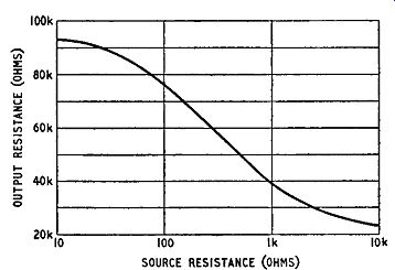
Fig. 4.3. Variation of output resistance with source resistance for a common-emitter
amplifier
We then have:
Vout _ alpha_r_c Ri Vin - [Rz + Tc (1 - ex)] (R, +Tb+ Te) + a.TeTc
For values of Ri and re small compared with Tc (I - ex) expression (16) may be written V out
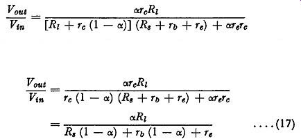
... (17)
As a numerical example suppose:
alpha = 0.98, Ri = 10 k-O, R, = 1 k-O, Te= 25 ohms and Tb= 300 ohms. We have:
Vout 0.98 X 10^4
Vin = 1,000 (1 – 0.98) + 300 (1- 0.98) + 25
0,98 X 10^4
20 + 6 + 25
0,98 X 10^4
51
= 192 more than 19 times that available from the same transistor, the same source resistance and the same load resistance in a common base amplifying circuit. However, expression (17) is similar to that for the common-base amplifier (expression 16 of Chapter 3) but contains R8 (1 -a) compared with Ra in the earlier formula. Moreover, if Ra is very small or-and this amounts to the same thing--if Vin is taken as the voltage between the input terminals of the amplifier, the two expressions for the voltage gain become equal.
Consider now the voltage gain of the common-emitter amplifier for load resistor values which are very large compared with re (1 - a). Ifre is neglected in comparison with re, expression (16) ...
... becomes Vout aTcRi Vin - Rz (Ra + Tb + re) + arero The second term in the denominator can be neglected in comparison with the others, giving V out arc Vin - Ra + Tb + Te
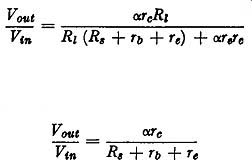
.... (18)
which is identical with expression (17) for the common-base amplifier. Thus for small source resistances or large values of load resistance the voltage gain of a given transistor with a given value of collector load resistance is approximately the same, no matter whether the transistor is connected up as a common base or a common-emitter amplifier. The curve relating voltage gain with load resistance is similar to that for the common-base amplifier and is given in Fig. 4.4.
Expression ( 16) may also be written alpha_r_c - re R
. l Vout _ Ri +re+ re (I - ex)
Vin - R + + + Te (alpha_r_c - re)
s Tb re R1 + re + re (I - ex)
Simplifying the numerator by omitting the negligible term re and substituting for r, from expression (6) we have
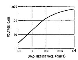
Fig. 4.4. Variation of voltage gain with load resistance for a common emitter
amplifier
If R1 is small compared with re (1 - ex) and R8 is small compared with r1 this becomes
Vout Vin
This is usually written where
-------
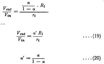
.... (19)
.... (20)
Expression ( 19) is of the type used in Chapter 2 in the simplified calculation of stage gains of transistors and it suggests that the current gain of the common-emitter circuit is equal to ex/(1 - ex). This can be confirmed from equation (3)
. re - alpha_r_c . Zc = - ----------:--- . t1> Ri + re + (1 - ex) re which on simplification and for small collector load values gives the result:
In this book the current gain of the common-emitter amplifier is represented by ex' but in some publications it is represented by /3.
Current Gain of Common-emitter Circuit
Values of exare commonly near unity and the current gain of the common-emitter circuit can be considerable. For example, if ex= 0.98 we have:
The common-emitter amplifier has an input resistance many times that of the common-base amplifier. For a given voltage across the input terminals, therefore, it takes a smaller input current.
The current gain of the common-emitter amplifier is, however, many times that of the common-base amplifier (which is always less than unity) and it is therefore not surprising that there is negligible difference between their voltage gains when the source resistance is low. If the source resistance is high, the input current has a tendency to be independent of the input resistance and is the same for both common-base and common-emitter amplifiers. The voltage gain of the common-emitter amplifier is now greater than that of the common-base amplifier because of its greater current gain.
Practical Circuit for a Common-emitter Amplifier
Fig. 4.5 gives the circuit diagram for a practical common-emitter amplifier. For simplicity this shows a single battery used for biasing the base and the collector relative to the emitter. There are alternative circuits employing a potential divider which also
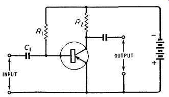
Fig. 4.5. Practical circuit for a common-emitter amplifier give protection
against thermal runaway: these are discussed more fully in Chapter 6. At
the moment we are interested in calculating suitable values for C1, R1 and
Rz. We will assume that the battery is 6 volts and that the mean collector
current is to be 1 mA. If the transistor is to be a class-A amplifier in
which the collector voltage can swing above and below its quiescent value,
a suitable quiescent voltage is - 3 volts. The voltage drop across Rz is
then 3 volts and, if the current is 1 mA, the value of Rz must be 3 kO. We
will assume alpha to be 0.98 giving alpha ' as 49. When the quiescent collector
current is 1 mA, the quiescent base current is 1/49 mA, approximately 20
µ-A. There is normally little difference between the potentials of emitter
and base, and the voltage across the base bias resistor, R1, is 6 volts.
The value of R1 is thus, from Ohm's law, 6/(20 X 10^-6), i.e. 300 k-O. The
value of C1 depends on the input resistance of the transistor and the lowest
frequency of operation. As shown earlier, the input resistance depends on
the load resistance, but may be taken as approximately 1 k-ohm. If we make
the reactance of C1 equal to 1 k-O at the lowest frequency, there will be
a 3 dB loss at this frequency. For an audio-frequency amplifier the low-frequency
limit may be 50 hz and we have = 3 µF approximately
Collector Current - Collector Voltage Characteristics for Common emitter Operation
The behavior of a common-emitter circuit such as that illustrated in Fig. 4.5 can be deduced from a set of collector current - collector
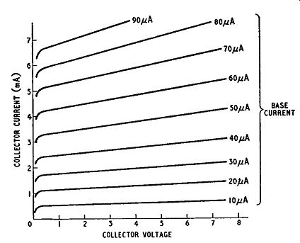
Fig. 4.6. Typical collector current-collector voltage characteristics for
common-emitter connection
voltage characteristics plotted for various values of base current.
Such a set of curves is given in Fig. 4.6. They are similar in shape to the anode current - anode voltage curves for a pentode valve but the knee of the characteristics occurs at a very low collector voltage, permitting large swings in collector voltage during amplification.
A number of parameters of the transistor can be obtained from these characteristics. For example the slope of the characteristics for collector voltages exceeding that of the knee is not as low as that for the common-base connection, showing that the effective collector a.c. resistance is smaller than for the common-base connection.
In fact, from Fig. 4.6 the effective collector a.c. resistance is approximately 30 k-ohm.
Power Gain
We have seen that the voltage gain of a common-emitter amplifier is of the same order as that of the common-base amplifier and a typical value is 100. Unlike the common-base amplifier, however, the common-emitter type has considerable current gain, a typical value of a' being 50. Thus the power gain of a common-emitter amplifier can easily amount to 5,000 (37 dB), 17 dB more than is available from a common-base amplifier.
Comparison of Common-emitter and Common-base Amplifiers
We have now discussed the properties of common-base and common-emitter amplifiers and can assess their relative advantages and disadvantages. The common-base amplifier has a very low input resistance and a very high output resistance which make the design of inter-stage matching networks or transformers difficult.
Nevertheless this circuit is used, particularly in head amplifiers where the input resistance provides a reasonable match for micro phones or pick-ups of the moving-coil type. The input resistance of the common-emitter amplifier is higher and the output resistance is lower than that of the common-base amplifier, simplifying the design of inter-stage networks and transformers. On the other hand the thermal stability of the common-emitter circuit is inferior to that of the common-base amplifier and protective circuits are essential in common-emitter amplifiers (see Chapter 6). The greater power gain of the common-emitter circuit is usually regarded as more important than the disadvantages and this circuit is extensively employed in amplifiers and receivers.