Introduction
IN Chapter 1 we discussed semiconductors and showed that a junction between n-type and p-type materials has asymmetrical conducting properties enabling it to be used for rectification. A triode junction transistor includes two such junctions and they are arranged as shown in the theoretical diagram of Fig. 2.1.
Fig. 2.1 (a) illustrates one basic type consisting of a layer of
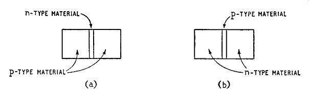
Fig. 2.1. Theoretical diagrams illustrating the structure of (a) a pnp and
(b) an npn transistor
n-type material sandwiched between two layers of p-type material: such a transistor is referred to as a pnp type.
A second type, illustrated in Fig. 2.1 (b) has a layer of p-type material sandwiched between two layers of n-type semiconducting material: such a transistor is referred to as an npn type.
In both types, for successful operation, it is essential that the central layer should be thin. However, it is not possible to construct junction transistors by placing suitably-treated layers of semi-conducting material in contact. One method which is employed is to start with a single crystal of, say, n-type germanium and to treat it so as to produce regions of p-type conductivity on either side of the remaining region of n-type conductivity.
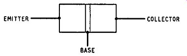
Fig. 2.2. Electrical connections to a junction transistor.
Electrical connections are made to each of the three different regions of a triode transistor as suggested in Fig. 2.2. The thin central layer is known as the base of the transistor and corresponds with the control grid of a triode valve. One of the remaining two layers is known as the emitter and corresponds with the cathode of a triode valve. For efficient operation the emitter must have much greater conductivity than the base and must of course be of the opposite conductivity, i.e. must be p-type if the base is n-type. The remaining (third) layer is known as the collector: it corresponds with the anode of the triode. The transistor may be symmetrical and either of the outer layers may then be used as emitter: the operating conditions determine which of the outer layers behaves as emitter, because in normal operation the emitter-base junction is forward biased whilst the base-collector junction is reverse-biased. In practice most junction transistors are unsymmetrical with the collector junction larger than the emitter junction and it is essential to adhere to the emitter and collector connections prescribed by the manufacturer.
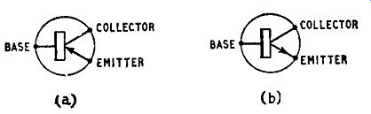
Fig. 2.3. Circuit diagram symbols for (a) a pnp and ( b) an npn junction
transistor.
The symbols used for junction transistors in circuit diagrams are given in Fig. 2.3. The symbol shown at (a), in which the emitter arrow is directed towards the base, is used for a pnp transistor and the symbol shown at (b), in which the emitter arrow is directed away from the base, is used for an npn transistor.
Construction of an alloy junction transistor
A practical form of construction for a pnp junction transistor is illustrated in Fig. 2.4. The basic element is a crystal or wafer of n-type germanium about 0.1 in. square and 0.005 in. thick. A small pellet of a trivalent element such as indium is placed near the center of each of the two opposite faces of the wafer and the combination is heated in an oven to a temperature between the melting point of indium and that of germanium. This causes the indium pellets to alloy with the germanium to form regions of p-type conductivity separated from each other by a thin layer having the n-type conductivity of the original crystal. Connecting leads are soldered to each of the indium pellets and to the germanium crystal and the assembly is hermetically sealed in a light-proof container.
For best performance from the transistor the indium pellet used as the collector electrode must usually be larger than the other. In a symmetrical transistor the indium pellets are of the same size;
METAL RING TO WHICH GERMANIUM CRYSTAL IS SOLDERED
EMITTER CONNECTION BASE CONNECTION CRYSTAL OF T1·TYPE GERMANIUM COLLECTOR CONNECTION p-TYPE GERMANIUM (DUE TO ALLOYING OF INDIUM)
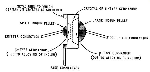
Fig. 2.4. Construction of alloy junction pnp germanium transistor this produces
a transistor more suitable for switching applications than for amplification.
A similar technique can be used to prepare npn transistors: a crystal of p-type germanium is used and pellets of a pentavalent element such as arsenic or antimony, carried perhaps in a neutral (Group IV) element such as lead, are alloyed to it. This alloying process is only one of a number of methods which can be used in the manufacture of transistors.
Operation of a pnp Transistor
Fig. 2.5 illustrates the polarity of the potentials which are necessary in a pop-transistor amplifying circuit. The emitter is biased slightly positively with respect to the base: this is an example of forward bias and the external battery opposes the internal potential barrier associated with the emitter-base junction. A considerable ...
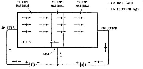
Fig. 2.5. Hole and electron paths in a pnp junction transistor connected
for amplification.
... current therefore flows across this junction and this is carried by holes from the p-type emitter (which move to the right into the base) and by electrons from the n-type base (which move to the left into the emitter). However because the impurity concentration in the emitter is normally considerably greater than that of the base (this is adjusted during manufacture), the holes carrying the emitter-base current greatly outnumber the electrons and we can say with little error that the current flowing across the emitter-base junction is carried by holes moving from emitter to base.
The collector is biased negatively with respect to the base: this is an example of reverse bias and the external battery aids the internal potential barrier associated with the base-collector junction.
If the emitter-base junction were also reverse-biased, no holes would be injected into the base region from the emitter and only a very small current would flow across the base-collector junction. This is the reverse current ( described in Chapter 1) : it is a saturation current independent of the collector-base voltage. However, when the emitter-base junction is forward-biased, the injected holes have a marked effect on the collector current: this is, in fact, the essence of transistor action. The holes are injected into the base, which is a particularly thin layer; most of them cross the base by diffusion and on reaching the collector-base junction are swept into the collector region. The reverse bias of the base-collector junction ensures the collection of all the holes crossing this junction, whether these are present in the base region as a result of breakdown of covalent bonds by virtue of thermal agitation or are injected into it by the action of the emitter. A few of the holes which leave the emitter combine with electrons in the base and so cease to exist but the majority of the holes (commonly more than 95 percent) succeed in reaching the collector. Thus the increase in collector current due to hole-injection by the emitter is nearly equal to the current flowing across the emitter-base junction. The balance of the emitter carriers (equal to, say, 5 percent) are neutralized by electrons in the base region and to maintain charge neutrality more electrons flow into the base, constituting a base current. The collector current, even though it may be considerably increased by forward bias of the emitter-base junction, is still independent of the collector voltage. This is another way of saying that the output resistance of the transistor is extremely high: it can in fact be several megohms. The input resistance is approximately that of a forward-biased junction diode and is commonly of the order of 25 ohms. A small change in the input (emitter) current of the transistor is faithfully reproduced in the output (collector) current even though the output resistance may be 40,000
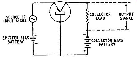
Fig. 2.6. Basic circuit for using a pnp junction transistor as an amplifier
... times the input resistance: this marked disparity between input and output resistance enables the transistor to act as a very effective power amplifier. This point is illustrated by numerical examples later in this chapter.
Bias Supplies for a pnp Transistor
Fig. 2.6 shows a pnp transistor connected to supplies as required in one form of amplifying circuit. For forward bias of the emitter base junction, the emitter is made positive with respect to the base; for reverse bias of the base-collector junction, the collector is made negative with respect to the base. Fig. 2.6 shows separate batteries used to provide these two bias supplies and it is significant that the
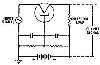
Fig. 2.7. The circuit of Fig. 2.6 using a single battery and a potential
divider providing base bias
... batteries are connected in series, the positive terminal of one being connected to the negative terminal of the other. Thus a single battery can be used to provide the two bias supplies by connecting it between emitter and collector, the base being returned to a tapping point on the battery or to a potential divider connected across the battery. The potential divider technique (illustrated in Fig. 2.7) is frequently used in transistor circuits and a pnp transistor operating with the emitter circuit earthed requires a negative collector voltage.
Operation of an npn Transistor
The action of an npn junction transistor is similar to that of a pnp type and is illustrated in Fig. 2.8 but the current carriers are largely electrons instead of holes. The emitter-base junction must be forward biased and in an npn transistor this requires the emitter to be biased negatively with respect to the base. This bias causes a considerable current to flow across the emitter-base junction, a current carried by the free electrons of the emitter and the holes of the base. The electrons are required to outnumber the holes and thus, as in a pnp transistor, the emitter region must have greater conductivity than the base region: this is ensured during manufacture. The base-collector junction is reverse-biased: in an npn transistor this requires the collector to be biased positively with respect to the base. Electrons entering the very thin base region from the emitter cross the base region by diffusion and on reaching the base-collector junction are swept into the collector region to give a collector current which is commonly about 95 percent of the emitter current.
Thus the behavior of an npn transistor is very similar to that of a pnp type with the bias polarities and directions of current flow reversed: in particular the collector supply for an npn transistor with the emitter circuit earthed must be positive.
High-frequency Performance of a Transistor
In the alloy transistor described above there is a uniform impurity concentration throughout the base region and the only changes in impurity which occur in the device do so very abruptly in the junctions separating the base from the emitter and from the collector.
As a result of the uniform impurity concentration, the base region is field-free and the current carriers (holes in a pnp transistor and electrons in an npn type) cross this region to enter the collector region only by diffusion. Diffusion is a slow process and there is a
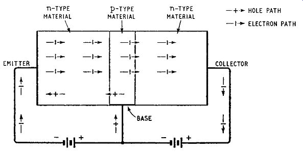
Fig. 2.8. Electron and hole paths in an npn junction transistor connected
far amplification.
... significant time delay between the application of an input signal to the emitter and the receipt of the corresponding output signal from the collector. The effect of this on the transistor performance is discussed more fully later in this chapter but it is similar to the effect of electron transit time on the performance of a thermionic valve: that is to say it degrades the performance of the transistor as signal frequency is increased and in fact sets an upper limit to the frequency at which the transistor can be used satisfactorily. To obtain a good performance at high frequencies the time taken by the current carriers to cross the base must be reduced to a minimum.
One method commonly employed to reduce transit time in a transistor is to reduce the thickness of the base region but this may limit the maximum permitted collector voltage to a few volts.
However, it is scarcely practicable to raise the uppermost working frequency of a uniform-base transistor much above 20 Mhz by this method alone.
Drift Transistor
Another method of reducing transit time in a transistor is to vary the impurity concentration through the base region so as to produce an electric field which aids the passage of current carriers across the base region. To give this effect, the impurity concentration must be a maximum near the emitter junction and a minimum near the collector junction and an exponential distribution is a suitable one to use.
Transistors with such a base region are known as drift transistors (because the motion of the current carriers from emitter to collector is mainly a drift imposed by the field in the base region) and have a much reduced transit time, giving a high-frequency performance much superior to that of a uniform-base type.
The technique of solid-state diffusion may be employed to produce the graded base region for drift transistors. One method is to expose the semiconductor material to a vapor of the desired impurity in a furnace. This causes impurity atoms to diffuse into the crystal structure to give an impurity concentration which falls off as the depth of penetration increases. By this means it is possible to produce a base region of accurately-controlled thickness and of graded impurity content. Drift transistors can be made using wafers of such material by alloying pellets to the two faces of the wafer as described at the beginning of this chapter. Theoretically the uppermost working frequency of a transistor can be improved by up to 8 times by grading the impurity concentration in the base region, and in practice, drift transistors of this type operate satisfactorily up to 50 Mhz. With special care and attention in manufacture such transistors can be used at frequencies up to 150 Mhz, making possible the construction of fully-transistorized v.h.f. equipment such as f.m. receivers.
Mesa Transistor
A form of construction often adopted for drift transistors is the so-called Mesa form illustrated in Fig. 2.9. This has the advantage of giving low collector-base capacitance and good collector dissipation. The collector region is a block of, say, p-type semiconductor material large enough to permit collector dissipation up to 0.5W,
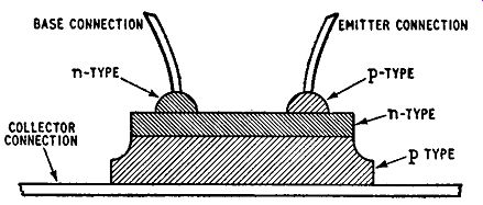
Fig. 2.9. Construction of a Mesa transistor
even at frequencies of hundreds of Mhz. An n-type base region is formed on the upper surface of this block by diffusion and two pellets of semiconductor material are alloyed to the n-region; one pellet is of n-type material to form the base connection and the other is of p-type material to form the emitter connection. Mesa transistors of this type have operated satisfactorily at frequencies up to 1,000 Mhz.
CURRENT AMPLIFICATION FACTOR
The ratio of a small change in collector current ic to the small change in emitter current ie which gives rise to it is known as the current amplification factor and is represented by ex. It is measured with a short-circuited output. Thus we have for a junction transistor excannot exceed unity and is usually between 0.95 and 0.99 corresponding to the 95% or greater capture of emitter current by the collector mentioned on p. 23.
The current amplification factor for a transistor can be compared with the voltage amplification factor µ, for a thermionic valve, which can be defined as the ratio of the voltage acting in the anode circuit to the voltage applied to the grid which gives rise to it.
It is characteristic of a valve that the voltage in the output circuit is directly related to the input voltage: for this reason valves are referred to as voltage-operated devices. Similarly it is characteristic of transistors that the current flowing in the output circuit is directly related to the input current: for this reason transistors are referred to as current-operated devices. This does not mean, of course, that transistors cannot be used as voltage amplifiers: they are, in fact, often so used and in the next section we shall calculate the voltage gain obtainable from transistor voltage amplifiers.
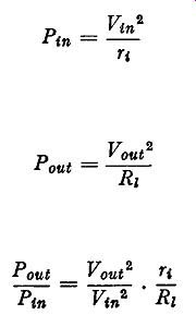
VOLTAGE GAIN OF A TRANSISTOR AMPLIFIER
The voltage gain obtainable from a number of commonly-employed transistor circuits is calculated in detail in Chapters 3 to 5. However, some simple introductory calculations are given at this point.
These apply to the simple circuit of Fig. 2.7: this is an example of the common-base type of amplifier described in Chapter 3. We know from the fundamental nature of transistors that the alternating component of the collector current is extimes the alternating component of the emitter current. As a current amplifier, therefore, the gain has an upper limiting value of l for a junction transistor.
An approximate estimate of the voltage gain can be obtained by assuming the current gain to be unity, that is, by assuming that the alternating components of the emitter and collector currents are equal. In effect, therefore, the signal current passes straight through the transistor without significant change in value. Thus a signal voltage applied to the low-value input resistance gives an input current (readily calculated from Ohm's law) which appears at the output terminals as though it had originated from a high resistance source. The high-resistance source is important for it means that high-value load resistors may be used without significantly affecting the output current: in this way high voltage gains may be achieved.
For example suppose the input resistance is 50 ohms and the load resistance 4.7 k-O. An input voltage of l mV gives rise to an input current ie where:
=20µ.A
If the current amplification factor is taken as unity this is also the collector current ic, The output voltage Vout is given by the product of output current and load resistance.
Vout = icRz
= 20 X 10^-6 X 4,700 volts
=94mV
The voltage gain is thus 94, equal to the ratio of the load resistance to the input resistance.
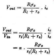
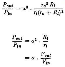
A more accurate though still simple calculation of the voltage gain of a transistor amplifier can be performed as follows. The relationship between input voltage Vin and emitter current i_e is given by Vin= ier, where Tf = input resistance of the transistor.
The relationship between output voltage V out and collector current is a little more complicated because the effective resistance of this circuit is composed of the output resistance and the collector load resistance in parallel. Thus we have
V out = Rir o . Zc Ri + To
The voltage gain of the amplifier is thus given by
Vout _ R1ro ic Vin - T1(R1 + To) . ie R1To
=at.--- T1(R1 + To)
Usually transistor amplifiers are operated from low-voltage supplies such as 6 or 12 volts and the collector current (steady component) is often of the order of 1 mA.
Thus the collector load resistance cannot exceed a few thousands of ohms and is commonly 4.7 k-ohm.
This is small compared with To for junction transistors and thus the above expression for the voltage gain can be simplified to
Vout Rz
-=<X, Vin Tf
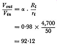
showing the gain to be directly proportional to the current amplification factor and the collector load resistance but inversely proportional to the input resistance. As a numerical example, suppose a junction transistor has ex= 0.98, r, = 50-ohms and R,, =4.7 k-ohm.
The voltage gain is given by Vout Ri
--=ex. Vin r,
= 0.98 X 4,700 50
= 92x12
These calculations were made on the assumption that the effective collector load resistance is 4.7 k-ohm. If a number of transistors are connected in cascade as in a multi-stage amplifier, even though the collector circuits may include a 4.7 k-ohm resistor, the effective load resistance for any one transistor must be less than the input resistance of the following transistor. The stage gain for such a load value is limited to alpha as shown by putting R_l equal to r_i in the above expression for the voltage gain.
It is, however, possible to obtain voltage gains much higher than this in cascaded amplifiers and some of the circuits which can be used for this purpose are described in Chapters 3 to 5.
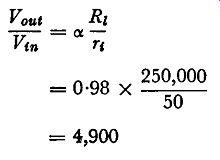
Provided the load resistance for a transistor is small compared with the output resistance, the voltage gain is proportional to the load resistance. Thus very high voltage gains can be obtained by using high-value collector load resistances: such loads, however, necessitate high values of h.t. supply and moreover should not be shunted by any circuit which reduces the effective load resistance unduly.
Such conditions exist in a valve amplifier which uses a transistor as a pre-amplifying stage. If the amplifier has a 250 volt supply the transistor can have a collector load of 250 k-ohm which allows a collector current of nearly 1 mA. If ex= 0.98 and r, = 50 ohms the voltage gain available is given by:
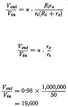
This is a surprisingly large gain, which prompts enquiry into the theoretical maximum. This can easily be calculated from the general expression
This expression approaches a maximum value as Rz approaches infinity and the maximum is given by
If ex= 0.98, r0 = 1 megohm and r, = 50 ohms, the maximum voltage gain is given by Vout = 0·98 X Vin
= 19,600 1,000,000 50
Thus the theoretical maximum voltage gain from a junction transistor is very high indeed but it is largely of theoretical interest because it is possible to realize only a small fraction of it with low values of collector supply voltage.
POWER GAIN OF A TRANSISTOR
The signal input power applied to a transistor amplifier is given by
The power delivered by the transistor to the external collector load resistance is given by:
Vout 2 Pout= - Rz
The power gain of the amplifier is thus given by
Substituting for V 01Jt/Vin from the general expression for the voltage gain given above we have, for the common-base amplifier
Potit 2 ro2 Rz
-- = ex. ---- P,11 r,(r0 + Rz) 2
If, as is usually true in practice, Rz is small compared with r 0 , this simplifies to Pout 2 Rz
-- =a . -
P,11 r, Vout
=a.- V_in a result which could have been deduced more simply from first principles. For if the voltage gain of an amplifier is given by V0ue/Vin and if the current gain is given by a, the power gain must be the product of these two, namely a Vout/Vin-
This more rigorous deduction was, however, deliberately introduced because it reminds us of an essential qualification of this result, namely that it applies only when the collector load resistance is small compared with the amplifier output resistance. For such small loads, the power gain is a times the voltage gain. For a junction transistor the power gain is slightly less than the voltage gain and, to a first degree of approximation, may be taken as equal to it.
VARIATION OF CURRENT AMPLIFICATION FACTOR WITH FREQUENCY
It was pointed out in the earlier part of this chapter that electrons and holes subjected to electric fields move with a finite velocity in semiconductors. They therefore take an appreciable time to travel between the emitter and collector of a junction transistor and there is a significant time delay between the application of an input signal to the emitter and the receipt of the corresponding output signal from the collector. If this time were constant for all electrons or all holes travelling through the transistor, the output signal would be delayed but not distorted and the effect of the finite velocity of the current carriers would be unimportant in many applications. Unfortunately all the current carriers do not have the same velocity: there is an average velocity and most of the current carriers have a velocity which does not greatly differ from this average value. A small number of current carriers, however, have velocities markedly lower or higher than the average value.
The distribution of velocities, in fact, follows the curve illustrated in Fig. 2.10 which is well known to statisticians as indicating so-called Gaussian distribution. The horizontal axis gives electron ( or hole) velocities, and the ordinate at any particular value of
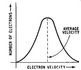
Fig. 2.10. Distributing of electron velocities about the average value
velocity indicates the likelihood of an electron ( or hole) having that velocity. The curve naturally shows a maximum at the average value of velocity.
The variation in velocity about the mean value is analogous to dispersion and it causes distortion of the output signal. The precise form of the distortion is best illustrated by considering the amplification of a steep-sided signal such as the leading edge of a rectangular pulse illustrated in Fig. 2.11. Such a signal is usually
Fig. 2.11. A step signal TIME referred to as a step signal and its most
important property is the very small time it takes to rise to its maximum
value. This is measured by the rise time of the step signal, defined as the
time taken for the voltage to rise from 10 percent to 90 percent of the final
steady value. When a step signal is applied to the emitter circuit of a junction
transistor it starts a flow of electrons (or holes) to the collector. The
most rapid of the current carriers arrive at the collector very quickly,
the majority arrive a little later, and the slowest arrive later still. Thus
the output signal has the form shown in Fig. 2.12. The most significant feature
of this waveform, apart from the fact that it is delayed with respect to
the input
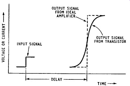
Fig. 2.12. Form of distortion due to variation in current-carrier velocity
in a junction transistor
... signal, is that it is not so steep as the input signal: in other words, the rise time has been increased by amplification in the transistor.
Fourier analysis of a single step signal shows that it has a continuous spectrum extending from zero frequency to an upper limit which depends on the steepness of the step. The steeper the step the more extended is the high-frequency response. In fact there is a simple but approximate relationship between the rise time of a step signal and the upper frequency limit of its spectrum. The relationship is f max = 2 X rise time
Thus an increase in rise time, such as occurs as a result of variation in current-carrier velocity, means that the output signal does not have such an extensive high-frequency response content as the input signal. A high-frequency loss has occurred in the transistor: the current amplification factor falls as frequency increases.
Although variation in current-carrier velocity is one of the chief causes of high-frequency loss in a junction transistor, it is certainly not the only one. Losses also occur as a result of the internal capacitance in the transistor which inevitably shunts the collector and emitter circuits. Further information on losses due to this source is given in Chapter 8.
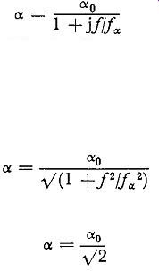
ALPHA CUT-OFF FREQUENCY
For an alloy junction transistor with a uniform base region the rate of fall of current amplification factor (and the associated phase shift) are approximately expressed by the equation alpha
alpha = 1 + jfffx
where alpha = current amplification factor at a frequency f
alpha = current amplification factor at low frequencies
and fa. = a frequency characteristic of the transistor.
From this expression the numerical value of the current amplification factor is given by and at the frequency fa. the numerical value is given by i.e. fa. is the frequency at which the current amplification factor has fallen to 1/__/2 i.e. 0.707 of the low-frequency value: this corresponds to a loss of 3 dB. The alpha cut-off frequency is thus defined as the frequency at which the current amplification factor of the common-base amplifier (with short-circuited output) has fallen by 3 dB. The value of the alpha cut-off frequency depends on the area of the emitter and collector junctions and on the thickness of the base region: in practice values for uniform-base alloy junction transistors lie between 10 khz for transistors intended for outputs of several watts to 20 Mhz for transistors intended for r.f. applications.
FREQUENCY f1
The expressions given in the above section represent the gain and phase shift in uniform-base alloy junction transistors with reasonable accuracy, but considerable errors can occur if the expressions are used for transistors containing a drift field in the base region. For such transistors it is better to express the high-frequency performance in terms of another frequency parameter f 1 which is defined as the frequency at which the real part of the current amplification factor has fallen to one half the low-frequency value.
For a non-drift transistor the current amplification factor has a value of alpha_0/ __/2 at fa. and the phase angle is 45°: the real part of exis thus equal to (alpha_ 0 cos 45) / __/2, i.e. alpha_ 0/2. For such a transistor, therefore, fa. and f 1 are equal but for drift transistors, fa. can be as much as twice f 1 depending on the magnitude of the drift field.
The frequency f 1 gives a more useful indication of high-frequency performance than fa. For example, f 1 is approximately equal to the frequency at which the current gain of a common-emitter amplifier (with short-circuited output) has fallen to unity. It thus measures the highest frequency at which the transistor can be used as an amplifier. It also measures the gain-bandwidth product of the transistor when used as a common-emitter amplifier.